EP0222396A1 - Dispositif de transistors à effet de champ - Google Patents
Dispositif de transistors à effet de champ Download PDFInfo
- Publication number
- EP0222396A1 EP0222396A1 EP86115726A EP86115726A EP0222396A1 EP 0222396 A1 EP0222396 A1 EP 0222396A1 EP 86115726 A EP86115726 A EP 86115726A EP 86115726 A EP86115726 A EP 86115726A EP 0222396 A1 EP0222396 A1 EP 0222396A1
- Authority
- EP
- European Patent Office
- Prior art keywords
- field
- transistors
- transistor device
- effect transistor
- effect
- Prior art date
- Legal status (The legal status is an assumption and is not a legal conclusion. Google has not performed a legal analysis and makes no representation as to the accuracy of the status listed.)
- Granted
Links
Images


Classifications
-
- G—PHYSICS
- G11—INFORMATION STORAGE
- G11C—STATIC STORES
- G11C11/00—Digital stores characterised by the use of particular electric or magnetic storage elements; Storage elements therefor
- G11C11/21—Digital stores characterised by the use of particular electric or magnetic storage elements; Storage elements therefor using electric elements
- G11C11/34—Digital stores characterised by the use of particular electric or magnetic storage elements; Storage elements therefor using electric elements using semiconductor devices
- G11C11/40—Digital stores characterised by the use of particular electric or magnetic storage elements; Storage elements therefor using electric elements using semiconductor devices using transistors
- G11C11/401—Digital stores characterised by the use of particular electric or magnetic storage elements; Storage elements therefor using electric elements using semiconductor devices using transistors forming cells needing refreshing or charge regeneration, i.e. dynamic cells
- G11C11/4063—Auxiliary circuits, e.g. for addressing, decoding, driving, writing, sensing or timing
- G11C11/407—Auxiliary circuits, e.g. for addressing, decoding, driving, writing, sensing or timing for memory cells of the field-effect type
- G11C11/409—Read-write [R-W] circuits
- G11C11/4091—Sense or sense/refresh amplifiers, or associated sense circuitry, e.g. for coupled bit-line precharging, equalising or isolating
-
- G—PHYSICS
- G11—INFORMATION STORAGE
- G11C—STATIC STORES
- G11C11/00—Digital stores characterised by the use of particular electric or magnetic storage elements; Storage elements therefor
- G11C11/21—Digital stores characterised by the use of particular electric or magnetic storage elements; Storage elements therefor using electric elements
- G11C11/34—Digital stores characterised by the use of particular electric or magnetic storage elements; Storage elements therefor using electric elements using semiconductor devices
- G11C11/40—Digital stores characterised by the use of particular electric or magnetic storage elements; Storage elements therefor using electric elements using semiconductor devices using transistors
- G11C11/41—Digital stores characterised by the use of particular electric or magnetic storage elements; Storage elements therefor using electric elements using semiconductor devices using transistors forming static cells with positive feedback, i.e. cells not needing refreshing or charge regeneration, e.g. bistable multivibrator or Schmitt trigger
- G11C11/412—Digital stores characterised by the use of particular electric or magnetic storage elements; Storage elements therefor using electric elements using semiconductor devices using transistors forming static cells with positive feedback, i.e. cells not needing refreshing or charge regeneration, e.g. bistable multivibrator or Schmitt trigger using field-effect transistors only
-
- H—ELECTRICITY
- H10—SEMICONDUCTOR DEVICES; ELECTRIC SOLID-STATE DEVICES NOT OTHERWISE PROVIDED FOR
- H10B—ELECTRONIC MEMORY DEVICES
- H10B12/00—Dynamic random access memory [DRAM] devices
-
- H—ELECTRICITY
- H10—SEMICONDUCTOR DEVICES; ELECTRIC SOLID-STATE DEVICES NOT OTHERWISE PROVIDED FOR
- H10D—INORGANIC ELECTRIC SEMICONDUCTOR DEVICES
- H10D84/00—Integrated devices formed in or on semiconductor substrates that comprise only semiconducting layers, e.g. on Si wafers or on GaAs-on-Si wafers
- H10D84/80—Integrated devices formed in or on semiconductor substrates that comprise only semiconducting layers, e.g. on Si wafers or on GaAs-on-Si wafers characterised by the integration of at least one component covered by groups H10D12/00 or H10D30/00, e.g. integration of IGFETs
- H10D84/82—Integrated devices formed in or on semiconductor substrates that comprise only semiconducting layers, e.g. on Si wafers or on GaAs-on-Si wafers characterised by the integration of at least one component covered by groups H10D12/00 or H10D30/00, e.g. integration of IGFETs of only field-effect components
- H10D84/83—Integrated devices formed in or on semiconductor substrates that comprise only semiconducting layers, e.g. on Si wafers or on GaAs-on-Si wafers characterised by the integration of at least one component covered by groups H10D12/00 or H10D30/00, e.g. integration of IGFETs of only field-effect components of only insulated-gate FETs [IGFET]
- H10D84/85—Complementary IGFETs, e.g. CMOS
-
- Y—GENERAL TAGGING OF NEW TECHNOLOGICAL DEVELOPMENTS; GENERAL TAGGING OF CROSS-SECTIONAL TECHNOLOGIES SPANNING OVER SEVERAL SECTIONS OF THE IPC; TECHNICAL SUBJECTS COVERED BY FORMER USPC CROSS-REFERENCE ART COLLECTIONS [XRACs] AND DIGESTS
- Y10—TECHNICAL SUBJECTS COVERED BY FORMER USPC
- Y10S—TECHNICAL SUBJECTS COVERED BY FORMER USPC CROSS-REFERENCE ART COLLECTIONS [XRACs] AND DIGESTS
- Y10S257/00—Active solid-state devices, e.g. transistors, solid-state diodes
- Y10S257/919—Elements of similar construction connected in series or parallel to average out manufacturing variations in characteristics
Definitions
- the present invention relates to a field-effect transistor device, and more particularly to a field-effect transistor device having a plurality of MIS transistors forming a sense amplifier.
- Fig. 1 shows a latch-type sense amplifier having N-channel MOS transistors Ql and Q2.
- Bit lines BL and BL are set at the same potential before data is transferred through them. Their potential varies when the data is transferred through them.
- Enable signal SAE is at the V DD level, e.g., 5 V. It falls to the V SS level, e.g., 0 V, in order to sense a potential difference corresponding to the data supplied to bit lines BL and BL.
- V SS level e.g., 0 V
- MOS transistors Ql and Q2 are activated, thereby amplifying the potential difference to a predetermined level. More specifically, the sense amplifier sets one of the bit lines BL and BL at the V DD level, and sets the other bit line at the V SS level.
- Fig. 2 is a plan view of the sense amplifier shown in Fig. 1, which is formed on a semiconductor memory chip.
- Wiring layers 10A and 10B are, for example, formed of Aluminum, electrically insulated from semiconductor substrate 12, and extend in the same direction.
- Gate electrode 14A of MOS transistor Q2 and gate electrode 14B of MOS transistor Ql are also insulated from substrate 12, and extend in the same direction as wiring layers l0A and 10B.
- Gate electrodes 14A and 14B are made, for example, of polycrystalline silicon. Both end portions of gate electrode 14A are overlapped by aluminum layers 10A. Similarly, both end portions of gate electrode 14B are overlapped by wiring layers 10B.
- Aluminum wiring layers 10A are connected to the ends of gate electrode 14A by means of contact holes 16A, thereby forming bit line BL.
- Aluminum wiring layers 10B are coupled to the ends of gate electrode 14B by means of contact holes 16B, thereby forming bit line BL.
- Drain region 18A and source region 18B of MOS transistor Ql are formed within substrate 12, on the left and right sides of gate electrode 14B, respectively.
- Source region 20A and drain region 20B of MOS transistor Q2 are formed within substrate 12, on the left and right sides of gate electrode 14A, respectively.
- One of wiring layers 10A is connected to drain region 18A by means of contact hole 22A, and one of wiring layers 10B is connected to drain region 20B by means of contact hole 22B.
- Conductor layers 24A and 24B are formed in contact with source regions 18B and 20A.
- a wiring layer 26 is connected to conductor layer 24A by means of contact hole 28A and to conductor layer 24B by means of contact hole 28B.
- Wiring layers 10A, 10B and 26 and gate electrodes 14A and 14B are electrically insulated from one another by insulation layers (not shown).
- Source region 18B and 20A and drain regions 18A and 20B have been simultaneously formed and self-aligned by ion-implantation of impurities, using gate electrodes 14A and 14B as masks. Ion implantation of this type is usually performed, as is illustrated in Fig. 3, in order to suppress the channeling effect. More specifically, the impurity ions are implanted into substrate 10 in the direction inclined to the surface of substrate 10 at a predetermined angle. Gate electrode 30 traps the impurity ions moving toward portion 31 of substrate 10. As a result, the implanted impurity ions are distributed in the substrate 10 asymmetrically with respect to the gate electrode 30.
- drain and source regions 18A and 18B of transistor Ql are located on the right and left sides of gate electrode 14B, respectively, and, in contrast, drain and source regions 20B and 20A of transistor Q2 are positioned on the left and right sides of gate electrode 14A, respectively.
- transistors Ql and Q2 inevitably have different characteristics. This difference is prominent, particularly when transistors Ql and Q2 have a lightly-doped drain structure.
- the driving ability (or, drain current) of transistor Ql differs from that of transistor Q2 by about 30 % at most.
- the sensitivity of the sense amplifier falls below the design value. If the sense amplifier is to function as desired, a greater potential difference must be provided between bit lines BL and BL. Also due to the difference in driving ability, the time required for providing a sufficient potential difference between bit lines BL and BL can become longer than the maximum tolerance value. This time depends on the sensed difference in potential, i.e., the data being transferred through bit lines BL and BL. It also depends on whether lines BL and BL are set at the V DD level and the V SS level, or vice versa. If this sense amplifier, which operates slowly, is used in a dynamic RA M whose memory cells must be refreshed frequently, it will cause the RAM to mulfunc- tion.
- Fig. 4 shows a sense amplifier of CMOS structure generally used.
- the MOS transistors forming this CMOS sense amplifier usually have different driving abilities due to the ion implantation. Hence, the operation of the CMOS sense amplifier cannot always meet the design specifications.
- a field-effect transistor device comprising a semiconductor substrate; a plurality of field-effect transistors, each having a gate electrode formed over the semiconductor substrate and source and drain regions self-aligned in the semiconductor substrate on two opposing sides of the gate electrode, respectively, the source-to-drain paths of the field-effect transistors being oriented in the same direction; and wiring means for connecting the plurality of the field- effect transistors.
- the field-effect transistors forming the field- effect transistor device can have the same characteristics for the following reasons.
- impurity ions are implanted into the semiconductor substrate in a direction inclined to the surface of the substrate at a predetermined angle
- the distribution of the impurity ions in the source and drain regions of either field-effect transistor are asymmetrical with respect to the,gate electrode.
- the field-effect transistors can have source regions with the same distribution of impurity ions and drain regions with the same distribution of impurity ions, since the source-to-drain paths of the field- effect transistors are oriented in the same direction.
- the field-effect transistor device can have a higher driving ability than the case where the source-to-drain paths of the field-effect transistors are oriented in the opposite directions.
- a first embodiment of the invention i.e., a latch-type sense amplifier unit, will be described with reference to Fig. 5 which is a plan view.
- the sense amplifier unit is combined with memory cells (not shown) to form a semiconductor memory such as a dynamic RAM.
- This sense amplifier unit comprises two sense amplifiers 50A and 50B which each are equivalent to the circuit of the sense amplifier illustrated in Fig. 1.
- Sense amplifier 50A has conductor layers 52A and 52B provided on an insulation layer (not shown) formed on p-type silicon substrate 54. Conductor layers 52A and 52B each serve as a gate electrode and a conductor. Similarly, sense amplifier 50B has conductor layers 52C and 52D provided on the insulation layer. Conductor layers 52C and 52D each serve as a gate electrode and a conductor. Conductor layers 52A to 52D are formed, for instance, of polycrystalline silicon. As shown in Fig. 5, those portions (or electrode portions) of layers 52A to 52D which function as gate electrodes extend in the same direction.
- Sense amplifiers 50A and 50B also have n-type regions 56A to 56F. Regions 56A to 56F have been formed in self alignment in substrate 54 by implanting impurity ions into substrate 54, using the electrode portion of conductor layers 52A to 52D as masks.
- conductor layers 58A to 58H are provided above semiconductor regions 56A to 56F and substrate 54, and are electrically insulated therefrom.
- Layers 58A, 58C, 58E, 58F, 58G, and 58H extend in parallel to the electrode portions of conductor layers 52A to 52D.
- Layers 58B and 58D extend parallel to conductor layers 52A to 52D except in the space between regions 56A to 56C and regions 56D to 56F.
- Layers 58A, 58B, 58C and 58D are connected to regions 56A, 56C, 56D and 56F, by means of contact holes 60A, 60B, 60C and 60D.
- Conductor layer 52A is connected at one end to conductor layer 58E by means of contact hole 62A, and at the other end to conductor layer 58B by means of contact hole 62B.
- Conductor layer 52B is coupled at one end to conductor layer 58A by means of contact hole 62C, and at the other end to conductor layer 58F by means of contact hole 62D.
- Conductor layer 52C is coupled at one end to conductor layer 58G by means of contact hole 62E, and at the other end to conductor layer 58D by means of contact hole 62F.
- Conductor layer 52D is coupled at one end to conductor layer 58C by means of contact hole 62G, and at the other end to conductor layer 58H by means of contact hole 62H.
- Electrode layers 64A and 64B are formed in contact with regions 56A and 56B, respectively.
- Conductor layer 68 is formed above substrate 54, regions 56A to 56F, conductor layers 52A to 52D and conductor layers 58A to 58H, and are electrically insulated therefrom. Layer 68 extends at right angles to the electrode portions of conductor layers 52A to 52D.
- Conductor layer 68 is made, for example, of aluminum and is connected to electrode layers 64A and 64B by means of contact holes 70A and 70B.
- conductor layer 52A and regions 56A and 56B form n-channel MOS transistor Ql
- conductor layer 52B and regions 56D and 56E form n-channel MOS transistor Q2.
- Conductor layers 58A, 52B and 58F form bit line BL.
- Conductor layers 58E, 52A and 58B form bit line BL.
- Enable signal SAE is supplied to conductor layer 68.
- Bit lines BL and BL intersect with each other in the space between MOS transistors Ql and Q2. They extend parallel in other locations. Hence, regions 56A and 56B function as the drain and source of MOS transistor Ql, and regions 56D and 56E function as the drain and source of MOS transistor Q2. Therefore, in substrate 54, the source-to-drain path of MOS transistor Ql is oriented in the same direction as the source-to-drain path of MOS transistor Q2.
- the ion implantation for forming regions 56A to 56F can be performed under the same conditions on both MOS transistors Ql and Q2. Both MOS transistors can, therefore, have the identical driving ability, and such problems that would result from a difference in the driving ability can be avoided.
- Fig. 6 is a partially sectional, plan view of a CMOS sense amplifier unit according to a second embodiment of the present invention.
- This embodiment has two CMOS sense amplifiers 72A and 72B which each are equivalent to the circuit of the CMOS sense amplifier shown in Fig. 4.
- Fig. 6 the same numerals are used to designate the same elements as used in the unit of Fig. 5, and primed numerals denote the elements not provided in the unit of Fig. 5.
- the CMOS sense amplifier comprises n-type well 74 formed in substrate 54, and p-type regions 76A to 76F formed in n-type well 74. Regions 76A to 76F are formed and self-aligned by implanting impurity ions into well 74, using those portions of conductor layers 52A' to 52D' which functions as gate electrodes.
- Enable signal SAE which is an inverse to enable signal SAE, is supplied to conductor layer 68'.
- conductor layer 52A' and regions 76A and 76B form p-channel MOS transistor Q4, and conductor layer 52B' and regions 76D and 76E form p-channel MOS transistor Q3.
- Conductor layers 58A, 52B, 58F, 58E', 52A' and 58B' form bit line BL.
- Conductor layers 58E, 52A, 58B, 58A', 52B' and 58F' form bit line BL.
- bit lines BL and BL intersect with each other in the space between n-channel MOS transistors Ql and Q2, and also in the space between p-channel MOS transistors Q3 and Q4. They extend in parallel in other locations.
- regions 56A and 56B function as the drain and source of MOS transistor Ql
- regions 56D and 56E function as the drain and source of MOS transistor Q2
- regions 76D and 76E function as the drain and source of MOS transistor Q3
- region 76A and 76B function as the drain and source of MOS transistor Q4. Therefore, in substrate 54, the source-to-drain paths of all MOS transistors Ql to Q4 are oriented in the same direction. Therefore, the second embodiment can accomplish the same advantages as the first embodiment.
- bit lines BL and BL which are made of polycrystalline silicon have different lengths. Bit lines BL and BL therefore have different capacitances.
- bit lines BL and BL therefore have different capacitances.
- those portions of bit lines BL and BL which are made of polycrystalline silicon have the same length, and bit lines BL and BL have the same capacitance.
- the CMOS sense amplifier unit of Fig. 6 is free from a decrease in sensitivity.
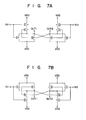
- the present invention is not limited to the above embodiments. It can be applied to CMOS flip-flops of the types illustrated in Fig. 7A and 7B.
- each gate electrode can be of the Schottky barrier type which can be formed directly on a semiconductor substrate.
Landscapes
- Engineering & Computer Science (AREA)
- Microelectronics & Electronic Packaging (AREA)
- Computer Hardware Design (AREA)
- Semiconductor Memories (AREA)
- Dram (AREA)
- Metal-Oxide And Bipolar Metal-Oxide Semiconductor Integrated Circuits (AREA)
- Amplifiers (AREA)
Applications Claiming Priority (2)
| Application Number | Priority Date | Filing Date | Title |
|---|---|---|---|
| JP256084/85 | 1985-11-15 | ||
| JP60256084A JPH0642537B2 (ja) | 1985-11-15 | 1985-11-15 | 半導体装置 |
Publications (2)
| Publication Number | Publication Date |
|---|---|
| EP0222396A1 true EP0222396A1 (fr) | 1987-05-20 |
| EP0222396B1 EP0222396B1 (fr) | 1991-01-23 |
Family
ID=17287667
Family Applications (1)
| Application Number | Title | Priority Date | Filing Date |
|---|---|---|---|
| EP86115726A Expired - Lifetime EP0222396B1 (fr) | 1985-11-15 | 1986-11-12 | Dispositif de transistors à effet de champ |
Country Status (5)
| Country | Link |
|---|---|
| US (1) | US5175604A (fr) |
| EP (1) | EP0222396B1 (fr) |
| JP (1) | JPH0642537B2 (fr) |
| KR (1) | KR910001159B1 (fr) |
| DE (1) | DE3677141D1 (fr) |
Cited By (3)
| Publication number | Priority date | Publication date | Assignee | Title |
|---|---|---|---|---|
| EP0562600A3 (en) * | 1992-03-27 | 1993-11-24 | Matsushita Electric Industrial Co Ltd | A semiconductor device having at least one symmetrical pair of mosfets |
| WO1996035234A1 (fr) * | 1995-05-01 | 1996-11-07 | Micron Technology, Inc. | Circuit peripherique d'une memoire a semi-conducteurs |
| USRE38647E1 (en) | 1987-10-02 | 2004-11-09 | Matsushita Electric Industrial Co., Ltd. | Sense amplifier circuit |
Families Citing this family (9)
| Publication number | Priority date | Publication date | Assignee | Title |
|---|---|---|---|---|
| JPH01130574A (ja) * | 1987-11-17 | 1989-05-23 | Rohm Co Ltd | 半導体装置 |
| JPH0738547B2 (ja) * | 1988-07-25 | 1995-04-26 | 日本電気株式会社 | 演算増幅器 |
| JP2700489B2 (ja) * | 1989-05-18 | 1998-01-21 | 三菱電機株式会社 | 半導体記憶装置 |
| US5289040A (en) * | 1991-08-12 | 1994-02-22 | National Semiconductor Corporation | Compensating lead structure for distributed IC components |
| JP3533227B2 (ja) * | 1992-09-10 | 2004-05-31 | 株式会社日立製作所 | 半導体記憶装置 |
| JP3004177B2 (ja) * | 1993-09-16 | 2000-01-31 | 株式会社東芝 | 半導体集積回路装置 |
| JP2004235515A (ja) | 2003-01-31 | 2004-08-19 | Renesas Technology Corp | 半導体装置 |
| US20080031029A1 (en) * | 2006-08-05 | 2008-02-07 | Taiwan Semiconductor Manufacturing Co., Ltd. | Semiconductor memory device with split bit-line structure |
| KR100761854B1 (ko) | 2006-08-08 | 2007-09-28 | 삼성전자주식회사 | 비트라인 이퀄라이저 및 이를 구비하는 반도체 메모리장치, 그리고 비트라인 이퀄라이저의 제조 방법 |
Citations (3)
| Publication number | Priority date | Publication date | Assignee | Title |
|---|---|---|---|---|
| FR2358725A1 (fr) * | 1976-07-12 | 1978-02-10 | Nippon Electric Co | Circuit de memoire a cellules a un transistor par bit |
| EP0056433A2 (fr) * | 1981-01-19 | 1982-07-28 | Siemens Aktiengesellschaft | Circuit de lecture pour une mémoire monolithique intégrée semiconductrice |
| JPS5927101B2 (ja) * | 1976-06-21 | 1984-07-03 | 日本電信電話株式会社 | 半導体装置 |
Family Cites Families (18)
| Publication number | Priority date | Publication date | Assignee | Title |
|---|---|---|---|---|
| US3477031A (en) * | 1966-09-09 | 1969-11-04 | Hitachi Ltd | Differential amplifier circuit employing multiple differential amplifier stages |
| FR1563879A (fr) * | 1968-02-09 | 1969-04-18 | ||
| JPS53675B2 (fr) * | 1972-03-16 | 1978-01-11 | ||
| JPS5925381B2 (ja) * | 1977-12-30 | 1984-06-16 | 富士通株式会社 | 半導体集積回路装置 |
| JPS55115353A (en) * | 1979-02-27 | 1980-09-05 | Fujitsu Ltd | Cell rotatable by 90 |
| JPS5615079A (en) * | 1979-07-16 | 1981-02-13 | Mitsubishi Electric Corp | Insulated gate field effect transistor couple |
| US4280855A (en) * | 1980-01-23 | 1981-07-28 | Ibm Corporation | Method of making a dual DMOS device by ion implantation and diffusion |
| US4356504A (en) * | 1980-03-28 | 1982-10-26 | International Microcircuits, Inc. | MOS Integrated circuit structure for discretionary interconnection |
| JPS5812195A (ja) * | 1981-07-15 | 1983-01-24 | Nec Corp | 半導体記憶装置 |
| JPS5943824B2 (ja) * | 1982-03-03 | 1984-10-24 | 三菱電機株式会社 | 半導体集積回路装置 |
| JPS5927101A (ja) * | 1982-08-02 | 1984-02-13 | 大阪瓦斯株式会社 | 廃熱回収装置 |
| JPS6065547A (ja) * | 1983-09-20 | 1985-04-15 | Sharp Corp | 半導体装置 |
| JPS60130855A (ja) * | 1983-12-20 | 1985-07-12 | Toshiba Corp | 半導体集積回路 |
| DE3585756D1 (de) * | 1984-07-02 | 1992-05-07 | Fujitsu Ltd | Halbleiterschaltungsanordnung in hauptscheibentechnik. |
| JPS61100947A (ja) * | 1984-10-22 | 1986-05-19 | Toshiba Corp | 半導体集積回路装置 |
| JPH0638468B2 (ja) * | 1984-12-18 | 1994-05-18 | 三洋電機株式会社 | 半導体集積回路装置 |
| JPH0752757B2 (ja) * | 1985-04-12 | 1995-06-05 | 株式会社日立製作所 | 半導体記憶装置 |
| US4602270A (en) * | 1985-05-17 | 1986-07-22 | United Technologies Corporation | Gate array with reduced isolation |
-
1985
- 1985-11-15 JP JP60256084A patent/JPH0642537B2/ja not_active Expired - Lifetime
-
1986
- 1986-11-12 DE DE8686115726T patent/DE3677141D1/de not_active Expired - Lifetime
- 1986-11-12 EP EP86115726A patent/EP0222396B1/fr not_active Expired - Lifetime
- 1986-11-14 KR KR1019860009693A patent/KR910001159B1/ko not_active Expired
-
1991
- 1991-04-08 US US07/681,665 patent/US5175604A/en not_active Expired - Lifetime
Patent Citations (3)
| Publication number | Priority date | Publication date | Assignee | Title |
|---|---|---|---|---|
| JPS5927101B2 (ja) * | 1976-06-21 | 1984-07-03 | 日本電信電話株式会社 | 半導体装置 |
| FR2358725A1 (fr) * | 1976-07-12 | 1978-02-10 | Nippon Electric Co | Circuit de memoire a cellules a un transistor par bit |
| EP0056433A2 (fr) * | 1981-01-19 | 1982-07-28 | Siemens Aktiengesellschaft | Circuit de lecture pour une mémoire monolithique intégrée semiconductrice |
Non-Patent Citations (1)
| Title |
|---|
| IEEE ELECTRON DEVICES, vol. ED-27, no. 8, August 1980, pages 1359-1367, IEEE, New York, US; S. OGURA et al.: "Design and characteristics of the lightly doped drain-source (LDD) insulated gate field-effect transistor" * |
Cited By (4)
| Publication number | Priority date | Publication date | Assignee | Title |
|---|---|---|---|---|
| USRE38647E1 (en) | 1987-10-02 | 2004-11-09 | Matsushita Electric Industrial Co., Ltd. | Sense amplifier circuit |
| EP0562600A3 (en) * | 1992-03-27 | 1993-11-24 | Matsushita Electric Industrial Co Ltd | A semiconductor device having at least one symmetrical pair of mosfets |
| US5389810A (en) * | 1992-03-27 | 1995-02-14 | Matsushita Electric Industrial Co., Ltd. | Semiconductor device having at least one symmetrical pair of MOSFETs |
| WO1996035234A1 (fr) * | 1995-05-01 | 1996-11-07 | Micron Technology, Inc. | Circuit peripherique d'une memoire a semi-conducteurs |
Also Published As
| Publication number | Publication date |
|---|---|
| JPH0642537B2 (ja) | 1994-06-01 |
| KR870005462A (ko) | 1987-06-09 |
| KR910001159B1 (ko) | 1991-02-25 |
| EP0222396B1 (fr) | 1991-01-23 |
| DE3677141D1 (de) | 1991-02-28 |
| JPS62115861A (ja) | 1987-05-27 |
| US5175604A (en) | 1992-12-29 |
Similar Documents
| Publication | Publication Date | Title |
|---|---|---|
| US5468983A (en) | Semiconductor device and method of manufacturing the same | |
| US5498564A (en) | Structure and method for reducing parasitic leakage in a memory array with merged isolation and node trench construction | |
| US5281842A (en) | Dynamic random access memory with isolated well structure | |
| EP0175378A2 (fr) | Mémoire dynamique à accès aléatoire (DRAM) | |
| US6175138B1 (en) | Semiconductor memory device and method of manufacturing the same | |
| US6606276B2 (en) | SRAM device using MIS transistors | |
| US7057257B2 (en) | Semiconductor processing methods of forming transistors, semiconductor processing methods of forming dynamic random access memory circuitry, and related integrated circuitry | |
| US5175604A (en) | Field-effect transistor device | |
| JP2001352077A (ja) | Soi電界効果トランジスタ | |
| US20010018251A1 (en) | Semiconductor processing methods of forming integrated circuitry | |
| US6009010A (en) | Static semiconductor memory device having data lines in parallel with power supply lines | |
| US6469356B2 (en) | Semiconductor memory device having different distances between gate electrode layers | |
| US5844837A (en) | Static memory device including supplemental gate capacitance | |
| US6762464B2 (en) | N-p butting connections on SOI substrates | |
| US5834820A (en) | Circuit for providing isolation of integrated circuit active areas | |
| KR100688314B1 (ko) | 반도체 메모리 셀 | |
| JP2882185B2 (ja) | スタティック型半導体記憶装置 | |
| US7355218B2 (en) | Semiconductor component with a MOS transistor | |
| US6737709B1 (en) | Semiconductor device | |
| EP0468218B1 (fr) | Dispositif de mémoire à semi-conducteur | |
| US7365383B2 (en) | Method of forming an EPROM cell and structure therefor | |
| JPH0656878B2 (ja) | Cmos半導体装置の製造方法 | |
| KR100200701B1 (ko) | 박막 트랜지스터 및 그 제조방법 | |
| KR900002887B1 (ko) | 반도체 기억장치 | |
| JPS63174354A (ja) | 半導体記憶装置 |
Legal Events
| Date | Code | Title | Description |
|---|---|---|---|
| PUAI | Public reference made under article 153(3) epc to a published international application that has entered the european phase |
Free format text: ORIGINAL CODE: 0009012 |
|
| 17P | Request for examination filed |
Effective date: 19861209 |
|
| AK | Designated contracting states |
Kind code of ref document: A1 Designated state(s): DE FR GB |
|
| 17Q | First examination report despatched |
Effective date: 19890502 |
|
| GRAA | (expected) grant |
Free format text: ORIGINAL CODE: 0009210 |
|
| AK | Designated contracting states |
Kind code of ref document: B1 Designated state(s): DE FR GB |
|
| REF | Corresponds to: |
Ref document number: 3677141 Country of ref document: DE Date of ref document: 19910228 |
|
| ET | Fr: translation filed | ||
| PLBE | No opposition filed within time limit |
Free format text: ORIGINAL CODE: 0009261 |
|
| STAA | Information on the status of an ep patent application or granted ep patent |
Free format text: STATUS: NO OPPOSITION FILED WITHIN TIME LIMIT |
|
| 26N | No opposition filed | ||
| REG | Reference to a national code |
Ref country code: GB Ref legal event code: 746 Effective date: 19980917 |
|
| REG | Reference to a national code |
Ref country code: FR Ref legal event code: D6 |
|
| REG | Reference to a national code |
Ref country code: GB Ref legal event code: IF02 |
|
| PGFP | Annual fee paid to national office [announced via postgrant information from national office to epo] |
Ref country code: FR Payment date: 20051108 Year of fee payment: 20 |
|
| PGFP | Annual fee paid to national office [announced via postgrant information from national office to epo] |
Ref country code: GB Payment date: 20051109 Year of fee payment: 20 |
|
| PGFP | Annual fee paid to national office [announced via postgrant information from national office to epo] |
Ref country code: DE Payment date: 20051110 Year of fee payment: 20 |
|
| PG25 | Lapsed in a contracting state [announced via postgrant information from national office to epo] |
Ref country code: GB Free format text: LAPSE BECAUSE OF EXPIRATION OF PROTECTION Effective date: 20061111 |
|
| REG | Reference to a national code |
Ref country code: GB Ref legal event code: PE20 |