EP0223607B1 - Système de traitement de vecteurs - Google Patents
Système de traitement de vecteurs Download PDFInfo
- Publication number
- EP0223607B1 EP0223607B1 EP86309058A EP86309058A EP0223607B1 EP 0223607 B1 EP0223607 B1 EP 0223607B1 EP 86309058 A EP86309058 A EP 86309058A EP 86309058 A EP86309058 A EP 86309058A EP 0223607 B1 EP0223607 B1 EP 0223607B1
- Authority
- EP
- European Patent Office
- Prior art keywords
- vector
- data
- main storage
- storing
- store
- Prior art date
- Legal status (The legal status is an assumption and is not a legal conclusion. Google has not performed a legal analysis and makes no representation as to the accuracy of the status listed.)
- Expired - Lifetime
Links
Images





Classifications
-
- G—PHYSICS
- G06—COMPUTING OR CALCULATING; COUNTING
- G06F—ELECTRIC DIGITAL DATA PROCESSING
- G06F15/00—Digital computers in general; Data processing equipment in general
- G06F15/76—Architectures of general purpose stored program computers
- G06F15/80—Architectures of general purpose stored program computers comprising an array of processing units with common control, e.g. single instruction multiple data processors
- G06F15/8053—Vector processors
- G06F15/8061—Details on data memory access
- G06F15/8069—Details on data memory access using a cache
-
- G—PHYSICS
- G06—COMPUTING OR CALCULATING; COUNTING
- G06F—ELECTRIC DIGITAL DATA PROCESSING
- G06F13/00—Interconnection of, or transfer of information or other signals between, memories, input/output devices or central processing units
- G06F13/14—Handling requests for interconnection or transfer
- G06F13/16—Handling requests for interconnection or transfer for access to memory bus
- G06F13/18—Handling requests for interconnection or transfer for access to memory bus based on priority control
Definitions
- the present invention relates to a vector processing system.
- the vector processing system is connected to one or more memory storage units for storing data to be vector-calculated.
- the data in a main storage unit are loaded, aligned for vector calculation in a certain order, stored in a vector register unit, and vector-calculated.
- the vector-calculated data are realigned, for storing in the main storage unit and stored in the main storage unit.
- the vector calculation may be an addition, multiplication, division or any combination thereof.
- the vector processing system is given a pipeline construction.
- a priority decision circuit for determining the priority for access to the main storage units is provided.
- EP-A-0 138 451 by the present applicant discloses a vector data processing system having features corresponding to those of the preamble of accompanying claim 1.
- This system includes A- and B-access pipelines between a main storage unit and vector registers, and provides an additional read port for generating indirect addresses, connected between the A- and B-access pipelines. This additional read port makes it unnecessary to increase the multiplexity of interleaving of the vector registers.
- the transfer means may include an alignment circuit for aligning the vector-processed data read from the vector-processed data storing means in a predetermined order defined by a store order in the main storage means, and storing the aligned data in the buffering means.
- the main storage means may include a plurality of independently operable main storage units and the buffering means may include a plurality of buffering circuits each operatively connected to a corresponding main storage unit.
- the alignment by the transfer means is effected to meet (satisfy) the storage order in the main storage units.
- the transfer means (read and store control unit) may have a pipeline structure for performing the control in parallel.
- the vector-processed data storing means preferably includes a memory circuit for storing the vector-processed data, and another memory circuit for storing data to be vector-processed.
- the vector-processed data storing means may include a vector calculation circuit for vector-calculating the data from, and storing the calculated data to, the appropriate memory circuits of the vector-processed data storing means.
- the vector processing system may further include source data loading means, operatively connected between the main storage means and the vector-processed data storing means, for storing the source data, to be vector-calculated in the main storage unit, in another memory circuit of the vector-processed data storing means.
- the source data loading means may include another alignment circuit for aligning the source data read from the main storage means in a predetermined order defined by a vector calculation order in the vector-processed data storing means.
- Figure 1 shows the prototype vector processing system
- Fig. 2 shows a store access pipe line therein
- Fig. 3 shows an address generator and a priority decision circuit therein.
- reference numeral 1 denotes a vector processing unit (VPU); 2, a memory control unit (MCU); 3, a main storage unit (MSU) group; 4, an address bus (APR-BUS); 5, a store data bus (SDT-BUS); 6, a control signal bus (CNT-BUS); 7, a load data bus (LDT-BUS); 101, a command controller; 102, a store access pipe line; 103, an address generator; 104, a store access processor; 105, a vector register unit; 106, an addition pipe line (ADD-PL); 107, a multiplication pipe line (MPY-PL); 108, a division pipe line (DIV-PL); 110, a load buffer register group; 130, a store buffer register group; 132, a load access pipe line; 134, a load access processor; 201, a priority decision circuit; 202, a store error checking and correction (ECC) circuit; 203, a request buffer group; 204, a memory
- Data subjected to vector processing must be previously stored in the vector register unit 105 in the following sequence: loading the data from the corresponding main storage unit 3; checking errors at the corresponding ECC circuit 232; aligning the checked data in the load access processor 134; and storing the aligned data in the vector register unit 105 through a corresponding store buffer register in the store buffer register group 130.
- the data alignment may be needed in the data store, if vector elements c i calculated by the above formula are stored in a third vector register of the vector register unit 105, and c0 is stored in the MSU 1, c1 in the MSU 2, c2 in the MSU 3, and c3 in the MSU 4.
- the data alignment for storing will be described in detail later.
- a scalar processing unit (SPU) (not shown) detects a vector command
- this command is sent to the command controller 101 in the vector processing unit 1.
- the command controller 101 decodes the vector command from the scalar processing unit (SPU) to determine whether the command is a memory access command or an arithmetic operation command.
- the command controller 101 also discriminates which pipe line is started. For example, the addition pipe line 106, the multiplying pipe line 107, the division pipe line 108, the store access pipe line 102, or the load access pipe line 132 is started.
- a request is sent from the address generator 102 to the priority decision circuit 201 in the memory control unit 2.
- the priority decision circuit 201 After a priority is determined at the priority decision circuit 201, store data are read out from the vector register unit 105 and sent to the store access processor 104 through a corresponding a load buffer register in the load buffer register group 110, thereby performing store access processing to the corresponding main storage unit 3.
- the priority decision circuit 201 in the memory control unit 2 sends a request signal to the store access pipe line 102 in the vector processing unit 1, and the priority of each element of the vector data is decided by the priority decision circuit 201. Under these conditions, a data transfer request DTW is sent from the priority decision circuit 201 in the memory control unit 2 to the store access processor 104 in the vector processing unit 1 through the control signal bus 6. Also, identification information (ID) representing part of the address data for discriminating which element is stored in which the main storage unit is sent from the priority decision circuit 201 to the store access processor 104 through the address pipe line 205. Upon reception of such information, the store access processor 104 performs processing for reading out store data from the vector register unit 105 and transferring the read data to the store ECC circuit 202 in the memory control unit 2.
- ID identification information
- the vector register unit 105 consists of four vector register groups VR1 to VR4 constituted by 256 vector registers.
- Reference numeral 109 represents a vector register read controller; 110, the load buffer register group including five vector data load registers LDREG0 to LDREG4; 111, an alignment buffer write register group including five alignment buffer write registers ABW0 to ABW4; 112, an alignment buffer unit including four alignment buffers AB1 to AB4; 113, a write address unit; 114, an alignment buffer read register group including four alignment buffer read registers ABR1 to ABR4; 115, a store alignment circuit; 116, an alignment output register group including four alignment output registers AOR1 to AOR4; 117, an alignment controller; 118, a read controller; and 119, a read address unit.
- the vector-processed data are read out from the vector registers VR1 to VR4 through the load buffer register group 110 under the condition specified by the vector register read controller 109.
- the readout data are temporarily stored in the alignment buffer unit 112.
- the data written in the alignment buffer unit 112 are read out in response to the data DTW and the ID signal from the priority decision circuit 201 in the memory control unit 2.
- the processed vector elements are aligned by the store alignment circuit 115 to determine which elements have sent data to which corresponding main storage units.
- the aligned data are sent to the corresponding main storage unit through the corresponding store data bus 65 and the corresponding ECC circuit 202. Therefore, the readout data can be transferred to the corresponding main storage units 3 through the corresponding ECC circuit 202.
- Figure 3 shows a detailed arrangement of the address generator and the priority decision circuit.
- reference numeral 103 denotes the address generator; 120, a lead address register group including four lead address registers LA1 to LA4; 121, a distance register group including four distance registers DR1 to DR4; 122, an adder unit including four adders 1221 to 1224 ; 123, an address generation controller; 124, an address translation register unit including four address translation registers TR1 to TR4; 125, an address translator; 126, a request address register unit including four request address registers RQA1 to RQA4; 201, the priority decision circuit; 203, the request buffer group including four request buffers RQB1 to RQB4; 204, the memory address register group including four memory address registers MAR1 to MAR4; 205, the address pipe line; and 215, the port group including four ports PORT1 to PORT4.
- the address generator 103 receives a lead address LEAD-ADR, a distance DISTANCE, a vector length VL, and a start signal START from the command controller 101 and causes the adder unit 122 to generate address data corresponding to each element of vector data.
- the address data from the address generator 103 is translated by the address translator 125, thereby supplying request address data to the memory control unit 2.
- the lead address LEAD-ADR indicates a first store address of a first vector-processed element, such as c0 in the above example, to be stored in the main storage unit 3.
- the distance DISTANCE indicates an address distance between adjacent vector-processed element, such as c0 and c1.
- the vector length VL is four elements in the above example.
- the request address data is temporarily set in the request buffer group 203 and then input to the priority decision circuit 201 through the port group 215.
- the priority decision circuit 201 checks a bus conflict (collision) for the memory address register group 204, memory bank busy and the like.
- the priority decision circuit 201 decides a priority
- the circuit 201 sends the data transfer request DTW and the ID signal as part of the address information to the store access processor 104 in the vector-processing unit 1, thereby requesting data.
- the store pipe line 102 specifically the store access processor 104, reads out the store data from the alignment buffer unit 112 which has stored the data read from the vector register group 105.
- the readout data are aligned, and the aligned data are transferred to the store ECC circuit 202 in the memory control unit 2.
- the start signal START is supplied from the memory control unit 2 to the main storage unit 3 when data are sent out from the memory control unit 2.
- the request address is temporarily stored in the address pipe line 205, and the request address is set from the address pipe line 205 to the memory address register group 204 at the time of data transfer from the memory control unit 2 to the main storage unit 3, thereby accessing the main storage unit 3.
- the address pipe line 205 can be omitted.
- the priority decision circuit is operable in response to a command from the scalar processing unit or a channel processor (CHP).
- CHP channel processor
- the command selection is made by a selector 240.
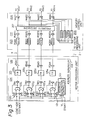
- Figure 5 shows a vector processing system according to an embodiment of the present invention.
- the vector processing system also includes a store data buffer 206 and a buffer controller 207.
- a store access pipe line 102' is started.
- the address generator 103 generates a store address signal in units of vector data elements.
- a plurality of request address signals are supplied to a priority decision circuit 201' in a memory control unit 2' through four address buses 4.
- part of the address data is sent as ID information to the store access processor 104.
- the store access processor 104 reads out data from the vector register unit 105 regardless of priority decision by the priority decision circuit 201'.
- the readout data are aligned, and the aligned data are sent to the store ECC circuit 202 in the memory control unit 2.
- the store data send signal STOREDT is simultaneously supplied to the buffer controller 207 in the memory control unit 2.
- the buffer controller 207 in the memory control unit 2 receives the store data send signal STOREDT from the store access processor 104 in the vector processing unit 1, the buffer controller 207 determines a write address for the store data buffer group 206 and writes the store data in the store data buffer 206.
- the store data read out from the vector register unit 105 are supplied to the corresponding store ECC circuit 202, and the corresponding ECC codes are produced.
- the buffer controller 207 Upon reception of the store data send signal STOREDT from the store access processor 104 in the vector processor unit 1, the buffer controller 207 sends a priority-permission signal PERMPRTY to the priority decision circuit 201 ⁇ .
- the priority decision circuit 201 ⁇ decides the priority of the store for the corresponding vector data element.
- the priority decision circuit 201 ⁇ sends a store request to the main storage unit 3, and simultaneously, a priority signal PRIORITY to the buffer controller 207, so that the store data are read out from the store data buffer 206 and sent to the corresponding main storage units 3.
- FIG. 6 to 8 The detailed circuit arrangement of the vector processing system described above is shown in Figs. 6 to 8.
- the circuit arrangement in Figs. 6 to 8 is an improvement on the arrangement of the circuits shown in Figs. 2 and 3.
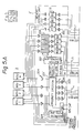
- Figure 6 shows the circuit arrangement of the store access processor 104 ⁇ and relevant circuit thereto in the vector processing unit 1.
- the alignment buffer write register group 111, the alignment buffer unit 112, the write address unit 113, the alignment buffer read register group 114, the read controller 118, and the read address unit 119 in Fig. 2 are omitted from the circuit arrangement in Fig. 6.
- an alignment input register group (AIR) 129 is arranged in place of the alignment buffer read register group 114 in Fig. 2.
- a vector register read controller 109 ⁇ executes read operation of store data at the read timing of the vector register unit when the vector register read controller 109 ⁇ receives a buffer spare signal BUFSPR from the buffer controller 207 in the memory control unit 2.
- Other arrangements of the vector register read controller 109 ⁇ are the same as that Fig. 2.
- the address generator 103 ⁇ includes an identification buffer (IDB) group 127 for temporarily storing ID data which constitutes part of the request address data for the memory control unit 2 and which represents the correspondence between the vector data element and the main storage units 3.
- IDB identification buffer
- the ID data is stored in the ID buffer group 127 at the address generation timing.
- the alignment controller 117 controls the alignment of the store data read out from the vector register unit 105, on the basis of the ID data from the address generator 103 and sends the ID data to the corresponding data buses 5. At the same time, the alignment controller 117 sends the store data send signal STOREDT to the buffer controller 207 in the memory control unit 2 ⁇ .
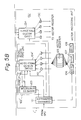
- FIG. 7 A detailed arrangement of the address generator is shown in Fig. 7.
- the address controller 103 in Fig. 7 includes the ID buffer 127, as described above. Since the address pipe line in Fig. 3 is optional, it may be arranged in the circuit of Fig. 7. Other arrangements of the circuit in Fig. 7 are the same as those in Fig. 3.
- the adder unit 122 adds a distance DISTANCE to a lead address LEAD-ADR of each element of the vector data to produce a store address signal for the corresponding main storage units 3.
- the address signal is then transferred to the priority decision circuit 201 in the memory control unit 2 ⁇ through an address translator 125 the request buffer group 203, and the port group 215.
- part of the address data i.e., the ID data for determining which of the main storage units MSU 1 to MSU 4 is accessed, is stored in the ID buffer 127.
- the ID data read out from the ID buffer 127 is sent to the alignment controller 117 in Fig. 6, and the store data is used to determine which main storage unit shall receive the data through the corresponding data bus 5.
- the priority decision circuit 201 ⁇ in the memory control unit 2 ⁇ permits the priority, i.e., the main storage unit initialization, when the store data are written in the store data buffer 206 and the priority permission signal PERMPRTY from the buffer controller 207 is present.
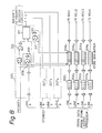
- the circuit arrangement of the buffer controller 207 in the memory control unit 2 ⁇ and its associated circuits are shown in Fig. 8. For illustrative convenience, only the portion for the line A is shown.
- reference numerals 206 denotes the store data buffer; and 207, the buffer controller.
- the buffer controller 207 includes a buffer write control circuit 208, a write address register 209, a store data counter 210, a buffer store data count detector 211, a buffer read control circuit 212, and a read address register 213.
- the arrangement of the buffer controller 207 for the remaining three input lines is the same as that described above.
- Each buffer write control circuit 208 in the buffer controller 207 receives the store data send signal STOREDT upon reception of the corresponding store data from the store access processor 104 ⁇ in the vector processing unit 1 ⁇ .
- the buffer write control circuit 208 receives the store data send signal STOREDT, it generates a write address signal and a write enable signal for the corresponding store data buffer 206.
- the write address signal and the write enable signal are stored in the corresponding store data buffer 206.
- the store data transferred from the store access processor 104 ⁇ in the vector processing unit 1 ⁇ is written at the designated address of the corresponding store data buffer 206.
- the signal STOREDT is counted by the store data counter 210.
- the buffer store data count detector 211 checks the count of the store data counter 210. If the count is not zero, the buffer store data count detector 211 sends the priority permission signal PERMPRTY.
- the priority signal PRIORITY obtained upon decision of the priority by the priority decision circuit 201 ⁇ is supplied to the corresponding buffer read control circuit 212 in the buffer controller 207.
- the control circuit 212 reads out the store data from the store data buffer 206.
- the priority signal PRIORITY is also applied to the store data counter 210, and the counter 210 is decremented.
- the store data counter 210 provides a count obtained by a current difference between the number of data written in the store data buffer 206 and the number of readout data.
- the write address register 209 of the buffer write control circuit 208 and the read address register 213 of the buffer read control circuit 212 store the write and read address signals for the corresponding store data buffer 206. The address is updated every time the read and write access cycle is completed.
- the store data buffer 206 arranged in the memory control unit 2 ⁇ , and the data read out from the vector register unit 105 are subjected to alignment and error checking and correction.
- the resultant data are stored in the corresponding store data buffer in the memory control unit 2 ⁇ .
- the number of store data buffers 206 is equal to the number of main storage units 3.
- the request from the vector processing unit 1 is sent to the memory control unit 2 ⁇ and stored in the request buffer 203 therein.
- the priority decision circuit 201 ⁇ in the memory control unit 2 ⁇ decides the store priority when data is written in the data buffer or data to be written is detected. If the request is permitted, the store data can be immediately transferred to the corresponding main storage units 3. In this case, the minimum data transfer time is the bank busy period.
- the start of the main storage units 3 can be simultaneously performed on a priority basis. Therefore, the bank busy period can be minimized, and processing efficiency can be improved.
- the circuit elements may be arranged in any unit.
- the buffer controller 207 may be arranged in the vector processing unit 1 ⁇ .
- the store data buffers 206 are preferably located near the main storage units 3.
Landscapes
- Engineering & Computer Science (AREA)
- Theoretical Computer Science (AREA)
- Physics & Mathematics (AREA)
- General Engineering & Computer Science (AREA)
- General Physics & Mathematics (AREA)
- Computer Hardware Design (AREA)
- Computing Systems (AREA)
- Complex Calculations (AREA)
Claims (10)
- Système de traitement vectoriel comprenant:
au moins un moyen à mémoire centrale (3);
un moyen de commande de mémoire centrale (2') pour commander l'accès au moyen à mémoire centrale (3);
un moyen de mémorisation de données traitées par traitement vectoriel (105) pour mémoriser des données vectorielles;
un moyen de transfert (102') pour lire les données mémorisées dans le moyen de mémorisation de données traitées par traitement vectoriel (105) et pour transférer ces données jusqu'au moyen de commande de mémoire centrale (2'); et
un moyen de détermination de priorité (201') prévu dans le moyen de commande de mémoire centrale (2') et pour déterminer un ordre de priorité des demandes d'accès au moyen à mémoire centrale (3);
caractérisé en ce que le système comprend en outre:
un moyen à tampons(206) prévu respectivement pour le ou chaque moyen à mémoire centrale (3), connecté activement entre ledit moyen à mémoire centrale et ledit moyen de transfert (102'), pour mémoriser les données qui sont transférées par le moyen de transfert (102') indépendamment de toute décision dudit moyen de détermination de priorité et pour écrire les données dans le moyen à mémoire centrale (3) une fois que la priorité a été déterminée; et
un moyen de commande (207) pour fournir une demande de transfert (PERMPRTY) du moyen de transfert pour le moyen à mémoire centrale (3), au moyen de détermination de priorité (201') quand des données sont déjà mémorisées dans le moyen à tampons(206) ou quand une écriture de données dans le moyen à tampons(206) est identifiée ;
des données pouvant ainsi être transférées directement du moyen à tampons(206) au moyen à mémoire centrale (3) une fois que l'ordre de priorité a été déterminé. - Système de traitement vectoriel selon la revendication 1, dans lequel le moyen de transfert (102') comprend un circuit d'alignement (104') pour aligner lesdites données traitées par traitement vectoriel qui sont lues dans le moyen de mémorisation de données traitées par traitement vectoriel (105) dans un ordre prédéterminé défini par un ordre de mémorisation dans le moyen à mémoire centrale (3), et pour mémoriser lesdites données alignées dans le moyen à tampons(206).
- Système de traitement vectoriel selon la revendication 2, dans lequel ledit moyen de transfert (102') comprend en outre un tampon d'adresses(127) mémorisant une pluralité d'adresses pour indiquer des adresses de mémoire pour ledit moyen à mémoire centrale (3),
ladite lecture de données dans le moyen de mémorisation de données traitées par traitement vectoriel (105) et ledit alignement de données étant effectués en réponse à ladite mémorisation de données desdites adresses de mémoire dans ledit moyen à mémoire centrale (3). - Système de traitement vectoriel selon la revendication 3, dans lequel le moyen à mémoire centrale (3) comprend une pluralité d'unités de mémoire centrale pouvant être mises en fonctionnement indépendamment et le moyen à tampons(206) comprend une pluralité de circuits tampons connectés chacun activement à unedite unité de mémoire centrale correspondante (3), et
dans lequel ledit alignement dans le moyen de transfert (102') est effectué pour satisfaire ledit ordre de mémorisation dans les unités de mémoire centrale. - Système de traitement vectoriel selon la revendication 4, dans lequel le moyen de transfert (102') a une structure pipeline pour exécuter ladite commande en parallèle.
- Système de traitement vectoriel selon la revendication 5, dans lequel le moyen de mémorisation de données traitées par traitement vectoriel (105) comprend en outre un circuit de mémoire pour mémoriser lesdites données traitées par traitement vectoriel.
- Système de traitement vectoriel selon la revendication 6, dans lequel le moyen de mémorisation de données traitées par traitement vectoriel (105) comprend en outre un autre circuit de mémoire pour mémoriser les données à traiter par traitement vectoriel.
- Système de traitement vectoriel selon la revendication 7, dans lequel le moyen de mémorisation de données traitées par traitement vectoriel (105) comprend un circuit de calcul vectoriel pour calculer vectoriellement lesdites données dans ledit autre circuit de mémoire et pour mémoriser lesdites données calculées dans ledit circuit de mémoire.
- Système de traitement vectoriel selon la revendication 8, comprenant en outre un moyen de chargement de données de source, connecté activement entre le moyen à mémoire centrale (3) et le moyen de mémorisation de données traitées par traitement vectoriel (105), pour mémoriser lesdites données de source à calculer vectoriellement dans le moyen à mémoire centrale (3) dans ledit autre circuit de mémoire du moyen de mémorisation de données traitées par traitement vectoriel (105).
- Système de traitement vectoriel selon la revendication 9, dans lequel le moyen de chargement de données de source comprend un autre circuit d'alignement pour aligner lesdites données de source lues dans le moyen à mémoire centrale (3) dans un ordre prédéterminé défini par un ordre de calcul vectoriel dans le moyen de mémorisation de données traitées par traitement vectoriel (105).
Applications Claiming Priority (2)
| Application Number | Priority Date | Filing Date | Title |
|---|---|---|---|
| JP60260858A JPS62120574A (ja) | 1985-11-20 | 1985-11-20 | ベクトル処理装置 |
| JP260858/85 | 1985-11-20 |
Publications (3)
| Publication Number | Publication Date |
|---|---|
| EP0223607A2 EP0223607A2 (fr) | 1987-05-27 |
| EP0223607A3 EP0223607A3 (en) | 1989-09-13 |
| EP0223607B1 true EP0223607B1 (fr) | 1993-02-24 |
Family
ID=17353729
Family Applications (1)
| Application Number | Title | Priority Date | Filing Date |
|---|---|---|---|
| EP86309058A Expired - Lifetime EP0223607B1 (fr) | 1985-11-20 | 1986-11-19 | Système de traitement de vecteurs |
Country Status (5)
| Country | Link |
|---|---|
| US (1) | US4827407A (fr) |
| EP (1) | EP0223607B1 (fr) |
| JP (1) | JPS62120574A (fr) |
| CA (1) | CA1273713A (fr) |
| DE (1) | DE3687822T2 (fr) |
Families Citing this family (12)
| Publication number | Priority date | Publication date | Assignee | Title |
|---|---|---|---|---|
| US5367654A (en) * | 1988-04-13 | 1994-11-22 | Hitachi Ltd. | Method and apparatus for controlling storage in computer system utilizing forecasted access requests and priority decision circuitry |
| DE68924876T2 (de) * | 1988-07-12 | 1996-04-25 | Sony Corp | Integrierte Halbleiterschaltungen. |
| US5432920A (en) * | 1990-04-13 | 1995-07-11 | Hitachi, Ltd. | Store control method with hierarchic priority scheme for computer system |
| JPH0438560A (ja) * | 1990-06-04 | 1992-02-07 | Koufu Nippon Denki Kk | ストアデータ転送方式 |
| US5392443A (en) * | 1991-03-19 | 1995-02-21 | Hitachi, Ltd. | Vector processor with a memory assigned with skewed addresses adapted for concurrent fetching of a number of vector elements belonging to the same vector data |
| US5418973A (en) * | 1992-06-22 | 1995-05-23 | Digital Equipment Corporation | Digital computer system with cache controller coordinating both vector and scalar operations |
| JP3304444B2 (ja) * | 1992-11-30 | 2002-07-22 | 富士通株式会社 | ベクトル処理装置 |
| US6665749B1 (en) * | 1999-08-17 | 2003-12-16 | Nec Electronics, Inc. | Bus protocol for efficiently transferring vector data |
| US6665790B1 (en) | 2000-02-29 | 2003-12-16 | International Business Machines Corporation | Vector register file with arbitrary vector addressing |
| US7308559B2 (en) * | 2000-02-29 | 2007-12-11 | International Business Machines Corporation | Digital signal processor with cascaded SIMD organization |
| US10061746B2 (en) | 2014-09-26 | 2018-08-28 | Intel Corporation | Instruction and logic for a vector format for processing computations |
| WO2022104231A1 (fr) * | 2020-11-16 | 2022-05-19 | Lightmatter, Inc. | Mémorisation de données de processeur vectoriel |
Family Cites Families (20)
| Publication number | Priority date | Publication date | Assignee | Title |
|---|---|---|---|---|
| US3573851A (en) * | 1968-07-11 | 1971-04-06 | Texas Instruments Inc | Memory buffer for vector streaming |
| US4153932A (en) * | 1974-03-29 | 1979-05-08 | Massachusetts Institute Of Technology | Data processing apparatus for highly parallel execution of stored programs |
| JPS5148937A (en) * | 1974-10-25 | 1976-04-27 | Fujitsu Ltd | Kiokusochi niokeru junjoseigyohoshiki |
| US4051551A (en) * | 1976-05-03 | 1977-09-27 | Burroughs Corporation | Multidimensional parallel access computer memory system |
| US4298936A (en) * | 1979-11-15 | 1981-11-03 | Analogic Corporation | Array Processor |
| JPS5725069A (en) * | 1980-07-21 | 1982-02-09 | Hitachi Ltd | Vector data processing equipment |
| US4370732A (en) * | 1980-09-15 | 1983-01-25 | Ibm Corporation | Skewed matrix address generator |
| KR860001434B1 (ko) * | 1980-11-21 | 1986-09-24 | 후지쑤 가부시끼가이샤 | 데이타 처리시 스템 |
| JPS57155666A (en) * | 1981-03-20 | 1982-09-25 | Fujitsu Ltd | Instruction controlling system of vector processor |
| US4594682A (en) * | 1982-12-22 | 1986-06-10 | Ibm Corporation | Vector processing |
| JPS59160267A (ja) * | 1983-03-02 | 1984-09-10 | Hitachi Ltd | ベクトル処理装置 |
| US4697235A (en) * | 1983-03-22 | 1987-09-29 | Fujitsu Limited | List vector control apparatus |
| US4589067A (en) * | 1983-05-27 | 1986-05-13 | Analogic Corporation | Full floating point vector processor with dynamically configurable multifunction pipelined ALU |
| JPS6015771A (ja) * | 1983-07-08 | 1985-01-26 | Hitachi Ltd | ベクトルプロセッサ |
| JPS6069746A (ja) * | 1983-09-26 | 1985-04-20 | Fujitsu Ltd | ベクトル・デ−タ処理装置の制御方式 |
| JPS60134974A (ja) * | 1983-12-23 | 1985-07-18 | Hitachi Ltd | ベクトル処理装置 |
| US4757440A (en) * | 1984-04-02 | 1988-07-12 | Unisys Corporation | Pipelined data stack with access through-checking |
| US4633434A (en) * | 1984-04-02 | 1986-12-30 | Sperry Corporation | High performance storage unit |
| FR2573888B1 (fr) * | 1984-11-23 | 1987-01-16 | Sintra | Systeme pour la transmission simultanee de blocs de donnees ou de vecteurs entre une memoire et une ou plusieurs unites de traitement de donnees |
| US4706191A (en) * | 1985-07-31 | 1987-11-10 | Sperry Corporation | Local store for scientific vector processor |
-
1985
- 1985-11-20 JP JP60260858A patent/JPS62120574A/ja active Pending
-
1986
- 1986-11-17 CA CA000523145A patent/CA1273713A/fr not_active Expired
- 1986-11-19 EP EP86309058A patent/EP0223607B1/fr not_active Expired - Lifetime
- 1986-11-19 US US06/932,324 patent/US4827407A/en not_active Expired - Fee Related
- 1986-11-19 DE DE8686309058T patent/DE3687822T2/de not_active Expired - Fee Related
Also Published As
| Publication number | Publication date |
|---|---|
| EP0223607A2 (fr) | 1987-05-27 |
| DE3687822D1 (de) | 1993-04-01 |
| EP0223607A3 (en) | 1989-09-13 |
| CA1273713C (fr) | 1990-09-04 |
| CA1273713A (fr) | 1990-09-04 |
| US4827407A (en) | 1989-05-02 |
| DE3687822T2 (de) | 1993-06-09 |
| JPS62120574A (ja) | 1987-06-01 |
Similar Documents
| Publication | Publication Date | Title |
|---|---|---|
| US4041472A (en) | Data processing internal communications system having plural time-shared intercommunication buses and inter-bus communication means | |
| US6272596B1 (en) | Data processor | |
| JP3593346B2 (ja) | マルチポートメモリ及びそれをアクセスするデータ処理装置 | |
| EP0223570B1 (fr) | Système de commande d'accès à des vecteurs | |
| JPH0238975B2 (fr) | ||
| US4827407A (en) | Vector processing system | |
| JPS6161436B2 (fr) | ||
| EP0229932B1 (fr) | Mémoire de grande capacité pour systèmes multiprocesseurs | |
| JP2561261B2 (ja) | バッファ記憶アクセス方法 | |
| EP0212152B1 (fr) | Appareil de transfert de mémoire à mémoire assisté par microprocesseur | |
| US5539902A (en) | Vector data processing apparatus wherein a time slot for access to a bank of vector registors is assigned based on memory access time information | |
| EP0067519B1 (fr) | Système de télécommunications | |
| US4737908A (en) | Buffer memory control system | |
| JP3005456B2 (ja) | ベクトル処理装置 | |
| US5822766A (en) | Main memory interface for high speed data transfer | |
| JPH0444136A (ja) | メモリアクセス制御装置 | |
| JP3245488B2 (ja) | リストベクトル処理装置 | |
| JPH01223541A (ja) | インタリーブメモリ装置 | |
| JPS6059621B2 (ja) | バッファ無効化制御方式 | |
| JPH0226259B2 (fr) | ||
| JP2643116B2 (ja) | 主記憶制御装置 | |
| GB2099619A (en) | Data processing arrangements | |
| JPH077388B2 (ja) | ベクトル演算処理装置 | |
| JPH0368045A (ja) | 主記憶制御方式 | |
| JPS58149551A (ja) | 記憶制御方式 |
Legal Events
| Date | Code | Title | Description |
|---|---|---|---|
| PUAI | Public reference made under article 153(3) epc to a published international application that has entered the european phase |
Free format text: ORIGINAL CODE: 0009012 |
|
| AK | Designated contracting states |
Kind code of ref document: A2 Designated state(s): DE FR GB |
|
| PUAL | Search report despatched |
Free format text: ORIGINAL CODE: 0009013 |
|
| AK | Designated contracting states |
Kind code of ref document: A3 Designated state(s): DE FR GB |
|
| 17P | Request for examination filed |
Effective date: 19890927 |
|
| 17Q | First examination report despatched |
Effective date: 19910415 |
|
| GRAA | (expected) grant |
Free format text: ORIGINAL CODE: 0009210 |
|
| AK | Designated contracting states |
Kind code of ref document: B1 Designated state(s): DE FR GB |
|
| PGFP | Annual fee paid to national office [announced via postgrant information from national office to epo] |
Ref country code: FR Payment date: 19930226 Year of fee payment: 8 |
|
| REF | Corresponds to: |
Ref document number: 3687822 Country of ref document: DE Date of ref document: 19930401 |
|
| ET | Fr: translation filed | ||
| PG25 | Lapsed in a contracting state [announced via postgrant information from national office to epo] |
Ref country code: GB Effective date: 19931119 |
|
| PLBE | No opposition filed within time limit |
Free format text: ORIGINAL CODE: 0009261 |
|
| STAA | Information on the status of an ep patent application or granted ep patent |
Free format text: STATUS: NO OPPOSITION FILED WITHIN TIME LIMIT |
|
| 26N | No opposition filed | ||
| GBPC | Gb: european patent ceased through non-payment of renewal fee |
Effective date: 19931119 |
|
| PG25 | Lapsed in a contracting state [announced via postgrant information from national office to epo] |
Ref country code: DE Effective date: 19940802 |
|
| PG25 | Lapsed in a contracting state [announced via postgrant information from national office to epo] |
Ref country code: FR Effective date: 19950731 |
|
| REG | Reference to a national code |
Ref country code: FR Ref legal event code: ST |