EP0223621A2 - Dispositif de mémoire semi-conductrice avec un circuit pour compenser des variations de tension de discrimination dans une cellule de mémoire - Google Patents
Dispositif de mémoire semi-conductrice avec un circuit pour compenser des variations de tension de discrimination dans une cellule de mémoire Download PDFInfo
- Publication number
- EP0223621A2 EP0223621A2 EP86401901A EP86401901A EP0223621A2 EP 0223621 A2 EP0223621 A2 EP 0223621A2 EP 86401901 A EP86401901 A EP 86401901A EP 86401901 A EP86401901 A EP 86401901A EP 0223621 A2 EP0223621 A2 EP 0223621A2
- Authority
- EP
- European Patent Office
- Prior art keywords
- voltage
- memory cell
- compensating
- bit line
- circuit
- Prior art date
- Legal status (The legal status is an assumption and is not a legal conclusion. Google has not performed a legal analysis and makes no representation as to the accuracy of the status listed.)
- Granted
Links
Images


Classifications
-
- G—PHYSICS
- G11—INFORMATION STORAGE
- G11C—STATIC STORES
- G11C11/00—Digital stores characterised by the use of particular electric or magnetic storage elements; Storage elements therefor
- G11C11/21—Digital stores characterised by the use of particular electric or magnetic storage elements; Storage elements therefor using electric elements
- G11C11/34—Digital stores characterised by the use of particular electric or magnetic storage elements; Storage elements therefor using electric elements using semiconductor devices
- G11C11/40—Digital stores characterised by the use of particular electric or magnetic storage elements; Storage elements therefor using electric elements using semiconductor devices using transistors
- G11C11/401—Digital stores characterised by the use of particular electric or magnetic storage elements; Storage elements therefor using electric elements using semiconductor devices using transistors forming cells needing refreshing or charge regeneration, i.e. dynamic cells
- G11C11/4063—Auxiliary circuits, e.g. for addressing, decoding, driving, writing, sensing or timing
- G11C11/407—Auxiliary circuits, e.g. for addressing, decoding, driving, writing, sensing or timing for memory cells of the field-effect type
- G11C11/409—Read-write [R-W] circuits
- G11C11/4099—Dummy cell treatment; Reference voltage generators
-
- G—PHYSICS
- G11—INFORMATION STORAGE
- G11C—STATIC STORES
- G11C11/00—Digital stores characterised by the use of particular electric or magnetic storage elements; Storage elements therefor
- G11C11/21—Digital stores characterised by the use of particular electric or magnetic storage elements; Storage elements therefor using electric elements
- G11C11/34—Digital stores characterised by the use of particular electric or magnetic storage elements; Storage elements therefor using electric elements using semiconductor devices
- G11C11/40—Digital stores characterised by the use of particular electric or magnetic storage elements; Storage elements therefor using electric elements using semiconductor devices using transistors
- G11C11/401—Digital stores characterised by the use of particular electric or magnetic storage elements; Storage elements therefor using electric elements using semiconductor devices using transistors forming cells needing refreshing or charge regeneration, i.e. dynamic cells
- G11C11/4063—Auxiliary circuits, e.g. for addressing, decoding, driving, writing, sensing or timing
- G11C11/407—Auxiliary circuits, e.g. for addressing, decoding, driving, writing, sensing or timing for memory cells of the field-effect type
- G11C11/409—Read-write [R-W] circuits
- G11C11/4094—Bit-line management or control circuits
Definitions
- the present invention relates to a dynamic semiconductor memory device having a circuit for compensating for variations in a discriminating voltage of a memory cell caused by a parasitic capacitance of a gate transistor of the memory cell upon activation thereof.
- the memory capacitor of each memory cell is connected to a bit line through the gate transistor, and a charging stage of the capacitor is detected by a sense amplifier connected to the bit line to discriminate logic "0" or "l" of the memory cell.
- the ON/OFF operation of the gate transistor is performed via a word line.
- the word line may be capacitively coupled to the memory capacitor because of the parasitic capacitance of the gate transistor. If a word line voltage rises to enable the memory cell, the memory cell voltage is influenced by noise through the aforementioned parasitic capacitance and undesirably varies.
- the memory cell discriminating voltage i.e., threshold voltage for discriminating the logic “0” or “l” of the memory cell content
- the margin for noise is reduced and a read error of the memory cell tends to occur.
- a dummy transistor is formed in each memory cell to cancel the parasitic capacitance of the gate transistor by its own parasitic capacitance, hereby variations in discriminating voltage are prevented.
- the dummy transistors are arranged in units of memory cells, the total number of dummy transistors is increased, and a large area is occupied by the dummy transistors in the memory device as a whole. As a result, the memory capacity of the semiconductor memory device per unit area is reduced.
- an object of the present invention to provide a semiconductor memory device having a compensating circuit for compensating for variations in a discriminating voltage of a memory cell caused by noise generated upon activation of a memory cell via a word line, without using a dummy transistor.
- a semiconductor memory device having a circuit for compensating for a discriminating voltage of a memory cell, comprising: a bit line pair consisting of first and second bit lines; a memory cell comprising a memory capacitor for storing data and a gate circuit capable of coupling the memory capacitor to the first bit line of the bit line pair; a word line, connected to the gate circuit, for energizing and deenergizing the gate circuit to control coupling and decoupling of the memory cell to and from the first bit line; a sense amplifier connected to said bit line pair, which sense amplifier being adapted to sense and amplify a voltage at the first bit line by using a precharge voltage of the second bit line as a reference voltage in an active stage of the semiconductor memory device; and a precharge circuit for precharging the bit line pair to a predetermined resultant precharge voltage in a reset state of the semiconductor memory device.
- the precharge circuit precharges the bit line pair with a resultant precharge voltage obtained by adding a compensating voltage to a precharge voltage in the reset state.
- the compensating voltage is adapted to compensate for variation in a memory cell discriminating voltage based on a variation in a memory cell voltage caused by capacitive coupling of the word line to the memory capacitor due to a parasitic capacitance of the gate circuit in the active state.
- the precharge voltage is adapted to optimize the memory cell discriminating voltage when it is assumed that the parasitic capacitance is not present.
- Figure l is a circuit diagram showing conventional semiconductor memory device.
- reference symbols BL and BL(b) denote bit lines; WL, a real word line; MC, a real memory cell; SA, a sense amplifier; Qd, a dummy transistor; and DWL, a dummy word line.
- the memory cell MC comprises a cell capacitor Cs for storing data and a gate transistor Qs for coupling the cell capacitor Cs to the bit line BL.
- Reference symbol PC denotes a cell plate of the cell capacitor Cs, which generates a constant voltage (Vcc/2).
- the sense amplifier SA is a known circuit consisting of transistors Ql, Q2, and Q3.
- Reference symbol Cc denotes a parasitic capacitance existing between the node and the corresponding word line in the memory cell so as to capacitively couple the node to the word line; and Cb, parasitic capacitances of the bit lines BL and BL(b).
- the charged and discharged states of the capacitor Cs in the memory cell MC correspond to logic "l" and logic "0", respectively. If the memory cell is set at logic "l”, a memory cell voltage Vcl is set to be a power source voltage Vcc. However, if the memory cell is set at logic "0", the memory cell voltage Vcl is set to be zero volt. The charging state of the cell capacitor Cs is detected by the sense amplifier SA, thereby reading out data from the memory cell.
- the bit lines BL and BL(b) are precharged at a voltage of Vcc/2, i.e., the accurately intermediate value between the logic "l" and "0" voltages.
- a clock ⁇ 0 is supplied to the sense amplifier SA so that the sense amplifier SA is enabled.
- the voltage at the word line WL rises to turn on the gate transistor Qs so that the cell capacitor Cs is connected to the bit line BL.
- the voltage at the bit line BL is slightly charged up or down with respect to Vcc/2 according to whether the cell capacitor Cs is charged or discharged. The change is detected and amplified by the sense amplifier SA, thereby reading out data from the memory cell.
- the sense amplifier SA uses the precharge voltage of Vcc/2 of the bit line BL(b) as a reference voltage Vrf and detects the change in voltage at the bit line BL. More specifically, if the memory cell MC is set at logic "l", the cell capacitor Cs is discharged to apply a discharge voltage to the bit line BL. In this case, the voltage at the bit line BL is slightly increased from Vcc/2. However, if the memory cell MC is set at logic "0", a charge is supplied from the bit line BL to the cell capacitor Cs so that a voltage at the bit line BL is slightly reduced. This change is detected by the sense amplifier SA using the reference voltage Vrf of Vcc/2.
- Figure 2 is a graph showing the characteristics of equation (2) when the precharge voltage V b (i.e., the reference voltage for causing the sense amplifier SA to discriminate the logic "0" of the memory cell from the logic "l") on the bit lines BL and BL(b) is set to be Vcc/2.
- V b the reference voltage for causing the sense amplifier SA to discriminate the logic "0" of the memory cell from the logic "l"
- the memory cell voltage Vcl is plotted along the abscissa
- the signal magnitude ⁇ V is plotted along the ordinate.
- a solid characteristic curve (a ⁇ represents the characteristics of equation (2).
- the x-intercept of the ⁇ V characteristic curve is the memory cell voltage Vcl as a threshold voltage for discriminating whether the content of the memory cell MC is logic "0" or “l” and is referred to as a discriminating voltage Vds of the memory cell MC.
- the voltage Vcc/2 as a half of a difference (normally Vcc) between the logic "0" and “l" voltages of the memory cell MC is used as the discriminating voltage Vds. If a memory cell voltage Vcl is higher than the discriminating voltage Vds, the corresponding cell is discriminated by the sense amplifier SA to be logic "l”. Otherwise, the memory cell is discriminated to be logic "0", if the memory cell voltage Vcl is lower than the Vds. In this way, a maximum noise margin can be provided to reduce read errors of the memory cell MC.
- the parasitic capacitance Cc for capacitively coupling the memory capacitor Cs and the word line WL is present in the memory cell. Therefore, in practice, the characteristic curve of the signal magnitude ⁇ V is changed as follows.
- an output signal magnitude ⁇ V appearing at the bit line BL under the presence of the coupling parasitic capacitance Cc is given by: since the memory cell voltage in the read mode is given as: Vcl + (Cc/Cs)Vwl
- Equation (7) is represented by a broken characteristic curve (b) in Fig. 2 i.e., a straight line with the following slope, and x- and y-intercepts: Y-intercept:
- the line (b) is obtained by simply parallel displacing the line (a).
- the discriminating voltage Vds of the memory cell MC is represented by equation (9) when the parasitic capacitance Cc is present.
- the dummy cell Qd is connected to the bit line BL to which the memory cell MC is connected, as shown in Fig. l.
- a voltage having a polarity opposite to that of the enabling voltage of the word line WL is applied to the dummy cell Qd through the dummy word line DWL, whereby the potential at the bit line BL is decreased by an increase caused by the parasitic capacitance Cc of the bit line BL, thereby cancelling the influence of the parasitic capacitance Cc.
- the dummy transistor Qd Since the dummy transistor Qd, however, must be arranged in units of memory cells, the total number of dummy transistors in the semiconductor memory device is increased and utilization efficiency of the area of the semiconductor memory cell as a whole is degraded.
- Cps denotes a capacitor for supplying a compensating voltage to bit lines BL and BL(b); Q4, a gate transistor for charging the capacitor Cps in the active state; Q5 and Q6, gate transistors for shunting between the bit lines BL and BL(b) in the reset mode; and Q7, a gate transistor for supplying a charge of the capacitor Cps to the bit lines BL and BL(b) in the reset mode.
- Resistors Rl and R2 serve as voltage dividers for supplying a very-small current to the bit lines so as to prevent the precharge voltage on the bit lines BL and BL(b) from being decreased when the semiconductor memory device is reset for a long period of time, thereby maintaining the bit lines at a predetermined potential (Vcc/2 + ⁇ ).
- the resistors Rl and R2 comprise high-impedance resistors.
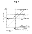
- Figure 4 is a graph wherein the memory cell voltage Vcl of the memory cell MC is plotted along the abscissa and a precharged bit line voltage Vb is plotted along the ordinate.
- the characteristic curves in Fig. 4 represent the memory cell output signal magnitudes ⁇ V as a function of the memory cell voltages Vcl of the memory cell MC when the precharge voltage on the bit lines BL and BL(b) is set at 0, Vcc/2, and Vcc/2 + ⁇ .
- Solid lines (a)1 , (a)2 , and (a)3 are memory cell signal magnitudes ⁇ V when the bit line precharge voltage Vb is set at 0, Vcc/2, and Vcc/2 + ⁇ under the condition that the parasitic capacitance Cc is not present.
- broken lines (b)2 and (b)3 are memory cell signal magnitudes ⁇ V when the bit line precharge voltage Vb is set at Vcc/2 and Vcc/2 + ⁇ under the condition that the parasitic capacitance Cc is actually present.
- a characteristic curve (c) is plotted along bit line voltage points where the signal magnitude ⁇ V becomes 0 for the memory cell voltage Vc, and is represented by a straight line with a slope m of l.
- x (Cc/Cs)Vwl from Vcc/2 when the parasitic capacitance Cc is present.
- the discriminating voltage Vds obtained without the parasitic capacitance Cc is set to be Vcc/2 + x.
- the discriminating voltage Vds is lowered by x, i.e., is set to be Vcc/2.
- the bit line voltage Vb should be set to be If the parasitic capacitance Cc is present, the output signal magnitude ⁇ V is obtained according to the characteristic curve (b)3. In this case, the discriminating voltage Vds of the memory cell MC is properly maintained at Vcc/2, thereby obtaining a maximum operating margin.
- the reference voltage Vrf for discrimination by the sense amplifier is increased or decreased from the normal value (Vcc/2) by a value for compensating a variation ⁇ as an increase or decrease in memory cell voltage Vcl caused by the influence of the parasitic capacitance Cc upon activation of the bit and word lines. Therefore, the discriminating voltage Vds can be maintained at an optimal value.
- bit lines BL and BL(b) are active, one is set at logic “l” (Vcc), and the other is set at logic "0" (0 V).
- the capacitances Cb of the bit lines BL and BL(b) with respect to the ground are the same.
- the gate transistors Q5 and Q6 are turned on to short-circuit the bit lines BL and BL(b), the bit lines BL and BL(b) are precharged at Vcc/2.
- the capacitor Cps having charged by rising the active clock ⁇ a in the active state of the memory device is discharged to the bit lines BL and BL(b), whereby the precharge voltages of the bit lines can be set Vcc/2 + ⁇ higher than Vcc/2.
- An increment ⁇ can be adjusted by the capacitance of the capacitor Cps.
- the capacitor Cps comprises a MOS capacitor so that all capacitors for all bits can be simultaneously formed.
- the occupying area of the MOS capacitors is smaller than that of the dummy cells described with reference to Fig. l, and the MOS capacitors pose little fabrication problems.
- Figure 5 is a time chart for explaining the operation of the embodiment (Fig. 3) of the present invention.
- the same reference numerals as in Fig. 3 denote the same parts in Fig. 5.
- reference symbol SA denotes a timing at which the sense amplifier SA is activated; and AP, an active pull-up timing.
- waveforms at the timing SA are denoted by an enlarged view, wherein BL and BL(b) are waveforms when the cell voltage is high and BL* and BL(b)* when the cell voltage is low.
- an active clock signal ⁇ a is enabled in the active period to charge up the capacitor Cps to Vcc and is disabled in the reset time.
- a clock signal BC2 is enabled to shunt the bit lines so that the bit lines BL and BL(b) and the capacitor Cps are shunted to precharge the bit lines to Vcc/2 + ⁇ .
- the cell plate voltage Vps at the common junction between the resistors Rl and R2 in Fig. 3 is used to set the bit lines BL and BL(b) to the voltage Vcc/2 + ⁇ obtained by voltage division by means of the resistors when the reset time is prolonged.
- reference symbol Q8 denotes a transistor; and ⁇ r , a reset clock signal.
- the reference voltage Vrf is increased to compensate the discriminating voltage Vds decreased by coupling between the work line WL and the node of the memory cell.
- the circuit of Fig. 6 corrects an increase in discriminating voltage.
- the active clock signal ⁇ a and the charge reset signal ⁇ r of the capacitor which has the opposite phase as that of the clock signal ⁇ a are enabled to turn on the transistor Q8 so as to discharge the capacitor Cps during the active period.
- the charge of the capacitor Cps is extracted from the bit lines BL and BL(b) to decrease the reference voltage Vrf. Note that when the transistor Q8 is turned on, the transistor Q4 is turned off.
- one of the electrodes of the capacitor Cps is commonly used as the cell plate of the memory capacitor, a thin-film memory cell can be prepared.
- the reset clock signal ⁇ r in Fig. 6 resets the charged capacitor Cps.
- the reset clock signal ⁇ r is enabled at the same timing as that of the active clock signal ⁇ a and disabled at the reset timing. In this case, the active clock signal ⁇ a is set at low level, and the transistor Q8 is kept off.
- the bit line precharge voltage is derived from the cell plate voltage Vpc.
- the bit line precharge voltage may be provided separately from the cell plate voltage Vpc.
- the cell plate voltage Vpc is preferably set to be about Vcc/2 to reduce a maximum electric field applied to the dielectric members of the capacitor and is not limited to Vcc/2.
Landscapes
- Engineering & Computer Science (AREA)
- Microelectronics & Electronic Packaging (AREA)
- Computer Hardware Design (AREA)
- Dram (AREA)
- Static Random-Access Memory (AREA)
Applications Claiming Priority (2)
| Application Number | Priority Date | Filing Date | Title |
|---|---|---|---|
| JP60222757A JPS6282597A (ja) | 1985-10-08 | 1985-10-08 | 半導体記憶装置 |
| JP222757/85 | 1985-10-08 |
Publications (3)
| Publication Number | Publication Date |
|---|---|
| EP0223621A2 true EP0223621A2 (fr) | 1987-05-27 |
| EP0223621A3 EP0223621A3 (en) | 1990-01-31 |
| EP0223621B1 EP0223621B1 (fr) | 1992-10-28 |
Family
ID=16787430
Family Applications (1)
| Application Number | Title | Priority Date | Filing Date |
|---|---|---|---|
| EP86401901A Expired - Lifetime EP0223621B1 (fr) | 1985-10-08 | 1986-08-29 | Dispositif de mémoire semi-conductrice avec un circuit pour compenser des variations de tension de discrimination dans une cellule de mémoire |
Country Status (5)
| Country | Link |
|---|---|
| US (1) | US4716549A (fr) |
| EP (1) | EP0223621B1 (fr) |
| JP (1) | JPS6282597A (fr) |
| KR (1) | KR900002667B1 (fr) |
| DE (1) | DE3687037T2 (fr) |
Cited By (1)
| Publication number | Priority date | Publication date | Assignee | Title |
|---|---|---|---|---|
| WO1997023875A1 (fr) * | 1995-12-22 | 1997-07-03 | Micron Technology, Inc. | Memoire dram a detection par un circuit de reference du bord d'une matrice memoire |
Families Citing this family (9)
| Publication number | Priority date | Publication date | Assignee | Title |
|---|---|---|---|---|
| JPS63308792A (ja) * | 1987-06-10 | 1988-12-16 | Mitsubishi Electric Corp | 半導体記憶装置 |
| JPH01171194A (ja) * | 1987-12-25 | 1989-07-06 | Nec Ic Microcomput Syst Ltd | 半導体記憶装置 |
| US5687109A (en) * | 1988-05-31 | 1997-11-11 | Micron Technology, Inc. | Integrated circuit module having on-chip surge capacitors |
| KR930000899B1 (ko) * | 1990-02-24 | 1993-02-11 | 현대전자산업 주식회사 | 다이나믹 램(dram)의 비트선 센스 증폭기의 균형 실현장치 |
| US5135889A (en) * | 1991-12-09 | 1992-08-04 | Micron Technology, Inc. | Method for forming a shielding structure for decoupling signal traces in a semiconductor |
| EP0663667B1 (fr) * | 1994-01-12 | 1999-03-03 | Siemens Aktiengesellschaft | Circuit intégré de mémoire à semi-conducteurs, et méthode d'opération |
| JP2748873B2 (ja) * | 1995-01-04 | 1998-05-13 | 日本電気株式会社 | 強誘電体メモリ装置およびその動作制御方法 |
| US10541031B2 (en) | 2018-06-15 | 2020-01-21 | Sandisk Technologies Llc | Single pulse SLC programming scheme |
| US10825513B2 (en) | 2018-06-26 | 2020-11-03 | Sandisk Technologies Llc | Parasitic noise control during sense operations |
Family Cites Families (6)
| Publication number | Priority date | Publication date | Assignee | Title |
|---|---|---|---|---|
| US3909631A (en) * | 1973-08-02 | 1975-09-30 | Texas Instruments Inc | Pre-charge voltage generating system |
| US3946368A (en) * | 1974-12-27 | 1976-03-23 | Intel Corporation | System for compensating voltage for a CCD sensing circuit |
| DE2647394C2 (de) * | 1976-10-20 | 1978-11-16 | Siemens Ag, 1000 Berlin Und 8000 Muenchen | MOS-Halbleiterspeicherbaustein |
| JPS5939833B2 (ja) * | 1977-05-24 | 1984-09-26 | 日本電気株式会社 | センス増幅器 |
| JPS6044752B2 (ja) * | 1978-04-24 | 1985-10-05 | 日本電気株式会社 | ダイナミツクメモリ |
| EP0189908B1 (fr) * | 1985-01-30 | 1992-10-28 | Nec Corporation | Mémoire dynamique comprenant un dispositif pour la précharge de lignes de bit |
-
1985
- 1985-10-08 JP JP60222757A patent/JPS6282597A/ja active Granted
-
1986
- 1986-08-29 EP EP86401901A patent/EP0223621B1/fr not_active Expired - Lifetime
- 1986-08-29 US US06/901,680 patent/US4716549A/en not_active Expired - Fee Related
- 1986-08-29 DE DE8686401901T patent/DE3687037T2/de not_active Expired - Fee Related
- 1986-09-01 KR KR8607289A patent/KR900002667B1/ko not_active Expired
Cited By (4)
| Publication number | Priority date | Publication date | Assignee | Title |
|---|---|---|---|---|
| WO1997023875A1 (fr) * | 1995-12-22 | 1997-07-03 | Micron Technology, Inc. | Memoire dram a detection par un circuit de reference du bord d'une matrice memoire |
| US5726931A (en) * | 1995-12-22 | 1998-03-10 | Micron Technology, Inc. | DRAM with open digit lines and array edge reference sensing |
| US5844833A (en) * | 1995-12-22 | 1998-12-01 | Micron Technology, Inc. | DRAM with open digit lines and array edge reference sensing |
| KR100304506B1 (ko) * | 1995-12-22 | 2001-11-22 | 로데릭 더블류 루이스 | 어레이에지기준감지동작을수행하는dram |
Also Published As
| Publication number | Publication date |
|---|---|
| JPS6282597A (ja) | 1987-04-16 |
| JPH0468716B2 (fr) | 1992-11-04 |
| DE3687037D1 (de) | 1992-12-03 |
| KR870004447A (ko) | 1987-05-09 |
| EP0223621A3 (en) | 1990-01-31 |
| DE3687037T2 (de) | 1993-03-11 |
| KR900002667B1 (en) | 1990-04-21 |
| US4716549A (en) | 1987-12-29 |
| EP0223621B1 (fr) | 1992-10-28 |
Similar Documents
| Publication | Publication Date | Title |
|---|---|---|
| KR100444116B1 (ko) | 강유전체 메모리 | |
| EP0473360B1 (fr) | Dispositif de mémoire à semi-conducteurs | |
| US4932002A (en) | Bit line latch sense amp | |
| US4351034A (en) | Folded bit line-shared sense amplifiers | |
| EP0080935B1 (fr) | Dispositif de mémoire semi-conductrice dynamique | |
| KR910009442B1 (ko) | 반도체 기억장치 | |
| KR20000029138A (ko) | 연상 메모리(cam) | |
| EP0833340B1 (fr) | Circuit de lecture pour cellules mémoires à semi-conducteur | |
| EP0223621B1 (fr) | Dispositif de mémoire semi-conductrice avec un circuit pour compenser des variations de tension de discrimination dans une cellule de mémoire | |
| US4458336A (en) | Semiconductor memory circuit | |
| US4338679A (en) | Row driver circuit for semiconductor memory | |
| EP0073677B1 (fr) | Circuit de transistor MIS comprenant un circuit de maintien de tension | |
| US4907200A (en) | Dynamic memory | |
| KR100275109B1 (ko) | 강유전체메모리장치및그동작방법 | |
| US4404661A (en) | Semiconductor memory circuit | |
| US4733373A (en) | Dynamic memory with improved arrangement for precharging bit lines | |
| US4484312A (en) | Dynamic random access memory device | |
| USRE32682E (en) | Folded bit line-shared sense amplifiers | |
| JPH0217874B2 (fr) | ||
| JP2555156B2 (ja) | ダイナミックram | |
| US5940338A (en) | Memory device with a sense amplifier | |
| EP0318094B1 (fr) | Circuit de mémorisation intégré à réglage interne de la tension d'alimentation | |
| EP0068894B1 (fr) | Dispositif de mémoire dynamique à accès aléatoire | |
| JPH11260060A (ja) | ランダム・アクセス・メモリ | |
| US20020000839A1 (en) | Sense amplifier |
Legal Events
| Date | Code | Title | Description |
|---|---|---|---|
| PUAI | Public reference made under article 153(3) epc to a published international application that has entered the european phase |
Free format text: ORIGINAL CODE: 0009012 |
|
| AK | Designated contracting states |
Kind code of ref document: A2 Designated state(s): DE FR GB |
|
| PUAL | Search report despatched |
Free format text: ORIGINAL CODE: 0009013 |
|
| AK | Designated contracting states |
Kind code of ref document: A3 Designated state(s): DE FR GB |
|
| 17P | Request for examination filed |
Effective date: 19900716 |
|
| 17Q | First examination report despatched |
Effective date: 19910412 |
|
| GRAA | (expected) grant |
Free format text: ORIGINAL CODE: 0009210 |
|
| PGFP | Annual fee paid to national office [announced via postgrant information from national office to epo] |
Ref country code: FR Payment date: 19921006 Year of fee payment: 8 |
|
| AK | Designated contracting states |
Kind code of ref document: B1 Designated state(s): DE FR GB |
|
| REF | Corresponds to: |
Ref document number: 3687037 Country of ref document: DE Date of ref document: 19921203 |
|
| ET | Fr: translation filed | ||
| PLBE | No opposition filed within time limit |
Free format text: ORIGINAL CODE: 0009261 |
|
| STAA | Information on the status of an ep patent application or granted ep patent |
Free format text: STATUS: NO OPPOSITION FILED WITHIN TIME LIMIT |
|
| PG25 | Lapsed in a contracting state [announced via postgrant information from national office to epo] |
Ref country code: GB Effective date: 19930829 |
|
| 26N | No opposition filed | ||
| GBPC | Gb: european patent ceased through non-payment of renewal fee |
Effective date: 19930829 |
|
| PG25 | Lapsed in a contracting state [announced via postgrant information from national office to epo] |
Ref country code: FR Effective date: 19940429 |
|
| PG25 | Lapsed in a contracting state [announced via postgrant information from national office to epo] |
Ref country code: DE Effective date: 19940503 |
|
| REG | Reference to a national code |
Ref country code: FR Ref legal event code: ST |