EP0223702A1 - Gewichtete Bilanz und Analog-Digital-Wandler, welcher eine solche Bilanz benutzt - Google Patents
Gewichtete Bilanz und Analog-Digital-Wandler, welcher eine solche Bilanz benutzt Download PDFInfo
- Publication number
- EP0223702A1 EP0223702A1 EP86402507A EP86402507A EP0223702A1 EP 0223702 A1 EP0223702 A1 EP 0223702A1 EP 86402507 A EP86402507 A EP 86402507A EP 86402507 A EP86402507 A EP 86402507A EP 0223702 A1 EP0223702 A1 EP 0223702A1
- Authority
- EP
- European Patent Office
- Prior art keywords
- transistor
- balance
- drain
- analog
- transistors
- Prior art date
- Legal status (The legal status is an assumption and is not a legal conclusion. Google has not performed a legal analysis and makes no representation as to the accuracy of the status listed.)
- Granted
Links
- 238000005259 measurement Methods 0.000 claims abstract description 13
- 230000005669 field effect Effects 0.000 claims description 9
- 230000005533 two-dimensional electron gas Effects 0.000 claims description 3
- 238000010586 diagram Methods 0.000 description 6
- 238000005070 sampling Methods 0.000 description 3
- 235000021183 entrée Nutrition 0.000 description 2
- 238000012545 processing Methods 0.000 description 2
- JBRZTFJDHDCESZ-UHFFFAOYSA-N AsGa Chemical compound [As]#[Ga] JBRZTFJDHDCESZ-UHFFFAOYSA-N 0.000 description 1
- 229910001218 Gallium arsenide Inorganic materials 0.000 description 1
- 241001080024 Telles Species 0.000 description 1
- 240000008042 Zea mays Species 0.000 description 1
- 230000006978 adaptation Effects 0.000 description 1
- 230000000903 blocking effect Effects 0.000 description 1
- 238000006243 chemical reaction Methods 0.000 description 1
- 230000000295 complement effect Effects 0.000 description 1
- 238000013461 design Methods 0.000 description 1
- 238000004519 manufacturing process Methods 0.000 description 1
- 238000001465 metallisation Methods 0.000 description 1
- 238000012552 review Methods 0.000 description 1
- 230000001360 synchronised effect Effects 0.000 description 1
Images
Classifications
-
- H—ELECTRICITY
- H03—ELECTRONIC CIRCUITRY
- H03K—PULSE TECHNIQUE
- H03K3/00—Circuits for generating electric pulses; Monostable, bistable or multistable circuits
- H03K3/02—Generators characterised by the type of circuit or by the means used for producing pulses
- H03K3/353—Generators characterised by the type of circuit or by the means used for producing pulses by the use, as active elements, of field-effect transistors with internal or external positive feedback
- H03K3/356—Bistable circuits
- H03K3/356017—Bistable circuits using additional transistors in the input circuit
- H03K3/356026—Bistable circuits using additional transistors in the input circuit with synchronous operation
-
- H—ELECTRICITY
- H03—ELECTRONIC CIRCUITRY
- H03M—CODING; DECODING; CODE CONVERSION IN GENERAL
- H03M1/00—Analogue/digital conversion; Digital/analogue conversion
- H03M1/12—Analogue/digital converters
- H03M1/34—Analogue value compared with reference values
- H03M1/36—Analogue value compared with reference values simultaneously only, i.e. parallel type
- H03M1/361—Analogue value compared with reference values simultaneously only, i.e. parallel type having a separate comparator and reference value for each quantisation level, i.e. full flash converter type
- H03M1/366—Analogue value compared with reference values simultaneously only, i.e. parallel type having a separate comparator and reference value for each quantisation level, i.e. full flash converter type using current mode circuits, i.e. circuits in which the information is represented by current values rather than by voltage values
Definitions
- the present invention relates to a calibrated weight balance, intended for the production of very high speed analog-to-digital converters.
- This balance uses a Schmitt flip-flop made up of normally blocked transistors, the dimensions of which are calculated so that the flip-flop changes state as a function of the value of the input signal relative to the value of one of the two resistors of transistor drain, which is precisely the resistance of calibrated weight.
- Analog-to-digital converters are widely used in all equipment for processing analog signals transmitted by air or by coaxial cable, but they are a weak point in the signal processing chain due to their relative slowness.
- terrestrial satellites for example, are equipped with electronic systems operating at several gigahertz, or while other equipment takes advantage of the transparency of the atmosphere at 94 GHz
- the analog-to-digital converters with medium resolution currently known. have a speed of the order of 500 MHz.
- the calibrated weight balance according to the invention makes it possible to produce analog-digital converters which operate at more than 2 GHz , for a resolution of 5 or 6 bits for example.
- the balance according to the invention consists of a Schmitt bistable flip-flop, the two field effect transistors of which are supplied by a third transistor, operating as a current source, itself controlled by a clock signal at through an inverter called DCFL -Direct Coupled FET Logic-.
- a first transistor of the bistable flip-flop constitutes the reference channel: mounted source to ground, its drain is connected to the central point of a divider constituted by a resistor connected to ground and by a resistor connected to the current source: these two resistors are fixed.
- a second transistor of the flip-flop constitutes the measurement channel: mounted source to ground, its drain is connected to the central point of a divider constituted by a resistor connected to the current source, and by a third transistor, whose source is connected to a reference voltage.
- the analog input signal is applied to the gate of this third transistor, and the supply resistance of the measurement channel constitutes the calibrated weight of the balance according to the invention.
- the two complementary outputs of the balance are taken from the drains of the two transistors of the flip-flop: depending on the value of the analog signal applied to the gate of the third transistor, one of these two outputs is at logic level 1 and the other at logical level 0, or vice versa.
- each balance is characterized by its resistance in series with the third transistor: this has a value which depends on the rank of the balance in the converter.
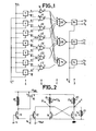
- Figure 1 shows the diagram of such a converter.
- An analog-digital converter comprises, in a known manner, four stages which are identified by the letters A to D in Figure 1.
- the first stage A is constituted by a series of balances 1 to 7, each of which receives, in parallel inputs, an input signal V E , analog, and a clock signal H.
- the number of scales which here is 7, does not limit the scope of the invention, but is linked to the resolution of the converter, and to the number of bits at output: 2N - 1 scales are required for a digitized signal of N bits.
- the first output of the first balance 1 is not used for measurement, and is not connected to an YES-NO door.
- the second output Q of the last balance 7 is connected to a simple inverter 72, since an ON / OFF gate is not useful if it only works on one input.
- the fourth stage D consists of N flip-flops D 14, 24, 34 if there are N bits. All these flip-flops D have their input combined at the output of an OU-NON gate of the preceding stage, and are synchronized by the same clock signal H as the balances of the first stage: they deliver the digitized signals on their outputs S and: 3 bits in the example illustrated.
- the binary number provided by the second encoder, or third stage C, is recorded in the shift register constituted by the fourth stage D. Synchronization by the sampling clock H allows the analog-digital converter to carry out a new sampling , on the first stage of scales, without losing the acquisition of the previous one, stored in the shift register.
- Such a converter is known as a "flash" converter: it is much faster than converters using sample-and-hold units and counters.
- the calibrated weight balance is organized around a bistable rocker, i.e. two crossed logic inverters, formed by two field effect transistors 15 and 16 and two resistors 25 and 26.
- the transistors 15 and 16 are connected to ground by their source and resistors 25 and 26, respectively, by their drain.
- the opposite ends of these resistors 25 and 26 are joined together to a programmed current source.
- the programmed current source consists of a field effect transistor 18, the drain of which is connected to a voltage + V DD and the source of which is connected to the two resistors 25 and 26 mentioned above.
- the gate of transistor 18 is controlled by the output of a DCFL inverter formed by a transistor 19 and a resistor 28, both of which are connected between ground and voltage + V DD .
- a clock signal H is applied to the gate of the transistor 19 of the inverter: it is therefore it which synchronizes the current source 18, and programs the operation of the balance.
- the two transistors 15 and 16 of the flip-flop operate one in the reference channel, the other in the measurement channel to "weigh" the analog input signal.
- the reference channel is formed by a first transistor 15, the drain of which is connected to the common point between the resistor 25 of the inverter, already mentioned, and a third resistor 27, connected to ground by its other end.
- the measurement channel is formed by a second transistor 16, the drain of which is connected to the common point between the resistor 26 of the inverter, already mentioned, and the drain of a third transistor 17, the source of which is connected to a voltage of negative reference -Vref, whose function will be explained later.
- the gate of this third transistor 17 constitutes the input of the balance according to the invention: an analog voltage Ve is applied to it.
- the additional Q and balance outputs are taken from the drains of the first and second transistors 15 and 16.
- the components which "weigh" the analog input signal V E are the three resistors 25, 26, 27 and the third transistor 17.
- the first and third resistors 25 and 27 are of fixed value, and common to all the balances of an analog-to-digital converter. They are dimensioned in such a way that, la being the reference current which crosses the resistor 27, the resistor 25 is crossed by a current 21 0 .
- the second resistor 26 has a value which depends on the rank M of a balance in an analog-digital converter, it is crossed by a current (M + 1) I 0 for a balance of rank M. It is this which constitutes the calibrated weight of the scale.
- the transistor 17 which has the same characteristics for all the balances of a converter, but whose current varies with the signal to be measured V E , constitutes with the resistor 26 a variable measurement scale, as opposed to the measurement scale fixed formed by fixed resistors 25 and 27.
- All the resistors 25, 26, 27 of the flip-flop and even 28 of the current source are resistors of the saturable current type, that is to say transistors without a grid, or transistors with a channel dug in the active layer, or else transistors in which holes are dug in the active layer, under the gate metallization. All these types of saturable charges are well known.
- the first condition limits the input voltages V E as a function of the reference voltage Vref. This is why the source of the third transistor 17 is connected to a negative reference voltage -Vref. It is an adaptation voltage, which makes it possible to convert analog signals whose input voltage V E is lower than the threshold voltage V T of the transistors, which are all normally blocked.
- the second condition ensures the blocking of the transistor 15 before switching: for the balance to "weigh" an input signal, the reference branch of the balance must not have been originally modified by a transistor 15 made conductive. This is also the reason why all the transistors of the balance are of the normally blocked type.
- G m being the transconductance
- the first case corresponds to a sampling of logic signals between V T (0 logic) and 2V T (1 logic).
- the second case corresponds to the coding of signals between 0 and a maximum of 2V T.
- the third case corresponds to the alternating signals between -2V T and + 2V T.
- the dimensions of the transistor 17 are determined as a function of its transcductance G m , of the current I 0 and of the number N of binary bits of the converter, knowing that:
- thermometer scale into a point scale
- the first encoder therefore provides a point scale.
- This scale of points is transformed into a binary number by means of the second encoder of doors OU-NON 13, 23 and 33 and of the shift register of rockers D 14, 24 and 34, if one codes with 3 bits.
- the number of gates and flip-flops D is modified accordingly.
- each output of the second encoder follows the points where the output of the first encoder is 1. We see that, for example, 7 "weighs" the same weight as 6 + 1 or that 5 + 2 or that 4 + 3.
- the output So comes from levels 1, 3, 5 and 7, i.e. doors 12, 32, 52, 72.
- the output Si comes from levels 2, 3, 6 and 7, i.e. doors 22, 32, 62, 72.
- the output S 2 comes from levels 4, 5, 6 and 7, i.e. doors 42, 52, 62, 72.
- the calibrated weight balance of the invention is applied in systems which require rapid analog-to-digital conversion, such as measuring devices or multiplexer-demultiplexers for satellite communications.
- the electron gas heterojunction transistors give it a high operating speed, greater than 2 GHz, but of course the scale diagram remains valid if it is made with other transistors, or if conventional variants are applied to it for those skilled in the art. It is specified by the following claims.
Landscapes
- Engineering & Computer Science (AREA)
- Theoretical Computer Science (AREA)
- Analogue/Digital Conversion (AREA)
Applications Claiming Priority (2)
| Application Number | Priority Date | Filing Date | Title |
|---|---|---|---|
| FR8516933A FR2590427B1 (fr) | 1985-11-15 | 1985-11-15 | Balance a poids etalonne, et convertisseur analogique-numerique utilisant une telle balance |
| FR8516933 | 1985-11-15 |
Publications (2)
| Publication Number | Publication Date |
|---|---|
| EP0223702A1 true EP0223702A1 (de) | 1987-05-27 |
| EP0223702B1 EP0223702B1 (de) | 1990-04-11 |
Family
ID=9324864
Family Applications (1)
| Application Number | Title | Priority Date | Filing Date |
|---|---|---|---|
| EP86402507A Expired - Lifetime EP0223702B1 (de) | 1985-11-15 | 1986-11-12 | Gewichtete Bilanz und Analog-Digital-Wandler, welcher eine solche Bilanz benutzt |
Country Status (5)
| Country | Link |
|---|---|
| US (1) | US4739306A (de) |
| EP (1) | EP0223702B1 (de) |
| CA (1) | CA1257394A (de) |
| DE (1) | DE3670409D1 (de) |
| FR (1) | FR2590427B1 (de) |
Cited By (1)
| Publication number | Priority date | Publication date | Assignee | Title |
|---|---|---|---|---|
| US5141811A (en) * | 1989-12-01 | 1992-08-25 | Teijin Limited | Elastic synthetic polymer filament with multi-lobated cross-sectional profile |
Families Citing this family (2)
| Publication number | Priority date | Publication date | Assignee | Title |
|---|---|---|---|---|
| US5072221A (en) * | 1988-08-04 | 1991-12-10 | Signal Processing Technologies, Inc. | Error limiting analog to digital converter |
| US5045680A (en) * | 1990-01-18 | 1991-09-03 | International Business Machines Corporation | Integrated circuit optoelectronic toggle F/F |
Citations (1)
| Publication number | Priority date | Publication date | Assignee | Title |
|---|---|---|---|---|
| US4291246A (en) * | 1979-03-05 | 1981-09-22 | Motorola Inc. | Differential capacitive buffer |
Family Cites Families (1)
| Publication number | Priority date | Publication date | Assignee | Title |
|---|---|---|---|---|
| JPS57199322A (en) * | 1981-06-01 | 1982-12-07 | Seiko Instr & Electronics Ltd | Ad converter |
-
1985
- 1985-11-15 FR FR8516933A patent/FR2590427B1/fr not_active Expired
-
1986
- 1986-11-07 US US06/927,724 patent/US4739306A/en not_active Expired - Fee Related
- 1986-11-12 EP EP86402507A patent/EP0223702B1/de not_active Expired - Lifetime
- 1986-11-12 DE DE8686402507T patent/DE3670409D1/de not_active Expired - Fee Related
- 1986-11-14 CA CA000522974A patent/CA1257394A/fr not_active Expired
Patent Citations (1)
| Publication number | Priority date | Publication date | Assignee | Title |
|---|---|---|---|---|
| US4291246A (en) * | 1979-03-05 | 1981-09-22 | Motorola Inc. | Differential capacitive buffer |
Non-Patent Citations (2)
| Title |
|---|
| PATENTS ABSTRACTS OF JAPAN, vol. 7, no. 49 (E-16)[1194], 24 février 1983, page 116 E 161; & JP-A-57 199 322 (DAINI SEIKOSHA K.K.) 07-12-1982 * |
| RCA REVIEW, vol. 41, juin 1980, pages 198-212, Princeton, US; L.C. UPADHYAYULA: "GaAs MESFET comparators for gigabit-rate analog-to-digital converters" * |
Cited By (1)
| Publication number | Priority date | Publication date | Assignee | Title |
|---|---|---|---|---|
| US5141811A (en) * | 1989-12-01 | 1992-08-25 | Teijin Limited | Elastic synthetic polymer filament with multi-lobated cross-sectional profile |
Also Published As
| Publication number | Publication date |
|---|---|
| FR2590427B1 (fr) | 1987-12-18 |
| US4739306A (en) | 1988-04-19 |
| FR2590427A1 (fr) | 1987-05-22 |
| EP0223702B1 (de) | 1990-04-11 |
| DE3670409D1 (de) | 1990-05-17 |
| CA1257394A (fr) | 1989-07-11 |
Similar Documents
| Publication | Publication Date | Title |
|---|---|---|
| FR2508659A1 (fr) | Procede et dipositif optique de conversion analogique-numerique | |
| EP1085659A1 (de) | Digital-Analog-Wandler des Stromtyps | |
| FR2689339A1 (fr) | Procédé et dispositif de réglage de retard à plusieurs gammes. | |
| FR2800938A1 (fr) | Circuit d'excitation de commutation, circuit de commutation utilisant un tel circuit d'excitation, et circuit convertisseur numerique-analogique utilisant ce circuit de commutation | |
| FR2497615A1 (fr) | Dispositif de transmission de signaux presentant une caracteristique de transmission reglable pas a pas | |
| EP0223702B1 (de) | Gewichtete Bilanz und Analog-Digital-Wandler, welcher eine solche Bilanz benutzt | |
| FR2550671A1 (fr) | Circuit convertisseur analogique-numerique et demodulateur de signaux video modules en argument | |
| EP0194195A1 (de) | Statische bistabile Kippschaltung in CMOS-Technologie | |
| EP0905907B1 (de) | Exklusiv-Oder-Gatter mit vier zwei-zu-zwei komplementären Eingängen und zwei komplementären Ausgängen sowie Frequenzmultiplizierer damit | |
| EP1690337B1 (de) | Schneller analog-digital-umsetzer | |
| EP1925079B1 (de) | Stromschalter mit durch eine niederspannung gespeisten differenztransistorpaaren | |
| FR2484173A1 (fr) | Circuit logique supraconducteur | |
| FR2648643A1 (fr) | Circuit d'interface entre deux circuits numeriques de natures differentes | |
| EP0200255B1 (de) | Schaltstufe einer Darlington-Type insbesondere für Speicher-Wortzeile-Dekodierer | |
| EP0246135B1 (de) | Phasen- und Frequenzdetektor und seine Anwendung in einer Phasenregelschleife | |
| EP0203645B1 (de) | Integrierte Digital/Analog-Wandlerschaltung mit Gerät zur Glitchreduzierung | |
| CA2146196A1 (fr) | Circuit a retard reglable | |
| EP0140413A2 (de) | Dekodierschaltung für statischen RAM-Speicher | |
| FR2572574A1 (fr) | Cellule de memoire de registre a decalage | |
| EP0169089B1 (de) | Elementare Datenverarbeitungsvorrichtung | |
| EP3182617B1 (de) | Optischer empfänger mit relativer phasendetektion | |
| EP0155046A1 (de) | Gerät zur Digital-Analogwandlung | |
| EP3888248A1 (de) | Vorrichtung zur erzeugung von analogen signalen | |
| FR2633051A1 (fr) | Circuit comparateur a verrouillage | |
| EP0760180B1 (de) | Verfahren und einrichtung für pseudozufallsschalten |
Legal Events
| Date | Code | Title | Description |
|---|---|---|---|
| PUAI | Public reference made under article 153(3) epc to a published international application that has entered the european phase |
Free format text: ORIGINAL CODE: 0009012 |
|
| AK | Designated contracting states |
Kind code of ref document: A1 Designated state(s): DE GB IT NL |
|
| 17P | Request for examination filed |
Effective date: 19870609 |
|
| 17Q | First examination report despatched |
Effective date: 19890315 |
|
| RAP3 | Party data changed (applicant data changed or rights of an application transferred) |
Owner name: THOMSON-CSF |
|
| GRAA | (expected) grant |
Free format text: ORIGINAL CODE: 0009210 |
|
| AK | Designated contracting states |
Kind code of ref document: B1 Designated state(s): DE GB IT NL |
|
| ITF | It: translation for a ep patent filed | ||
| REF | Corresponds to: |
Ref document number: 3670409 Country of ref document: DE Date of ref document: 19900517 |
|
| GBT | Gb: translation of ep patent filed (gb section 77(6)(a)/1977) | ||
| PLBE | No opposition filed within time limit |
Free format text: ORIGINAL CODE: 0009261 |
|
| STAA | Information on the status of an ep patent application or granted ep patent |
Free format text: STATUS: NO OPPOSITION FILED WITHIN TIME LIMIT |
|
| 26N | No opposition filed | ||
| ITTA | It: last paid annual fee | ||
| PGFP | Annual fee paid to national office [announced via postgrant information from national office to epo] |
Ref country code: NL Payment date: 19951013 Year of fee payment: 10 |
|
| PGFP | Annual fee paid to national office [announced via postgrant information from national office to epo] |
Ref country code: GB Payment date: 19951020 Year of fee payment: 10 |
|
| PGFP | Annual fee paid to national office [announced via postgrant information from national office to epo] |
Ref country code: DE Payment date: 19951021 Year of fee payment: 10 |
|
| PG25 | Lapsed in a contracting state [announced via postgrant information from national office to epo] |
Ref country code: GB Effective date: 19961112 |
|
| PG25 | Lapsed in a contracting state [announced via postgrant information from national office to epo] |
Ref country code: NL Effective date: 19970601 |
|
| GBPC | Gb: european patent ceased through non-payment of renewal fee |
Effective date: 19961112 |
|
| NLV4 | Nl: lapsed or anulled due to non-payment of the annual fee |
Effective date: 19970601 |
|
| PG25 | Lapsed in a contracting state [announced via postgrant information from national office to epo] |
Ref country code: DE Effective date: 19970801 |
|
| PG25 | Lapsed in a contracting state [announced via postgrant information from national office to epo] |
Ref country code: IT Free format text: LAPSE BECAUSE OF NON-PAYMENT OF DUE FEES;WARNING: LAPSES OF ITALIAN PATENTS WITH EFFECTIVE DATE BEFORE 2007 MAY HAVE OCCURRED AT ANY TIME BEFORE 2007. THE CORRECT EFFECTIVE DATE MAY BE DIFFERENT FROM THE ONE RECORDED. Effective date: 20051112 |