EP0905907B1 - Exklusiv-Oder-Gatter mit vier zwei-zu-zwei komplementären Eingängen und zwei komplementären Ausgängen sowie Frequenzmultiplizierer damit - Google Patents
Exklusiv-Oder-Gatter mit vier zwei-zu-zwei komplementären Eingängen und zwei komplementären Ausgängen sowie Frequenzmultiplizierer damit Download PDFInfo
- Publication number
- EP0905907B1 EP0905907B1 EP98402263A EP98402263A EP0905907B1 EP 0905907 B1 EP0905907 B1 EP 0905907B1 EP 98402263 A EP98402263 A EP 98402263A EP 98402263 A EP98402263 A EP 98402263A EP 0905907 B1 EP0905907 B1 EP 0905907B1
- Authority
- EP
- European Patent Office
- Prior art keywords
- type
- branch
- transistors
- inputs
- branches
- Prior art date
- Legal status (The legal status is an assumption and is not a legal conclusion. Google has not performed a legal analysis and makes no representation as to the accuracy of the status listed.)
- Expired - Lifetime
Links
- 230000000295 complement effect Effects 0.000 title claims description 46
- 238000005070 sampling Methods 0.000 claims description 5
- 238000005516 engineering process Methods 0.000 description 10
- 230000007704 transition Effects 0.000 description 10
- 235000021183 entrée Nutrition 0.000 description 5
- 239000000758 substrate Substances 0.000 description 5
- 230000005540 biological transmission Effects 0.000 description 4
- 230000000694 effects Effects 0.000 description 4
- 230000008901 benefit Effects 0.000 description 3
- 230000008859 change Effects 0.000 description 3
- 230000004044 response Effects 0.000 description 3
- 230000003068 static effect Effects 0.000 description 3
- 239000000969 carrier Substances 0.000 description 2
- 230000003071 parasitic effect Effects 0.000 description 2
- 230000000737 periodic effect Effects 0.000 description 2
- 241001080024 Telles Species 0.000 description 1
- 230000009471 action Effects 0.000 description 1
- 239000002800 charge carrier Substances 0.000 description 1
- 239000004020 conductor Substances 0.000 description 1
- 238000010586 diagram Methods 0.000 description 1
- 239000000835 fiber Substances 0.000 description 1
- 230000006872 improvement Effects 0.000 description 1
- 229910044991 metal oxide Inorganic materials 0.000 description 1
- 150000004706 metal oxides Chemical class 0.000 description 1
- 230000004048 modification Effects 0.000 description 1
- 238000012986 modification Methods 0.000 description 1
- 230000003287 optical effect Effects 0.000 description 1
- 239000013307 optical fiber Substances 0.000 description 1
- 244000045947 parasite Species 0.000 description 1
- 239000004065 semiconductor Substances 0.000 description 1
- 238000004088 simulation Methods 0.000 description 1
Images

Classifications
-
- H—ELECTRICITY
- H03—ELECTRONIC CIRCUITRY
- H03K—PULSE TECHNIQUE
- H03K19/00—Logic circuits, i.e. having at least two inputs acting on one output; Inverting circuits
- H03K19/20—Logic circuits, i.e. having at least two inputs acting on one output; Inverting circuits characterised by logic function, e.g. AND, OR, NOR, NOT circuits
- H03K19/21—EXCLUSIVE-OR circuits, i.e. giving output if input signal exists at only one input; COINCIDENCE circuits, i.e. giving output only if all input signals are identical
- H03K19/215—EXCLUSIVE-OR circuits, i.e. giving output if input signal exists at only one input; COINCIDENCE circuits, i.e. giving output only if all input signals are identical using field-effect transistors
-
- H—ELECTRICITY
- H03—ELECTRONIC CIRCUITRY
- H03K—PULSE TECHNIQUE
- H03K5/00—Manipulating of pulses not covered by one of the other main groups of this subclass
- H03K5/00006—Changing the frequency
Definitions
- the OR-Exclusive door according to the invention is produced according to technology called CMOS (Complementary Metal-Oxide Semiconductor).
- CMOS Complementary Metal-Oxide Semiconductor
- This technology combines the use of P-type MOS transistors and transistors MOS type N.
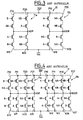
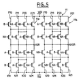
- the basic structure of a door OU-Exclusive made using CMOS technology easily deduced from the basic structure of an inverter produced using this technology (FIG. 1) on the one hand, and the truth table of the OU-Exclusive function (Figure 2) on the other hand.
Landscapes
- Physics & Mathematics (AREA)
- Engineering & Computer Science (AREA)
- Computer Hardware Design (AREA)
- Computing Systems (AREA)
- General Engineering & Computer Science (AREA)
- Mathematical Physics (AREA)
- Nonlinear Science (AREA)
- Logic Circuits (AREA)
Claims (3)
- Exklusiv-ODER-Gatter mit vier Eingänge, die jeweils paarweise komplementär sind (A und NA, und B und NB) und mit zwei komplementären Ausgängen (XOR und NXOR), in dem zwei Zellen (11a-11b) jeweils parallel geschaltet zwei Zweige (P10, P20) umfassen, die jeweils einen ersten und einen zweiten MOS-Transistor des P-Typs aufweisen, die zwischen einem oberen Versorgüngsanschluß und einem Ausgangsknoten (XOR oder NXOR) in Reihe geschaltet und durch einen Zwischenknoten getrennt sind, und auch jeweils zwei parallel geschaltete Zweige (N10, N20) umfassen, die jeweils einen ersten und einen zweiten MOS-Transistor des N-Typs aufweisen, welche zwischen dem Ausgangsknoten und einem unteren Versorgungsanschluß in Reihe geschaltet und durch einen Zwischenknoten getrennt sind;
wobei die Steuergates der zwei Transistoren jedes der vier Zweige jeder Zelle exklusiv eines der vier Eingangspaare empfangen ({A, B}, {NA, B}, {A, NB}oder {NA, NB});
wobei die beiden Zweige ein und derselben Zelle, welche Transistoren des gleichen Typs umfaßt, paarweise komplementäre Eingangspaare empfangen;
wobei die zwei Zweige einer bestimmten Zelle egal welchen Typs, sei es P oder N, jeweils die zwei gleichen Eingangspaare wie die zwei Zweige der anderen Zelle des anderen Typs, welche Transistoren umfaßt, sei es N oder P, empfangen;
dadurch gekennzeichnet, daß zu jedem Zweig (P10, P20, N10 und N20) femer ein Zweig des gleichen Typs, der Transistoren umfaßt und Gabelzweig (P11, P21, N11 bzw. N21) dieses Zweigs genannt wird, parallel geschaltet ist, wobei der erste und der zweite Transistor an ihrem Steuergate das Eingangspaar empfängt, das zu dem Eingangspaar an den Steuergates der Transistoren dieses Zweigs invers ist;
und daß in jeder Zelle der Zwischenknoten eines beliebigen Zweigs eines bestimmten Typs, der Transistoren umfaßt, sei es N oder P, mit einem Zwischenknoten des Gabelzweigs des anderen Zweigs desselben Typs, der Transistoren umfaßt, verbunden ist. - Exklusiv-ODER-Gatter nach Anspruch 1, dadurch gekennzeichnet, daß die Größe des Kanals der MOS-Transistoren des P-Typs 2,5 mal größer ist als die der MOS-Transistoren des N-Typs.
- Frequenzmultiplizierer mit einer Kette aus N Verzögerungsschaltkreisen zum Erzeugen von N zeitlich phasenverschobenen Abtastsignalen ausgehend von einem Taktsignal mit vorgegebener Frequenz fo, mit Mitteln zum Abtasten eines N-Bitwortes, das zu übertragende Information darstellt und sich mit Hilfe der N Abtastsignalen, welche N abgetastete Signale erzeugen, seriell darstellt, und einem Exklusiv-ODER-Gatterbaum mit vier paarweise komplementären Eingängen und zwei komplementären Ausgängen, die an ihren Eingängen die N abgetasteten Signale und deren logische Komplemente empfangen,
dadurch gekennzeichnet, daß die Exklusiv-ODER-Gatter des Baums Exklusiv-ODER-Gatter gemäß einem der Ansprüche 1 oder 2 sind.
Applications Claiming Priority (2)
| Application Number | Priority Date | Filing Date | Title |
|---|---|---|---|
| FR9711956 | 1997-09-25 | ||
| FR9711956A FR2768872B1 (fr) | 1997-09-25 | 1997-09-25 | Porte logique ou-exclusif a quatre entrees complementaires deux a deux et a deux sorties complementaires, et multiplieur de frequence l'incorporant |
Publications (2)
| Publication Number | Publication Date |
|---|---|
| EP0905907A1 EP0905907A1 (de) | 1999-03-31 |
| EP0905907B1 true EP0905907B1 (de) | 2003-05-14 |
Family
ID=9511484
Family Applications (1)
| Application Number | Title | Priority Date | Filing Date |
|---|---|---|---|
| EP98402263A Expired - Lifetime EP0905907B1 (de) | 1997-09-25 | 1998-09-14 | Exklusiv-Oder-Gatter mit vier zwei-zu-zwei komplementären Eingängen und zwei komplementären Ausgängen sowie Frequenzmultiplizierer damit |
Country Status (4)
| Country | Link |
|---|---|
| US (1) | US6137309A (de) |
| EP (1) | EP0905907B1 (de) |
| DE (1) | DE69814552D1 (de) |
| FR (1) | FR2768872B1 (de) |
Families Citing this family (11)
| Publication number | Priority date | Publication date | Assignee | Title |
|---|---|---|---|---|
| US6414519B1 (en) * | 2000-09-15 | 2002-07-02 | Applied Micro Circuits Corporation | Equal delay current-mode logic circuit |
| US6724221B2 (en) * | 2002-03-28 | 2004-04-20 | International Business Machines Corporation | Circuitry having exclusive-OR and latch function, and method therefor |
| US6566912B1 (en) * | 2002-04-30 | 2003-05-20 | Applied Micro Circuits Corporation | Integrated XOR/multiplexer for high speed phase detection |
| TWI281317B (en) * | 2005-03-07 | 2007-05-11 | Sunplus Technology Co Ltd | Self DC-bias high frequency logic gate, NAND gate, and NOR gate using the same |
| US7285986B2 (en) * | 2005-08-22 | 2007-10-23 | Micron Technology, Inc. | High speed, low power CMOS logic gate |
| US7242219B1 (en) * | 2005-09-08 | 2007-07-10 | Advanced Micro Devices, Inc. | Circuit for parity tree structure |
| US7725512B1 (en) * | 2006-04-26 | 2010-05-25 | Altera Corporation | Apparatus and method for performing multiple exclusive or operations using multiplication circuitry |
| US7557614B1 (en) * | 2008-07-15 | 2009-07-07 | International Business Machines Corporation | Topology for a n-way XOR/XNOR circuit |
| JP2013074560A (ja) | 2011-09-29 | 2013-04-22 | Elpida Memory Inc | 論理回路及びデータ処理システム |
| KR102276890B1 (ko) | 2014-08-14 | 2021-07-12 | 삼성전자주식회사 | 주파수 더블러 |
| US10756753B2 (en) * | 2018-10-25 | 2020-08-25 | Arm Limited | Data compressor logic circuit |
Family Cites Families (5)
| Publication number | Priority date | Publication date | Assignee | Title |
|---|---|---|---|---|
| JPS5765927A (en) * | 1980-10-13 | 1982-04-21 | Hitachi Ltd | Logical operation circuit |
| JPS61294934A (ja) * | 1985-06-21 | 1986-12-25 | Mitsubishi Electric Corp | 半導体装置およびデ−タ伝送路 |
| JPH05152936A (ja) * | 1991-11-29 | 1993-06-18 | Oki Electric Ind Co Ltd | 論理回路 |
| FR2714550B1 (fr) * | 1993-12-24 | 1996-02-02 | Bull Sa | Arbre de portes logiques OU-Exclusif et multiplieur de fréquence l'incorporant. |
| JPH0818437A (ja) * | 1994-01-25 | 1996-01-19 | Texas Instr Inc <Ti> | 立ち上り時間及び立ち下がり時間を一致させた論理ゲート及びその構築方法 |
-
1997
- 1997-09-25 FR FR9711956A patent/FR2768872B1/fr not_active Expired - Fee Related
-
1998
- 1998-09-14 EP EP98402263A patent/EP0905907B1/de not_active Expired - Lifetime
- 1998-09-14 DE DE69814552T patent/DE69814552D1/de not_active Expired - Lifetime
- 1998-09-23 US US09/159,316 patent/US6137309A/en not_active Expired - Lifetime
Also Published As
| Publication number | Publication date |
|---|---|
| FR2768872A1 (fr) | 1999-03-26 |
| EP0905907A1 (de) | 1999-03-31 |
| US6137309A (en) | 2000-10-24 |
| DE69814552D1 (de) | 2003-06-18 |
| FR2768872B1 (fr) | 2000-09-08 |
Similar Documents
| Publication | Publication Date | Title |
|---|---|---|
| EP0660525B1 (de) | Frequenzmultiplizierer mit einer Baumstruktur von CMOS logischen Gattern des Typs "Exclusiv-ODER" | |
| EP0905907A1 (de) | Exklusiv-Oder-Gatter mit vier zwei-zu-zwei komplementären Eingängen und zwei komplementären Ausgängen sowie Frequenzmultiplizierer damit | |
| EP1863179A1 (de) | Niveauverschiebungsschaltkreis | |
| FR2593652A1 (fr) | Reseau logique programmable a logique dynamique a horloge unique. | |
| FR2488006A1 (fr) | Circuit de report perfectionne pour un additionneur binaire | |
| EP0194195B1 (de) | Statische bistabile Kippschaltung in CMOS-Technologie | |
| EP0262032B1 (de) | Binärer Addierer mit festem Operand und paralleler/serieller Multiplikator mit solchen Addierern | |
| EP3376670B1 (de) | Konfigurierbare verzögerungsleitung | |
| EP0006053A1 (de) | Differenzbildungsvorrichtung mit Ladungskopplung; Filter und Verzögerungsleitung mit einer solchen Vorrichtung | |
| EP0309348B1 (de) | Binäre Additions- und Multiplikationsvorrichtung | |
| EP0283393A1 (de) | Binäre Rechnungseinrichtung | |
| EP0229433B1 (de) | Vorrichtung zum Prüfen eines kombinatorischen logischen Schaltkreises | |
| WO2007000387A1 (fr) | Commutateur de courant a paire differentielle de transistors alimente par une faible tension vcc | |
| EP0424222A1 (de) | Integrierte Logikschaltung mit einstellbaren Àbergangszeiten | |
| EP0065460B1 (de) | Parallelzähler in integrierter MOS-Schaltung und seine Anwendung in einem Binäraddierer | |
| EP1845619A1 (de) | Pufferkreis, der Mittel zur Steuerung der Steilheit des Ausgangssignals umfasst | |
| FR2573939A1 (fr) | Circuit multiplexeur de signaux integre a quatre voies d'entree | |
| EP0186533A1 (de) | Dynamisches Speicherelement und seine Verwendung in einer Master-Slave-Kippschaltung und in programmierbaren sequentiellen Schaltungen | |
| EP0687071A1 (de) | Vorrichtung mit einer aus dynamischen Logik-Stufen gebauten Schaltung | |
| EP1322076A1 (de) | Vermittlungsvorrichtung mit mitteln für lokale Dekodierung | |
| EP0239168A2 (de) | Arithmetisch-logische Schaltung | |
| EP1777904B1 (de) | Multiplexer mit hoher Bit-Rate mit paralleler Architektur | |
| EP0027884B1 (de) | Schaltungsanordnung mit mindestens zwei verschiedene Anstiegszeiten aufweisenden Halbleitervorrichtungen in MTL-Technologie und davon abgeleitete logische Schaltungen | |
| EP1320227A2 (de) | Schaltvorrichtung mit Referenzkanal auf gemeinsame Spannung | |
| EP0720173A1 (de) | Statischer Speicherbaustein des Flip-Flop-Registertyps |
Legal Events
| Date | Code | Title | Description |
|---|---|---|---|
| PUAI | Public reference made under article 153(3) epc to a published international application that has entered the european phase |
Free format text: ORIGINAL CODE: 0009012 |
|
| AK | Designated contracting states |
Kind code of ref document: A1 Designated state(s): DE FR GB IT |
|
| AX | Request for extension of the european patent |
Free format text: AL;LT;LV;MK;RO;SI |
|
| 17P | Request for examination filed |
Effective date: 19990518 |
|
| AKX | Designation fees paid |
Free format text: DE FR GB IT |
|
| RAP1 | Party data changed (applicant data changed or rights of an application transferred) |
Owner name: STMICROELECTRONICS S.A. |
|
| GRAH | Despatch of communication of intention to grant a patent |
Free format text: ORIGINAL CODE: EPIDOS IGRA |
|
| GRAH | Despatch of communication of intention to grant a patent |
Free format text: ORIGINAL CODE: EPIDOS IGRA |
|
| GRAA | (expected) grant |
Free format text: ORIGINAL CODE: 0009210 |
|
| AK | Designated contracting states |
Designated state(s): DE FR GB IT |
|
| PG25 | Lapsed in a contracting state [announced via postgrant information from national office to epo] |
Ref country code: IT Free format text: LAPSE BECAUSE OF FAILURE TO SUBMIT A TRANSLATION OF THE DESCRIPTION OR TO PAY THE FEE WITHIN THE PRESCRIBED TIME-LIMIT;WARNING: LAPSES OF ITALIAN PATENTS WITH EFFECTIVE DATE BEFORE 2007 MAY HAVE OCCURRED AT ANY TIME BEFORE 2007. THE CORRECT EFFECTIVE DATE MAY BE DIFFERENT FROM THE ONE RECORDED. Effective date: 20030514 |
|
| REG | Reference to a national code |
Ref country code: GB Ref legal event code: FG4D Free format text: NOT ENGLISH |
|
| RIN1 | Information on inventor provided before grant (corrected) |
Inventor name: COUTEAUX, PASCAL Inventor name: MARBOT, ROLAND |
|
| REF | Corresponds to: |
Ref document number: 69814552 Country of ref document: DE Date of ref document: 20030618 Kind code of ref document: P |
|
| GBT | Gb: translation of ep patent filed (gb section 77(6)(a)/1977) | ||
| PG25 | Lapsed in a contracting state [announced via postgrant information from national office to epo] |
Ref country code: DE Free format text: LAPSE BECAUSE OF FAILURE TO SUBMIT A TRANSLATION OF THE DESCRIPTION OR TO PAY THE FEE WITHIN THE PRESCRIBED TIME-LIMIT Effective date: 20030815 |
|
| PGFP | Annual fee paid to national office [announced via postgrant information from national office to epo] |
Ref country code: DE Payment date: 20030925 Year of fee payment: 6 |
|
| PLBE | No opposition filed within time limit |
Free format text: ORIGINAL CODE: 0009261 |
|
| STAA | Information on the status of an ep patent application or granted ep patent |
Free format text: STATUS: NO OPPOSITION FILED WITHIN TIME LIMIT |
|
| 26N | No opposition filed |
Effective date: 20040217 |
|
| PGFP | Annual fee paid to national office [announced via postgrant information from national office to epo] |
Ref country code: GB Payment date: 20060905 Year of fee payment: 9 |
|
| GBPC | Gb: european patent ceased through non-payment of renewal fee |
Effective date: 20070914 |
|
| REG | Reference to a national code |
Ref country code: FR Ref legal event code: ST Effective date: 20080531 |
|
| PG25 | Lapsed in a contracting state [announced via postgrant information from national office to epo] |
Ref country code: FR Free format text: LAPSE BECAUSE OF NON-PAYMENT OF DUE FEES Effective date: 20071001 |
|
| PGFP | Annual fee paid to national office [announced via postgrant information from national office to epo] |
Ref country code: FR Payment date: 20060928 Year of fee payment: 9 |
|
| PG25 | Lapsed in a contracting state [announced via postgrant information from national office to epo] |
Ref country code: GB Free format text: LAPSE BECAUSE OF NON-PAYMENT OF DUE FEES Effective date: 20070914 |