EP0224125A2 - Amplificateur de détection pour une mémoire non volatile - Google Patents
Amplificateur de détection pour une mémoire non volatile Download PDFInfo
- Publication number
- EP0224125A2 EP0224125A2 EP86115696A EP86115696A EP0224125A2 EP 0224125 A2 EP0224125 A2 EP 0224125A2 EP 86115696 A EP86115696 A EP 86115696A EP 86115696 A EP86115696 A EP 86115696A EP 0224125 A2 EP0224125 A2 EP 0224125A2
- Authority
- EP
- European Patent Office
- Prior art keywords
- current
- transistor
- conductivity
- memory cell
- logic state
- Prior art date
- Legal status (The legal status is an assumption and is not a legal conclusion. Google has not performed a legal analysis and makes no representation as to the accuracy of the status listed.)
- Granted
Links
- 230000015654 memory Effects 0.000 title claims abstract description 111
- 238000000034 method Methods 0.000 claims description 23
- 230000007704 transition Effects 0.000 claims description 15
- 230000004044 response Effects 0.000 claims description 13
- 230000008878 coupling Effects 0.000 claims description 4
- 238000010168 coupling process Methods 0.000 claims description 4
- 238000005859 coupling reaction Methods 0.000 claims description 4
- 230000008569 process Effects 0.000 description 12
- 238000010586 diagram Methods 0.000 description 4
- 230000000670 limiting effect Effects 0.000 description 3
- 238000013459 approach Methods 0.000 description 2
- 239000003990 capacitor Substances 0.000 description 2
- 230000001419 dependent effect Effects 0.000 description 2
- 230000007246 mechanism Effects 0.000 description 2
- 230000002829 reductive effect Effects 0.000 description 2
- 230000006399 behavior Effects 0.000 description 1
- 230000008859 change Effects 0.000 description 1
- 230000000295 complement effect Effects 0.000 description 1
- 238000001514 detection method Methods 0.000 description 1
- 238000007599 discharging Methods 0.000 description 1
- 230000000694 effects Effects 0.000 description 1
- 230000007613 environmental effect Effects 0.000 description 1
- 230000002401 inhibitory effect Effects 0.000 description 1
- 230000004048 modification Effects 0.000 description 1
- 238000012986 modification Methods 0.000 description 1
- 229910021420 polycrystalline silicon Inorganic materials 0.000 description 1
- 229920005591 polysilicon Polymers 0.000 description 1
- 238000011084 recovery Methods 0.000 description 1
- 230000003068 static effect Effects 0.000 description 1
- 239000000758 substrate Substances 0.000 description 1
Images
Classifications
-
- G—PHYSICS
- G11—INFORMATION STORAGE
- G11C—STATIC STORES
- G11C11/00—Digital stores characterised by the use of particular electric or magnetic storage elements; Storage elements therefor
- G11C11/21—Digital stores characterised by the use of particular electric or magnetic storage elements; Storage elements therefor using electric elements
- G11C11/34—Digital stores characterised by the use of particular electric or magnetic storage elements; Storage elements therefor using electric elements using semiconductor devices
- G11C11/40—Digital stores characterised by the use of particular electric or magnetic storage elements; Storage elements therefor using electric elements using semiconductor devices using transistors
-
- G—PHYSICS
- G11—INFORMATION STORAGE
- G11C—STATIC STORES
- G11C16/00—Erasable programmable read-only memories
- G11C16/02—Erasable programmable read-only memories electrically programmable
- G11C16/06—Auxiliary circuits, e.g. for writing into memory
- G11C16/26—Sensing or reading circuits; Data output circuits
- G11C16/28—Sensing or reading circuits; Data output circuits using differential sensing or reference cells, e.g. dummy cells
-
- G—PHYSICS
- G11—INFORMATION STORAGE
- G11C—STATIC STORES
- G11C7/00—Arrangements for writing information into, or reading information out from, a digital store
- G11C7/06—Sense amplifiers; Associated circuits, e.g. timing or triggering circuits
- G11C7/062—Differential amplifiers of non-latching type, e.g. comparators, long-tailed pairs
-
- G—PHYSICS
- G11—INFORMATION STORAGE
- G11C—STATIC STORES
- G11C7/00—Arrangements for writing information into, or reading information out from, a digital store
- G11C7/14—Dummy cell management; Sense reference voltage generators
Definitions
- the present invention relates to sense amplifiers, and more particularly, to techniques for sensing data stored in memory cells in a non-volatile memory.
- Non-volatile memories include memories which retain data even when the power supply is turned off.
- Typical memories in this category are various read only memories (ROMs), such as mask programmable ROMs, erasable programmable ROMs (EPROMs), and electrically erasable read only memories (EEPROMs).
- ROMs read only memories
- EPROMs erasable programmable ROMs
- EEPROMs electrically erasable read only memories
- These memories typically have memory cells which are either in a high conductivity or low conductivity state.
- EPROMs and EEPROMs the memory cells have either a relatively high threshold voltage or a relatively low threshold voltage which is used to obtain the high and low conductivity states.
- Another typical characteristic is that the memory cells have a single output which is connected to a bit line. Consequently, a number of sense amplifiers for ROMs were single-ended. More recently, however, it has been more common to use reference cells (also commonly called dummy cells) so that differential amplifying techniques could be
- RAMs random access memories
- DRAMs dynamic RAMs
- SRAMs static RAMs
- This approach uses the inherent current carrying aspect of non-volatile cells to generate a voltage differential which is then amplified by a voltage differential amplifier.
- This technique is still primarily a differential voltage amplifier technique.
- One problem is that there is a significant performance dependence on changes in process parameters.
- the bias point established on the differential voltage amplifier is dependent upon a ratio of conductivities of a P channel transistor and an N channel floating transistor.
- transistors of the same type track very well over process variations, transistors of different types do not. There is some tracking between regular N and P channel transistors and between regular N channel and N channel floating gate transistors. It is thus desirable that performance should be ratioless rather than depend upon the ratio of transistors of differing types.
- An object of the present invention is to provide an improved sensing technique for a non-volatile memory.
- Another object of the invention is to provide a non-volatile memory with improved insensitivity to process variations.
- Yet another object of the invention is to provide a data sensing system with improved insensitivity to process variations.
- a memory which has an array of non-volatile memory cells which are in either a programmed or unprogrammed state.
- the programmed state is characterized as having a first conductivity and the unprogrammed state is characterized as having a second conductivity.
- the memory comprises a decoder, a reference cell, a reference current circuit, a logic state current circuit, a first current mirror slave, a second current mirror slave, and an output circuit.
- the decoder selects a memory cell in response to an address and couples said selected memory cell to a common data line.
- the reference cell is unprogrammed and has the second conductivity.
- the reference current circuit establishes a reference current proportional to the second conductivity.
- the logic state current circuit establishes a logic state current related to the conductivity of the selected memory cell.
- the first current mirror slave establishes a reference current limit between a first power supply node and an output node as a predetermined proportion of the reference current.
- the second current mirror slave establishes a control current limit between a second power supply terminal and the output node as a predetermined proportion of the logic state current.
- the control current limit is of a first magnitude if the logic state current is related to the first conductivity and is of a second magnitude if the logic state current is related to the second conductivity.
- the output circuit provides an output signal at a first logic state when the second current mirror slave establishes the control current limit at the first magnitude, and provides the output signal at a second logic state when the second current mirror slave establishes the control current limit at the second magnitude.
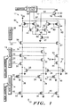
- FIG. l Shown in FIG. l is a memory l0 comprised generally of a sense amplifier ll, a memory array l2, a column decoder l3, a row decoder l4, an output buffer l6, a control clock l7, reference voltage generator l8, coupling transistors l9, 20, 2l, 22, 23, 24, 26, and 27, bit line precharge transistors 28, 29, 30, and a data line 3l.
- Transistors l9-24 and 26-30 are N channel transistors.
- Memory l0 has both N and P channel transistors for controlling array l2.
- the N channel transistors have a threshold voltage between 0.5 and 0.8 volt.
- the P channel transistors have a threshold voltage of between -0.5 and -0.8 volt.
- Array l2 is comprised of floating gate transistors which are either in a low or high threshold state.
- the floating gate transistors shown in FIG. l comprising array l2 are transistors 32, 33, 34, 35, 36, and 37; bit lines 38 39, and 40; and word lines 4l and 42.
- Floating gate transistors are EPROM cells which are erased to the low threshold voltage state by the application of ultra-violet light and are electrically programmed to the high threshold state. This is conventional for EPROM cells.
- Sense amplifier ll is comprised of N channel transistors 44, 45, 46 and 47 and P channel transistors 5l, 52, 53, and 54.
- Column decoder l3 provides a plurality of outputs for selecting which bit line will provide data to data line 3l.
- the outputs shown in FIG. l are signals Cl, C2, C3, and C4.
- Transistor l9 has a drain connected to data line 3l, a gate for receiving signal C2 from column decoder l3, and a source.
- Transistor 20 has a drain connected to the source of transistor l9, a gate for receiving signal C4 from column decoder l3, and a source connected to bit line 38.
- Transistor 2l has a drain connected to data line 3l, a gate for receiving a signal Cl from column decoder l3, and a source.
- Transistor 22 has a drain connected to the source of transistor 2l, a gate for receiving signal C3 from column decoder l3, and a source connected to bit line 39.
- bit line 38 is selected by the column address
- column decoder l3 drives signals C2 and C4 active at a logic high so that transistors l9 and 20 couple bit line 38 to data line 3l.
- bit line 39 is selected by the column address
- column decoder l3 drives signals Cl and C3 active at a logic high so that transistors 2l and 22 couple bit line 39 to data line 3l.
- Transistors 23 and 24 are used to simulate transistor coupling pairs l9-20 and 2l-22.
- Transistor 23 has a gate connected to a positive power supply terminal VDD for receiving a positive power supply voltage such as 5 volts, a drain, and a source.
- Transistor 24 has a drain connected to the source of transistor 23, a gate connected to VDD, and a drain connected to bit line 40.
- Reference voltage generator ls has an output which provides a reference voltage VR at about 2.l volts.
- Voltage VR is used to limit the voltage on a selected bit line such as one of bit lines 38 and 39.
- Voltage VR limits bit line voltage via data line 3l.
- the voltage is limited on data line 3l via transistor 26.
- Transistor 26 has a drain connected to a data input of sense amplifier ll, a gate for receiving voltage VR from reference voltage generator l8, and a source connected to data line 3l.
- the voltage on data line l3 is thus limited to voltage VR of about 2.l volts minus the threshold voltage of transistor 26. This threshold voltage including body effect, which is well known in the art, will be nominally 0.9 volt.
- Transistor 27 is used to match the affect of transistor 26.
- Transistor 27 has a drain connected to a reference input of sense amplifier ll, a gate for receiving voltage VR from generator l8, and a source connected to the drain of transistor 23.
- Transistor 27 limits the voltage on the drain of transistor 23 in the same way that transistor 26 limits the voltage on data line 3l.
- bit line 40 is limited in voltage in the same way as a selected bit line is limited in voltage.
- Transistors 28-30 are used to precharge bit lines 38-40 to a voltage near ground potential in response to a bit line precharge signal BP generated by control clock l7.
- Transistors 28, 29, and 30 each have a gate for receiving signal BP from clock l7, a source connected to ground, and a drain. The drains of transistors 28, 29, and 30 are connected to bit lines 38, 39, and 40, respectively.
- clock l7 drives signal BP active to a logic high
- transistors 28-30 precharge bit lines 38-40 by discharging bit lines 38-40 well below the voltage to which bit lines 38-40 are limited by voltage VR and transistors 26 and 27.
- Transistors 32-37 are programmed to either a high threshold voltage or a low threshold voltage.
- the low threshold state is the erased state obtained after exposure to ultra-violet light.
- Programming of array l2 is achieved by selectively raising the threshold voltage of the floating gate transistors which comprise array l2 such as transistors 32-35.
- Transistors 36 and 37 are used as references and are in the erased state only.
- Transistor 32 has a drain connected to bit line 38, a gate connected to word line 4l, and a source connected to ground.
- Transistor 33 has a drain connected to bit line 38, a gate connected to word line 42, and a source connected to ground.
- Transistor 34 has a drain connected to bit line 39, a gate connected to word line 4l, and a source connected to ground.
- Transistor 35 has a drain connected to bit line 39, a gate connected to word line 42, and a source connected to ground.
- Transistor 36 has a drain connected to bit line 40, a gate connected to word line 4l, and a source connected to ground.
- Transistor 37 has a drain connected to bit line 40, a gate connected to word line 42, and a source connected to ground.
- Row decoder l4 has a plurality of row decoder output signals for enabling a word line as selected by a row address received by row decoder l4.
- row decoder l4 In response to the row address, row decoder l4 causes one of these row decoder output signals to become active. This type of row decoder is well known in the art. Row decoder output signals Rl and R2 are shown as being outputs of row decoder l4. Row decoder l4 outputs signal Rl onto word line 4l and signal R2 onto word line 42. A word line is enabled when the row decoder output signal corresponding thereto is active at a logic high. Word line 4l is enabled when row decoder l4 provides signal Rl at a logic high. Word line 42 is enabled when row decoder l4 provides signal R2 at a logic high.
- transistors 32, 34, and 36 are activated in accordance with the threshold voltage to which they are programmed. It is desirable that the high threshold voltage be above VDD so that the memory cell transistor having been programmed to the high voltage state will be completely non-conductive when the word line to which it is connected is enabled.
- the low voltage state is desirably well below the voltage of an enabled word line so that a memory cell transistor having the low voltage state will be highly conductive when the word line to which it is connected is enabled.
- the high threshold voltage may not exceed VDD.
- a memory cell transistor which is programmed to the high voltage state may in fact be conductive when the word line is enabled.
- the high and low threshold voltage states must then be distinguished on the basis of relative degree of conductivity rather than simply distinguishing between memory cells which are conductive or non-conductive.
- Bit line 40 and and the memory cells connected thereto are used as a reference for emulating an unprogrammed cell.
- Sense amplifier ll compares the conductivity of its reference input to that of its data input to determine if the selected memory cell which is coupled to the data input is in the low or high threshold state.
- Sense amplifier ll provides a sense amplifier output signal SO at a logic high when the selected memory cell is in the low threshold state which is the relatively higher conductivity state.
- Buffer l6 has an input for receiving signal SO and an output for providing data output signal DO.
- Buffer l6 receives a chip enable signal CE and a buffer enable signal BE.
- the chip enable signal CE is derived from an externally generated signal *CE which enables memory l0 at a logic low and disables memory l0 at a logic high. This operation of memory l0 in response to signal *CE is conventional.
- Signal CE is complementary to signal *CE.
- Amplifier l6 is enabled when signal CE is a logic high and disable when signal CE is a logic low. Buffer l6 is clocked by a buffer enable signal BE received from clock l7.
- buffer l6 When signal BE is active, buffer l6 provides signal DO responsive to the logic state of signal SO. When signal BE is inactive, buffer l6 is inactive and provides signal DO as a high impedance. A buffer with this high impedance feature is commonly known as a tri-state buffer.
- Clock l7 includes a timing feature so that signal BE is provided in the active state just when sense amplifier ll provides signal SO as a valid indication of the program state of the selected memory cell. Buffer l6 has a comparatively large drive capability which causes it to draw significant current when it changes state. Signal BE is used to hold buffer l6 in a predetermined state, tri-stated, until signal SO is indicative of the logic state of the accessed memory cell. This prevents any portion of the actual sensing operation from being disturbed by switching transients or by noise coupled into array l2 which occurs when buffer l6 switches logic states.
- Transistor 5l has a drain and a gate, which act as the data input of sense amplifier ll, connected to the drain of transistor 26, and a source connected to VDD.
- Transistor 54 has a drain and a gate, which act as the reference input of sense amplifier ll, connected to the drain of transistor 27, and a source connected to VDD.
- Transistor 52 has a source connected to VDD, a gate connected to the drain and gate of transistor 5l, and a drain as the output of sense amplifier ll.
- Transistor 44 has a drain connected to the drain of transistor 52, a gate for receiving a sense amplifier reset signal SR from clock l7, and a source connected to a node 56.
- Sense amplifier ll is reset by signal SR becoming active at a logic high which causes signal SO to be a logic low.
- Node 56 is clamped to ground by transistor 47 during the operation of sense amplifier ll.
- Transistor 47 has a drain connected to node 56, a gate for receiving a chip enable signal CE.
- Sense amplifier ll is enabled by chip enable signal CE being active.
- signal CE is a signal provided externally to memory l0.
- signal CE When signal CE is active, it indicates that memory is to respond to the addresses it receives to either perform a read or a write. Thus, for operational purposes, node 56 can be viewed as ground.
- Transistor 45 has a drain connected to the drain of transistor 52, a source connected to node 56, and a gate.
- Transistor 46 has a source connected to node 56, a drain and a gate connected to the gate of transistor 45.
- Transistor 53 has a drain connected to the gate and drain of transistor 46, a source connected to VDD, and a gate connected to the gate and drain of transistor 54.
- Sense amplifier ll is initialized for a new sensing operation when signal SR becomes active which resets signal SO to a logic low.
- Signal SR is active as logic high pulse of 45-85 nanoseconds (ns) in duration. This duration of signal SR at a logic high varies with process variations.
- Signal SR becomes active in response to an address transition or in response to signal CE becoming inactive.
- signal BP is also activated as a logic high pulse of about l0 ns. duration. This precharges the bit lines including bit line 38 below the voltage limit of about l.2 volt supplied by signal VR via transistor 26.
- transistor 32 is the newly selected memory cell which is selected by row decoder l4 selecting word line 4l and column decoder l3 selecting bit line 38.
- Word line 4l is enabled and bit line 38 is coupled to data line 3l.
- Transistors 32 and 36 accordingly receive logic high inputs on their gates. Also assume that transistor 32 is in the erased or low threshold state which is the relatively high conductivity state. Transistor 36, as a reference cell, is also in the low threshold state. All of the transistors in array l2 are closely matched. Consequently, transistors 32 and 36 have very nearly the same conductivity.
- Transistor 54 similarly supplies current to bit line 40.
- the current supplied via transistor 54 to bit line 40 is determined by the conductivity of transistor 36 and the voltage limiting affect of signal VR.
- bit lines 38 and 40 at the same voltage and transistors 32 and 36 having the same conductivity, the currents through transistors 5l and 54 are the same.
- Transistors 5l and 54 are both forced into the saturation region of operation due to the gate to drain connection.
- the saturation region of operation is characterized as being that region of operation in which the current through the transistor is limited by the gate to source voltage and can increase only slightly with increases in the magnitude of the drain to source voltage.
- Transistors 52 and 53 form current mirrors with transistors 5l and 54.
- Transistors 5l and 52 form a current mirror 6l in which transistor 5l is the master and transistor 52 is the slave.
- Transistors 53 and 54 form a current mirror 62 in which transistor 54 is the master and transistor 53 is the slave.
- the gains and thresholds of transistors 53 and 54 are matched to be the same.
- the actual values of the gains and thresholds of transistors are difficult to keep constant over process variations which are likely to occur.
- the relative gains and thresholds of the same transistor types are quite constant with process variations if care is taken in the layout of the transistors.
- the capability of maintaining relative gains and thresholds is known in the art. Consequently, the gains and thresholds of transistors 53 and 54 can be relied upon to be the same.
- transistor 54 The current flowing through transistor 54 is thus reflected to transistor 53 in a one to one ratio.
- the master In a current mirror configuration the master is forced into the saturation region, and the slave has the same gate to source voltage as the master so that the current flowing through the slave will be a proportion of the current flowing through the master as determined by the gain ratios of the master and the slave so long as there is not some mechanism operating to limit the current below that established by the gain ratios.
- Transistors 46 and 47 are in series with transistor 53 but are of sufficient gain to not cause current limiting through transistor 53. The current through transistor 53 is very close to the current flowing through transistor 54.
- Transistor 46 has the same current as transistor 53 and therefore the same as transistor 54.
- Transistors 45 and 46 form a current mirror 63 in which transistor 46 is the master and transistor 45 is the slave. Transistor 45 is chosen to have the same gain as transistor 46 so that transistor 45 is limited to carrying no more than the current flowing through transistor 54.
- Transistor 52 is chosen to have a gain twice that of transistor 5l so that the current carrying capability of transistor 52 is twice that of the current flowing through transistor 5l.
- a convenient technique to obtain double gain is to fabricate two identical transistors in parallel. This also is convenient for obtaining a matching threshold voltage.
- the current flowing through transistors 5l and 52 is virtually the same. This results in transistor 52 having twice the current carrying capability of transistor 45. In such case transistor 45 is in the saturation region, but transistor 52 is in the triode region.
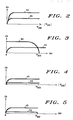
- Shown in FIG. 2 is the drain current versus the magnitude of the drain to source voltage (VDS) curves for transistors 52 and 45 for this described situation in which the current carrying capability of transistor 52 is twice that of transistor 45.
- VDS drain to source voltage
- FIG. 3 shows the same information as FIG. 2 except that instead of drain current being plotted against the magnitude of VDS, drain current is plotted against drain to source voltage as represented by the voltage of signal SO.
- the intersection of the curves is the voltage at which signal SO will be as a result of transistor 52 having twice the current carrying capability of transistor 45.
- the resulting voltage of signal SO is very near VDD as shown in FIG. 3. Buffer l6 thus easily recognizes signal SO as a logic high for the case in which a selected memory cell is in the low threshold state.
- the conductivity of the selected memory cell is much less than the selected reference cell, reference cell 36 in the present example.
- the current through transistor 32 as the selected memory cell is determined by the voltage on bit line 38 and the the conductivity of transistor 32. With the conductivity substantially reduced for the high threshold state and the bit line voltage the same, the current is substantially reduced in comparison to the low threshold voltage state.
- the conductivity of transistor 32 will be at least l0 times less for the high threshold voltage state than for the low threshold voltage state.
- Sense amplifier ll is effective even if the conductivity ratio of low threshold voltage to high threshold voltage is much less than l0.
- transistor 45 is twice that of transistor 52.
- FIG. 4 Shown in FIG. 4 are the drain current versus the magnitude of the drain to source voltage curves for this condition in which the current carrying capability of transistor 45 is twice that of transistor 52.
- the same information is shown in FIG. 5 except that instead of the magnitude of the drain to source voltage being plotted versus drain current, the voltage of signal SO is plotted versus drain current.
- the intersection of the two curves in FIG. 5 is the resulting voltage of signal SO.
- the resulting voltage of signal SO is very near zero or ground potential. This voltage is easily recognizable by buffer l6 as a logic low for the case in which the selected memory cell is programmed to the high threshold voltage state.
- transistor 52 When the current carrying capability of transistor 52 is twice as great as that of transistor 45, sense amplifier ll provides signal SO at a voltage easily recognizable as a logic high. When the current carrying capability of transistor 45 is twice as great as that of transistor 52, sense amplifier ll provides signal SO at a voltage easily recognizable as a logic low.
- Transistors 54, 53, and 46 act to limit the current carrying capability of transistor 45 in relation to the conductance of a selected reference memory cell.
- Transistor 5l acts to limit the current carrying capability of transistor 52 in relation to the conductance of the selected memory cell.
- Transistor 54 establishes a reference current therethrough which is related to the conductivity of a reference cell. Transistors 46, 53, and 54 cause transistor 45 to be current limited to the reference current.
- Transistor 5l establishes a current therethrough representative of the logic state of a selected memory cell.
- the current through transistor 5l causes the current carrying capability of transistor 52 to be significantly greater than the current carrying capability of transistor 45.
- the current through transistor 5l causes the current carrying capability of transistor 52 to be significantly less than the current carrying capability of transistor 45.
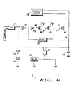
- Control clock l7 comprises an address transition detector (ATD) 7l, inverters 72 and 73, amplifiers 74 and 75, a word line 76, a floating gate transistor 77, a current source 78, a bit line 79, a reset circuit 80, a NAND gate 8l, and a delay circuit 82.
- ATD 7l In response to a change in a column or row address transition, ATD 7l generates a signal *PC as a logic low pulse of about l0 ns duration.
- the asterisk (*) in front of a signal is used to indicate that the signal is active at a logic low.
- Inverters 72 and 73 each have an input for receiving signal PC, and each have an output.
- Amplifier 75 has an input coupled to the output of inverter 72, and an output connected to word line 76.
- Amplifier 75 along with inverter 72 comprise the same circuit as used by row decoder l4 for enabling the word line.
- Word line 76 is made the same way as a word line, such as word line 4l, in array l2.
- Floating gate transistor 77 is an unprogrammed floating gate transistor which has a gate connected to word line 76, a drain connected to current source 78, and a source connected to ground. Transistor 77 is connected at the end of word line 76.
- Word line 76 has a plurality of floating gate transistors connected thereto such as transistors 83 and 84. The total number of floating gate transistors connected thereto is the same as for a word line in array l2 of FIG. l.
- inverter 72 When signal *PC is a logic low the output of inverter 72 is a logic high which activates reset circuit 80 which is connected to the output of inverter 72. When activated, reset circuit 80 resets word line 76 and bit line 79 to ground. Also when signal *PC is a logic low, inverter 73 provides a logic high output to an input of amplifier 74. Amplifier 74 has an input connected to the output of inverter 73, and an output for providing bit line precharge signal BP. Upon receiving the logic high from inverter 73, amplifier 74 switches signal BP from a logic low to a logic high. This causes the bit lines of array l2 to be precharged near ground.
- inverter 72 When signal *PC switches back to a logic high, inverter 72 provides a logic low output which deactivates reset circuit 80 and causes inverter 75 to provide a logic high onto word line 76 analogously to row decoder l4 enabling a word line.
- Word line 76 and the transistors connected thereto such as transistors 83 and 84 simulates the delay in enabling a word line in array l2.
- the delay in enabling a word line in array l2 will vary with process variations such as polysilicon conductivity, and word line width and depth. These variations are matched with word line 76 so as to match changes in word line delay.
- Transistor 77 receives the logic high and in response begins drawing current from current mirror 78.
- the delay is the summation of the duration of the logic low of pulse *PC, the delay of inverter 72 and inverter 75, and the propagation delay along word line 76.
- the delay from an address transition to enabling transistor 77 is the same as from an address transition to row decoder l4 enabling a memory cell at the end of a word line. This is ensured because the circuitry used for the delay in enabling transistor 77 is copied from the circuitry used for enabling a memory cell at the end of a word line.
- Floating gate transistor 77 draws a reference current from current mirror 78 which current mirror 78 uses to provide to bit line 79. Because transistor 77 is a floating gate transistor, it draws current analogous to that drawn by a memory cell. Additionally, transistor 77 matches the threshold voltage of a floating gate transistor in the unprogrammed state such as the reference transistors 36 and 37. Consequently, control block l7 includes tracking of threshold voltage variation over process variations as well as environmental variations.
- Current mirror 78 uses the current drawn through transistor 77 to determine the current supplied to bit line 79 to charge bit line 79 to a voltage which is detected by NAND gate 8l.
- NAND gate 8l has a first input connected to the end of bit line 79, a second input for receiving signal *PC, and an output for providing signal SR.
- Delay circuit 82 has an input for receiving signal SR, and an output for providing signal BE.
- Bit line 79 is made to have analogous capacitance characteristics to a bit line, such as bit line 38, in array l2.
- Each bit line 38 in array l2 has connected thereto the drain of floating gate transistors equal in number to the number of word lines. These drains add appreciably to the capacitance of bit line 38. This drain capacitance varies with process. Additionally, this drain capacitance has a unique relationship with voltage.
- bit line 79 has additional capacitance added thereto which is of the same type as that of floating gate transistor drains.
- the floating gate drains are N+ regions formed in the substrate in which memory l0 is formed.
- N+ regions comparable to those of floating gate drains are connected to bit line 79 to form the desired added capacitance.
- This added capacitance is indicated by a capacitor 90 connected between bit line 79 and ground in FIG. 6.
- Capacitor 90 thus has comparable characteristics to that of the drain capacitance on bit line 39. Consequently, variations in delay due to variations in drain capacitance on bit line line 39 will cause a similar variation in delay on bit line 79.
- NAND gate 8l When bit line 79 reaches sufficient voltage to be recognized as a logic high, NAND gate 8l will output signal SR as a logic low so long as the output of inverter 72 is a logic low.
- the output of inverter 72 is a logic low except in response to an address transition which causes signal *PC to pulse to a logic low.
- NAND gate 8l While signal *PC is a logic low, NAND gate 8l outputs signal SR at logic high and reset circuit 80 resets bit line 79 and word line 76.
- bit line 79 Prior to signal *PC switching to a logic low, bit line 79 will normally be a logic high so that NAND gate is supplying signal SR at logic low.
- signal SR is switched to a logic high and held there for the duration of signal *PC being a logic low. By the time signal *PC has switched back to a logic high, reset circuit 80 has reset bit line 79 to a logic low.
- Bit line 79 then causes NAND gate 8l to provide signal SR at a logic high until bit line 79 is charged to a logic high by word line 76 being enabled, transistor 77 drawing current from current mirror 78, and current mirror 78 supplying current to bit line 79 to provide the charging current which causes bit line 79 to reach a logic high.
- Signal SR is thus a logic high from the time an address transition is detected until bit line 79 is charged to a logic high. This time duration from signal *PC switching to a logic low until bit line 79 is charged to a logic high for the time duration of signal SR being a logic high is selected for optimum performance of sense amplifier ll.
- the elements selected for determining the logic high duration of signal SR were selected to match variations in memory l0 which affected the speed with which data could be sensed.
- the bit line variations, the word line variations, and threshold voltage variations of the unprogrammed memory cells have corresponding variations inherently present in control block l7 which determines the duration of signal SR at a logic high.
- Signal SR is used to hold the drains of transistors 52 and 45 at ground via transistor 44 until the selected bit line is actually ready to be read.
- the selected bit line is not ready to be read until the bit line has been charged because transistor 5l supplies the current which charges the selected bit line.
- the detection mechanism is dependent upon there being relatively little current flowing through transistor 5l.
- the current through transistor 5l is not significantly smaller than that through transistor 54 so that signal SO would move to a logic high during the charging of the selected bit line if transistor 44 did not hold it to ground.
- Signal SO switching to a logic high during the charging of the selected bit line would occur even if the selected memory cell is in the high threshold voltage state.
- Signal SR is supposed to be a logic low when the selected memory cell is in the high threshold state. If transistor 44 did not hold signal SO to a logic low during the charging of the selected bit line, then there would be a recovery time for signal SO to switch back to a logic low for the case of a selected high threshold voltage memory cell. Of course when the selected memory cell is in the low threshold voltage state, there is a transition time for signal SO to switch from a logic low to a logic high. This transition time is less than there would be for a logic high to logic low transition because transistor 52 has twice the current carrying capability of transistor 45 so that the capacitance at the drains of transistors 45 and 52 is quickly charged. The selected memory cell, even if in high threshold state, may have some leakage current which would be mirrored in transistor 52 and would then work against a logic high to logic low transition of signal SO.
- the timing of signal SR is thus very critical because it must be at a logic high long enough to avoid the potential false transition of signal SO while not being a logic high so long as to prevent sense amplifier ll from performing a sensing operation as soon as the selected bit line is ready. Consequently, great care is taken to ensure that signal SR occurs just as the selected bit line is charged.
- This is achieved by using the same type circuit elements for control clock l7 as is used in memory l0 in accessing a selected memory cell. By matching the circuit elements, the timing provided by clock l7 varies over process variations in the same way as the other circuitry of memory l0 which controls access time.
- clock l7 will also be faster so that signal SR is still provided just as a selected bit line is ready to be read.
- Clock l7 models the worst case access time which is for a selected memory cell which is at the end of a word line. Because the access time specification is for the worst case condition, there is no harm in inhibiting the access time for the faster locations to match the worst case location.
Landscapes
- Engineering & Computer Science (AREA)
- Microelectronics & Electronic Packaging (AREA)
- Computer Hardware Design (AREA)
- Read Only Memory (AREA)
Applications Claiming Priority (2)
| Application Number | Priority Date | Filing Date | Title |
|---|---|---|---|
| US801363 | 1985-11-25 | ||
| US06/801,363 US4713797A (en) | 1985-11-25 | 1985-11-25 | Current mirror sense amplifier for a non-volatile memory |
Publications (3)
| Publication Number | Publication Date |
|---|---|
| EP0224125A2 true EP0224125A2 (fr) | 1987-06-03 |
| EP0224125A3 EP0224125A3 (en) | 1989-10-11 |
| EP0224125B1 EP0224125B1 (fr) | 1993-07-14 |
Family
ID=25180904
Family Applications (1)
| Application Number | Title | Priority Date | Filing Date |
|---|---|---|---|
| EP86115696A Expired - Lifetime EP0224125B1 (fr) | 1985-11-25 | 1986-11-12 | Amplificateur de détection pour une mémoire non volatile |
Country Status (6)
| Country | Link |
|---|---|
| US (1) | US4713797A (fr) |
| EP (1) | EP0224125B1 (fr) |
| JP (1) | JPH0750557B2 (fr) |
| KR (1) | KR930008640B1 (fr) |
| DE (1) | DE3688696T2 (fr) |
| HK (1) | HK183595A (fr) |
Cited By (11)
| Publication number | Priority date | Publication date | Assignee | Title |
|---|---|---|---|---|
| EP0320779A3 (en) * | 1987-12-16 | 1990-03-21 | Kabushiki Kaisha Toshiba | Sense amplifier |
| EP0397355A3 (fr) * | 1989-05-09 | 1991-01-30 | Advanced Micro Devices, Inc. | Amplificateur de détection de courant |
| EP0347909A3 (fr) * | 1988-06-24 | 1991-08-14 | Kabushiki Kaisha Toshiba | Dispositif de mémoire permanente à l'opération stable dans une bande large de niveau de tension de la source de puissance |
| EP0396263A3 (fr) * | 1989-04-26 | 1991-12-27 | Exar Corporation | Dispositif EEPROM |
| EP0332135A3 (fr) * | 1988-03-09 | 1992-03-18 | Kabushiki Kaisha Toshiba | Circuit de mémoire non volatile ayant une faible consommation de courant et une plage de tension de fonctionnement étendue |
| EP0449311A3 (en) * | 1990-03-30 | 1992-08-05 | Fujitsu Limited | Signal amplifier circuit and semiconductor memory device using the same |
| EP0443776A3 (en) * | 1990-02-19 | 1992-11-04 | Fujitsu Limited | Sense circuit for non-volatile memory device |
| EP0484298A3 (en) * | 1990-10-31 | 1993-02-24 | Sgs-Thomson Microelectronics S.P.A. | Flash-eprom with enhanced immunity from soft-programming of reference cells |
| EP0405220A3 (fr) * | 1989-06-12 | 1994-02-23 | Toshiba Kk | |
| GB2299694A (en) * | 1995-04-07 | 1996-10-09 | Hyundai Electronics Ind | Method and apparatus for reading/writing data from/into semiconductor memory device |
| GB2321736A (en) * | 1997-01-30 | 1998-08-05 | Motorola Ltd | Sense amplifier for a memory |
Families Citing this family (41)
| Publication number | Priority date | Publication date | Assignee | Title |
|---|---|---|---|---|
| JPS62167698A (ja) * | 1986-01-20 | 1987-07-24 | Fujitsu Ltd | 半導体記億装置 |
| JPS62214597A (ja) * | 1986-03-17 | 1987-09-21 | Fujitsu Ltd | 不揮発性メモリ回路 |
| US4888503A (en) * | 1987-10-13 | 1989-12-19 | Intel Corporation | Constant current biased common gate differential sense amplifier |
| US5226013A (en) * | 1987-12-01 | 1993-07-06 | Sgs-Thomson Microelectronics S.R.L. | Bias and precharging circuit for use in reading EPROM cells |
| JPH07120720B2 (ja) * | 1987-12-17 | 1995-12-20 | 三菱電機株式会社 | 不揮発性半導体記憶装置 |
| US4785259A (en) * | 1988-02-01 | 1988-11-15 | Motorola, Inc. | BIMOS memory sense amplifier system |
| JPH02103797A (ja) * | 1988-10-12 | 1990-04-16 | Hitachi Ltd | センスアンプ回路 |
| JP2573335B2 (ja) * | 1988-11-09 | 1997-01-22 | 株式会社東芝 | 不揮発性メモリ |
| GB2232798B (en) * | 1989-06-12 | 1994-02-23 | Intel Corp | Electrically programmable read-only memory |
| US5198997A (en) * | 1989-08-11 | 1993-03-30 | Sony Corporation | Ultraviolet erasable nonvolatile memory with current mirror circuit type sense amplifier |
| FR2652672B1 (fr) * | 1989-10-02 | 1991-12-20 | Sgs Thomson Microelectronics | Memoire a temps de lecture ameliore. |
| IT1246241B (it) * | 1990-02-23 | 1994-11-17 | Sgs Thomson Microelectronics | Circuito per la lettura dell'informazione contenuta in celle di memoria non volatili |
| JPH04356799A (ja) * | 1990-08-29 | 1992-12-10 | Mitsubishi Electric Corp | 半導体記憶装置 |
| JP2673395B2 (ja) * | 1990-08-29 | 1997-11-05 | 三菱電機株式会社 | 半導体記憶装置およびそのテスト方法 |
| DE69026946T2 (de) * | 1990-11-19 | 1996-09-05 | Sgs Thomson Microelectronics | Verbesserte Abfühlschaltung für Speicheranordnungen wie nichtflüchtige Speicher mit kompensiertem Offsetstrom |
| JPH04195900A (ja) * | 1990-11-27 | 1992-07-15 | Nec Ic Microcomput Syst Ltd | カレントミラー型センスアンプ |
| JPH0636570A (ja) * | 1992-07-16 | 1994-02-10 | Mitsubishi Electric Corp | 半導体記憶装置のセンスアンプ回路 |
| US5608676A (en) * | 1993-08-31 | 1997-03-04 | Crystal Semiconductor Corporation | Current limited current reference for non-volatile memory sensing |
| DE69325810T2 (de) * | 1993-11-30 | 1999-11-18 | Stmicroelectronics S.R.L., Agrate Brianza | CMOS-integrierter Hochleistungs-Transkonduktanz-Operationsverstärker |
| JPH07211081A (ja) * | 1994-01-06 | 1995-08-11 | Mitsubishi Electric Corp | 半導体記憶装置 |
| US6353554B1 (en) | 1995-02-27 | 2002-03-05 | Btg International Inc. | Memory apparatus including programmable non-volatile multi-bit memory cell, and apparatus and method for demarcating memory states of the cell |
| US5638322A (en) * | 1995-07-19 | 1997-06-10 | Cypress Semiconductor Corp. | Apparatus and method for improving common mode noise rejection in pseudo-differential sense amplifiers |
| JPH09265791A (ja) * | 1996-03-28 | 1997-10-07 | Nec Corp | 半導体記憶装置 |
| US5729493A (en) * | 1996-08-23 | 1998-03-17 | Motorola Inc. | Memory suitable for operation at low power supply voltages and sense amplifier therefor |
| US5812456A (en) * | 1996-10-01 | 1998-09-22 | Microchip Technology Incorporated | Switched ground read for EPROM memory array |
| DE69905699T2 (de) | 1999-06-21 | 2003-10-16 | Stmicroelectronics S.R.L., Agrate Brianza | Lesevorgang für nichtflüchtige Speicher mit einem mit der Lesespannung variablen Abtaststrom, und Anordnung zur Verwirkligung dieses Vorgangs |
| US6573772B1 (en) | 2000-06-30 | 2003-06-03 | Intel Corporation | Method and apparatus for locking self-timed pulsed clock |
| JP2002251890A (ja) | 2001-02-26 | 2002-09-06 | Mitsubishi Electric Corp | 信号増幅回路およびそれを備える半導体記憶装置 |
| TW516267B (en) | 2002-01-16 | 2003-01-01 | Winbond Electronics Corp | Dynamic pre-charging current sensing amplifier |
| US6711068B2 (en) | 2002-06-28 | 2004-03-23 | Motorola, Inc. | Balanced load memory and method of operation |
| US6580298B1 (en) | 2002-06-28 | 2003-06-17 | Motorola, Inc. | Three input sense amplifier and method of operation |
| US6621729B1 (en) | 2002-06-28 | 2003-09-16 | Motorola, Inc. | Sense amplifier incorporating a symmetric midpoint reference |
| US6711052B2 (en) * | 2002-06-28 | 2004-03-23 | Motorola, Inc. | Memory having a precharge circuit and method therefor |
| JP4422558B2 (ja) * | 2004-06-10 | 2010-02-24 | 富士通マイクロエレクトロニクス株式会社 | メモリ装置 |
| US7522463B2 (en) | 2007-01-12 | 2009-04-21 | Atmel Corporation | Sense amplifier with stages to reduce capacitance mismatch in current mirror load |
| US7800968B2 (en) * | 2007-05-02 | 2010-09-21 | Infineon Technologies Ag | Symmetric differential current sense amplifier |
| US7782678B2 (en) | 2007-08-27 | 2010-08-24 | Infineon Technologies Ag | Self-timed integrating differential current sense amplifier |
| US8254178B2 (en) * | 2007-08-27 | 2012-08-28 | Infineon Technologies Ag | Self-timed integrating differential current |
| US8645617B2 (en) * | 2008-12-09 | 2014-02-04 | Rambus Inc. | Memory device for concurrent and pipelined memory operations |
| CN103794252B (zh) | 2012-10-29 | 2018-01-09 | 硅存储技术公司 | 用于读出放大器的低电压电流参考产生器 |
| US9659606B2 (en) * | 2014-12-17 | 2017-05-23 | Mediatek Inc. | Differential sensing circuit with dynamic voltage reference for single-ended bit line memory |
Family Cites Families (10)
| Publication number | Priority date | Publication date | Assignee | Title |
|---|---|---|---|---|
| US3936731A (en) * | 1974-11-14 | 1976-02-03 | Rca Corporation | Amplifier with fast recovery after input signal overswing |
| US4301518A (en) * | 1979-11-01 | 1981-11-17 | Texas Instruments Incorporated | Differential sensing of single ended memory array |
| JPS5693363A (en) * | 1979-12-04 | 1981-07-28 | Fujitsu Ltd | Semiconductor memory |
| JPS57198594A (en) * | 1981-06-01 | 1982-12-06 | Hitachi Ltd | Semiconductor storage device |
| JPS59186188A (ja) * | 1983-04-07 | 1984-10-22 | Fujitsu Ltd | センス増幅器 |
| JPS59218696A (ja) * | 1983-05-26 | 1984-12-08 | Toshiba Corp | 半導体メモリ |
| JPS6052996A (ja) * | 1983-09-02 | 1985-03-26 | Agency Of Ind Science & Technol | センスアンプ回路 |
| JPH0666115B2 (ja) * | 1983-09-26 | 1994-08-24 | 株式会社東芝 | 半導体記憶装置 |
| JPS6070591A (ja) * | 1983-09-28 | 1985-04-22 | Nec Corp | センスアンプ |
| JPS6080196A (ja) * | 1983-10-07 | 1985-05-08 | Mitsubishi Electric Corp | 半導体記憶装置 |
-
1985
- 1985-11-25 US US06/801,363 patent/US4713797A/en not_active Expired - Fee Related
-
1986
- 1986-11-12 EP EP86115696A patent/EP0224125B1/fr not_active Expired - Lifetime
- 1986-11-12 DE DE86115696T patent/DE3688696T2/de not_active Expired - Fee Related
- 1986-11-24 KR KR1019860009902A patent/KR930008640B1/ko not_active Expired - Fee Related
- 1986-11-25 JP JP28054086A patent/JPH0750557B2/ja not_active Expired - Lifetime
-
1995
- 1995-11-30 HK HK183595A patent/HK183595A/en not_active IP Right Cessation
Cited By (16)
| Publication number | Priority date | Publication date | Assignee | Title |
|---|---|---|---|---|
| EP0320779A3 (en) * | 1987-12-16 | 1990-03-21 | Kabushiki Kaisha Toshiba | Sense amplifier |
| EP0332135A3 (fr) * | 1988-03-09 | 1992-03-18 | Kabushiki Kaisha Toshiba | Circuit de mémoire non volatile ayant une faible consommation de courant et une plage de tension de fonctionnement étendue |
| EP0347909A3 (fr) * | 1988-06-24 | 1991-08-14 | Kabushiki Kaisha Toshiba | Dispositif de mémoire permanente à l'opération stable dans une bande large de niveau de tension de la source de puissance |
| EP0396263A3 (fr) * | 1989-04-26 | 1991-12-27 | Exar Corporation | Dispositif EEPROM |
| US5148395A (en) * | 1989-04-26 | 1992-09-15 | Exar Corporation | Dual eeprom cell with current mirror differential read |
| EP0397355A3 (fr) * | 1989-05-09 | 1991-01-30 | Advanced Micro Devices, Inc. | Amplificateur de détection de courant |
| EP0405220A3 (fr) * | 1989-06-12 | 1994-02-23 | Toshiba Kk | |
| US5309400A (en) * | 1990-02-19 | 1994-05-03 | Fujitsu Limited | Sense circuit for non-volatile memory device |
| EP0443776A3 (en) * | 1990-02-19 | 1992-11-04 | Fujitsu Limited | Sense circuit for non-volatile memory device |
| EP0449311A3 (en) * | 1990-03-30 | 1992-08-05 | Fujitsu Limited | Signal amplifier circuit and semiconductor memory device using the same |
| EP0484298A3 (en) * | 1990-10-31 | 1993-02-24 | Sgs-Thomson Microelectronics S.P.A. | Flash-eprom with enhanced immunity from soft-programming of reference cells |
| US5311466A (en) * | 1990-10-31 | 1994-05-10 | Sgs-Thomson Microelectronics S.R.L. | FLASH-EPROM with enhanced immunity from soft-programming of reference cells |
| GB2299694A (en) * | 1995-04-07 | 1996-10-09 | Hyundai Electronics Ind | Method and apparatus for reading/writing data from/into semiconductor memory device |
| GB2299694B (en) * | 1995-04-07 | 1999-06-09 | Hyundai Electronics Ind | Method and apparatus for reading/writing data from/into semiconductor memory device |
| GB2321736A (en) * | 1997-01-30 | 1998-08-05 | Motorola Ltd | Sense amplifier for a memory |
| GB2321736B (en) * | 1997-01-30 | 2001-04-11 | Motorola Ltd | Sense amplifier circuit |
Also Published As
| Publication number | Publication date |
|---|---|
| JPS62132299A (ja) | 1987-06-15 |
| US4713797A (en) | 1987-12-15 |
| KR930008640B1 (ko) | 1993-09-11 |
| JPH0750557B2 (ja) | 1995-05-31 |
| HK183595A (en) | 1995-12-08 |
| DE3688696T2 (de) | 1993-11-04 |
| EP0224125B1 (fr) | 1993-07-14 |
| DE3688696D1 (de) | 1993-08-19 |
| KR870005394A (ko) | 1987-06-08 |
| EP0224125A3 (en) | 1989-10-11 |
Similar Documents
| Publication | Publication Date | Title |
|---|---|---|
| US4713797A (en) | Current mirror sense amplifier for a non-volatile memory | |
| US4727519A (en) | Memory device including a clock generator with process tracking | |
| US4879682A (en) | Sense amplifier precharge control | |
| US4943948A (en) | Program check for a non-volatile memory | |
| JP2537264B2 (ja) | 半導体記憶装置 | |
| US6055187A (en) | Sensing circuitry for reading and verifying the contents of electrically programmable/erasable non-volatile memory cells | |
| US4342102A (en) | Semiconductor memory array | |
| CN100524506C (zh) | 具有快速预充电位线的存储器阵列 | |
| JP3398722B2 (ja) | 読出前にプリチャージ及び平衡化をするメモリ読出回路 | |
| US4933906A (en) | Non-volatile semiconductor memory device | |
| US5748536A (en) | Data read circuit for a nonvolatile semiconductor memory | |
| US6229734B1 (en) | Nonvolatile semiconductor storage device having controlled cell threshold voltage distribution | |
| US5396115A (en) | Current-sensing power-on reset circuit for integrated circuits | |
| US5293345A (en) | Semiconductor memory device having a data detection circuit with two reference potentials | |
| US5883837A (en) | Reading circuit for semiconductor memory cells | |
| US5748556A (en) | Tristatable driver for internal data bus lines | |
| KR100317403B1 (ko) | 잡음감소형고속메모리감지증폭기 | |
| US5617350A (en) | Flash memory system having reduced disturb and method | |
| US4951257A (en) | Reference setting circuit for determining written-in content in nonvolatile semiconductor memories | |
| US5414671A (en) | Semiconductor memory device having operation control means with data judging function | |
| US5619449A (en) | Bit line sensing in a memory array | |
| JPS6252397B2 (fr) | ||
| US5257226A (en) | Integrated circuit with self-biased differential data lines | |
| US4594689A (en) | Circuit for equalizing bit lines in a ROM | |
| EP0405220B1 (fr) | Dispositif de mémoire à semi-conducteur |
Legal Events
| Date | Code | Title | Description |
|---|---|---|---|
| PUAI | Public reference made under article 153(3) epc to a published international application that has entered the european phase |
Free format text: ORIGINAL CODE: 0009012 |
|
| AK | Designated contracting states |
Kind code of ref document: A2 Designated state(s): DE FR GB IT NL |
|
| PUAL | Search report despatched |
Free format text: ORIGINAL CODE: 0009013 |
|
| AK | Designated contracting states |
Kind code of ref document: A3 Designated state(s): DE FR GB IT NL |
|
| 17P | Request for examination filed |
Effective date: 19891102 |
|
| 17Q | First examination report despatched |
Effective date: 19901227 |
|
| ITF | It: translation for a ep patent filed | ||
| GRAA | (expected) grant |
Free format text: ORIGINAL CODE: 0009210 |
|
| AK | Designated contracting states |
Kind code of ref document: B1 Designated state(s): DE FR GB IT NL |
|
| PG25 | Lapsed in a contracting state [announced via postgrant information from national office to epo] |
Ref country code: NL Effective date: 19930714 |
|
| REF | Corresponds to: |
Ref document number: 3688696 Country of ref document: DE Date of ref document: 19930819 |
|
| ET | Fr: translation filed | ||
| NLV1 | Nl: lapsed or annulled due to failure to fulfill the requirements of art. 29p and 29m of the patents act | ||
| PLBE | No opposition filed within time limit |
Free format text: ORIGINAL CODE: 0009261 |
|
| STAA | Information on the status of an ep patent application or granted ep patent |
Free format text: STATUS: NO OPPOSITION FILED WITHIN TIME LIMIT |
|
| 26N | No opposition filed | ||
| PGFP | Annual fee paid to national office [announced via postgrant information from national office to epo] |
Ref country code: FR Payment date: 19971015 Year of fee payment: 12 |
|
| PGFP | Annual fee paid to national office [announced via postgrant information from national office to epo] |
Ref country code: DE Payment date: 19971023 Year of fee payment: 12 |
|
| PGFP | Annual fee paid to national office [announced via postgrant information from national office to epo] |
Ref country code: GB Payment date: 19981001 Year of fee payment: 13 |
|
| PG25 | Lapsed in a contracting state [announced via postgrant information from national office to epo] |
Ref country code: FR Free format text: LAPSE BECAUSE OF NON-PAYMENT OF DUE FEES Effective date: 19990730 |
|
| REG | Reference to a national code |
Ref country code: FR Ref legal event code: ST |
|
| PG25 | Lapsed in a contracting state [announced via postgrant information from national office to epo] |
Ref country code: DE Free format text: LAPSE BECAUSE OF NON-PAYMENT OF DUE FEES Effective date: 19990901 |
|
| PG25 | Lapsed in a contracting state [announced via postgrant information from national office to epo] |
Ref country code: GB Free format text: LAPSE BECAUSE OF NON-PAYMENT OF DUE FEES Effective date: 19991112 |
|
| GBPC | Gb: european patent ceased through non-payment of renewal fee |
Effective date: 19991112 |
|
| PG25 | Lapsed in a contracting state [announced via postgrant information from national office to epo] |
Ref country code: IT Free format text: LAPSE BECAUSE OF NON-PAYMENT OF DUE FEES;WARNING: LAPSES OF ITALIAN PATENTS WITH EFFECTIVE DATE BEFORE 2007 MAY HAVE OCCURRED AT ANY TIME BEFORE 2007. THE CORRECT EFFECTIVE DATE MAY BE DIFFERENT FROM THE ONE RECORDED. Effective date: 20051112 |