EP0224269A2 - Lateraler Transistor mit isoliertem Gate mit Latch-up-Festigkeit - Google Patents
Lateraler Transistor mit isoliertem Gate mit Latch-up-Festigkeit Download PDFInfo
- Publication number
- EP0224269A2 EP0224269A2 EP86116513A EP86116513A EP0224269A2 EP 0224269 A2 EP0224269 A2 EP 0224269A2 EP 86116513 A EP86116513 A EP 86116513A EP 86116513 A EP86116513 A EP 86116513A EP 0224269 A2 EP0224269 A2 EP 0224269A2
- Authority
- EP
- European Patent Office
- Prior art keywords
- region
- layer
- type conductivity
- forming
- insulated gate
- Prior art date
- Legal status (The legal status is an assumption and is not a legal conclusion. Google has not performed a legal analysis and makes no representation as to the accuracy of the status listed.)
- Granted
Links
Images


Classifications
-
- H—ELECTRICITY
- H10—SEMICONDUCTOR DEVICES; ELECTRIC SOLID-STATE DEVICES NOT OTHERWISE PROVIDED FOR
- H10D—INORGANIC ELECTRIC SEMICONDUCTOR DEVICES
- H10D62/00—Semiconductor bodies, or regions thereof, of devices having potential barriers
- H10D62/10—Shapes, relative sizes or dispositions of the regions of the semiconductor bodies; Shapes of the semiconductor bodies
- H10D62/17—Semiconductor regions connected to electrodes not carrying current to be rectified, amplified or switched, e.g. channel regions
- H10D62/351—Substrate regions of field-effect devices
- H10D62/357—Substrate regions of field-effect devices of FETs
- H10D62/364—Substrate regions of field-effect devices of FETs of IGFETs
- H10D62/378—Contact regions to the substrate regions
-
- H—ELECTRICITY
- H10—SEMICONDUCTOR DEVICES; ELECTRIC SOLID-STATE DEVICES NOT OTHERWISE PROVIDED FOR
- H10D—INORGANIC ELECTRIC SEMICONDUCTOR DEVICES
- H10D12/00—Bipolar devices controlled by the field effect, e.g. insulated-gate bipolar transistors [IGBT]
- H10D12/411—Insulated-gate bipolar transistors [IGBT]
- H10D12/421—Insulated-gate bipolar transistors [IGBT] on insulating layers or insulating substrates, e.g. thin-film IGBTs
-
- H—ELECTRICITY
- H10—SEMICONDUCTOR DEVICES; ELECTRIC SOLID-STATE DEVICES NOT OTHERWISE PROVIDED FOR
- H10D—INORGANIC ELECTRIC SEMICONDUCTOR DEVICES
- H10D62/00—Semiconductor bodies, or regions thereof, of devices having potential barriers
- H10D62/10—Shapes, relative sizes or dispositions of the regions of the semiconductor bodies; Shapes of the semiconductor bodies
- H10D62/17—Semiconductor regions connected to electrodes not carrying current to be rectified, amplified or switched, e.g. channel regions
- H10D62/393—Body regions of DMOS transistors or IGBTs
Definitions
- the present invention relates generally to insulated gate transistors and more particularly, to laterally implemented insulated gate transistors having improved current capacity and improved immunity to latch-up.
- an insulated gate transistor is a semiconductor device having an insulated gate for controlling the flow of carriers in an induced channel between the primary terminals of the device such as the anode and cathode terminals.
- the gate establishes a conduction channel, the maximum capacity of which limits the maximum carrier current that can be carried by the device.
- the basic insulated gate transistor has both forward and reverse blocking capability. Current conduction in the forward direction can be controlled by the insulated gate which establishes the channel. The voltage applied to the insulated gate establishes the current capacity of the channel, and hence, the maximum carrier current that can be carried by the device.
- the insulated gate transistor is a bilateral device and employs conduction by both holes and electrons which contribute to the total current flow in the device.
- the channel is located adjacent one surface of the device and controllably supplies a flow of current of one type charge carrier to the drift region of the device while a heavily doped region located on the opposite surface of the device, supplies charge carriers of the opposite conductivity to the drift region. The carriers recombine in the drift region establishing a current flow across the device in response to appropriately applied bias potentials.
- circuit applications for lateral implementations of this device have been somewhat limited in view of the predisposition of this lateral type device to latch into uncontrolled current conduction. Further, the level of current conduction achieved before the occurrence of latch-up by these prior lateral embodiments was insufficient.
- a reduction of the base/source voltage drop reduces the possibility that the base/source junction will become forward biased.
- a reduction of the portion of the total current which flows to the cathode through the base resistance allows the device as a whole to be operated at a proportionately higher current level because the same amount of current can flow through the base resistance before the base/source junction becomes forward biased and the devices latches.
- the latching threshold of the device can be increased by controlling the base current.
- the resulting improvement allows the device to be operated at a high current level that is comparable to that attainable in conventional IGT vertical construction.
- a P base region can be considered to have a current path for holes therethrough.
- the gate induces an N type channel in a P region conducts majority carriers such as electrons, then the base region which conducts holes conducts minority carriers.
- the base minority carrier current path can be considered to have a lateral portion substantially parallel to the surface of the device and a transverse portion substantially transverse to the surface of the device.
- an additional region such as a buried region, is disposed adjacent to the base region to provide a high conductivity lateral current path spaced or separated away from the base region adjacent to the source, reducing the base/source voltage drop significantly.
- the buried region can be considered to establish a highly conductive current path substantially parallel to the surface of said device for coupling minority carriers in said drift region through said newly established lateral path to the portion of the minority carrier current path established in the base region substantially transverse to the surface of said device.
- a controllable gate electrode is disposed overlying a portion of the insulation layer in registry with the third and fourth regions and is respcnsive to an appropriate bias for inducing z channel in said third region.
- the channel when induced has sufficient.capacity and conductivity for conducting substantially all majority carrier portions of the majority or opposite conductivity type carrier current of said device.
- An electrode is disposed over and in contact with the third and fourth regions shorting the third region to the fourth region to inhibit the establishment of a voltage potential between these regions to avoid the undesired forward biasing of the junction between the third and fourth regions and to consequently avoid the unwanted latching of the device.
- a means associated with the third or base region is provided to control the conduction of minority carriers through the base region between the second lightly doped layer and the source or cathode electrode.
- the conductivity of the base region is altered to provide a low resistance current path in a portion of the base laterally offset from the source region to reduce the IR voltage drop attributable to one type conductivity or minority carrier current flow through the base region thereby reducing the possibility that the junction between the base and source regions will become forward biased.
- a further highly doped region of one type conductivity such as a buried region is disposed adjacent the base region and the drift region and provides a highly conductive current path spaced or separated from the base/source junction for conducting one type conductivity or minority carriers between said drift region and the electrode.
- the further highly doped region has a high conductivity and minority or one type conductivity carriers flowing in the drift region and which might otherwise flow laterally in the base region are diverted to travel laterally through the highly conductive current path to traverse the buried region and traverse a major lateral portion of the base region flowing in a current path sub- of the base region by flowing in a current path substantially parallel to the surface of the device.
- the minority carriers are attracted to the cathode electrode through the base region in a direction substantially transverse to the surface of the device.
- current in the insulated gate transistor essentially comprises three primary components: majority or opposite type conductivity carrier current flowing from the cathode through the induced channel into the drift region toward the anode to recombine with minority or one type conductivity carriers injected by the anode into the drift region, lateral minority carrier current flowing from the anode through the drift and base regions to the cathode, and minority carrier current flowing in a vertical direction between the substrate and the anode.
- Vertical current flow assumes that the substrate is connected to a sink or drain of carriers such as ground potential.
- the present invention recognizes that the addition of a P+ substrate provides an additional sink of minority carriers which reduces the substrate resistance, contributes substantially to the current flow in a vertical direction. Accordingly, the insulated gate transistor of the present invention provides for an increased level of current conduction as well as improved immunity to latching.
- the present invention is applicable to a broad range of lateral insulated gate transistors fabricated from a variety of different semiconductor materials.
- the ensuing description will disclose a preferred embodiment implemented in a silicon substrate because silicon devices or devices fabricated in silicon wafers make up an overwhelming majority of the semiconductor devices currently is use. Consequently, the most commonly encountered applications of the present invention will involve silicon substrate devices.
- the present description discusses a number of preferred embodiments directed to silicon substrate semiconductor devices, it is intended that these disclosures be considered as illustrative examples of the preferred embodiments of the present invention and not as a limitation on the applicability of the present invention.
- particularly preferred current density results can be achieved when, for instance, the device is fabricated on a highly doped substrate, the present invention is intended to encompass devices fabricated on other types of substrates such as dielectrically isolated substrates.
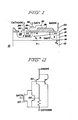
- the lateral insulated gate transistor 10 of a conventional type is shown in Figure 1.
- the device comprises a lightly doped P substrate 12 having a N type layer 14 epitaxially disposed thereon.
- An N type buffer region 16 is disposed in the layer 14 and a P+ anode region 18 is disposed within the N buffer region 16.
- a metallized contact 20 is applied to the P+ anode region 18 and a terminal 22 is electrically connected to the metallized layer 20.
- a F base region 28 is disposed in the epitaxial layer 14 and an N; cathode region 30 is disposed within the P base 28.
- a metal contact 32 is disposed over and in contact with the N+ cathode region 30 and the P base region 28 and serves as an electrical contact for each region and additionally shorts the source region 30 to the base region 28.
- a terminal 34 is applied to the cathode contact 32.
- the cathode portion of the device is separated from the anode portion of the device by a portion of the epitaxial layer which is designated as the N- drift layer.
- the surface of the device 10 is formed by a portion of the epitaxial layer 14, the anode region 18, the buffer region 16, the base region 28 and source region 30.
- An insulation layer 36 is disposed over a portion of the base region 28 and a portion of the source region 30.
- a gate electrode is disposed over the insulation layer in registry with a portion of the base region 28 such that upon appropriate biasing, the gate 38 induces a channel in the base region having a capability to conduct a substantially all of majority carrier, or electron current in this example, from the cathode electrode 32 into the drift region 14 .
- a metallized gate electrode 40 is applied to the gate member 38 and a gate terminal 42 can be applied to the gate electrode.
- device current essentially comprises three separate components.
- the first component might be considered the majority carrier current comprising in this example electrons flowing from the cathode electrode 32 through the source region 30, through a N- type channel induced in the P base region 28 into the N drift layer 14 and possibly the N buffered region 16 to recombine with holes injected into the N buffer layer 16 and the N drift layer 14 from the anode terminal 20.
- a second component of the device current comprises the lateral hole current flowing from the P+ anode 18 through the N buffer region 16, the N drift region 14 into the P base region 28 laterally beneath the source region 30 and parallel to the surface of the device and then continuing in the base region 28 transverse to the plane of the surface of the device to the cathode terminal 32.
- a still further vertical component of the device current is established by the inherent PNP transistor existing between the anode terminal 20, the N buffer region 16 and the P substrate 12 when the P substrate is tied to a source of charge carrier such as ground.
- an equivalent circuit diagram of a typical insulated gate'transistor is shown in schematic form to include a field effect transistor 50 connected between the cathode terminal 34 and the N drift region 14.
- An NPN transistor 52 comprising source region 30, base region 28, and drift region 14 is coupled between the cathode electrode 34 and the N base region 14 of a PNP transistor 55.
- the PNP transistor 55 accounts for the lateral hole current flow and is illustrated to comprise the P+ anode region 18 as the emitter, the N buffer region 16 in combination with the N drift region 14 as the base, and the P base region 28 as the lateral hole collector.
- the collector of the PNP transistor 55 is coupled to the base of the NPN electron transistor 52 and also to the cathode through a symbolic resistance R indicative of the resistance in base region 28.
- PNP transistor 57 is responsible for the control of vertical hole current and has as its emitter P+ anode region 18 which is coupled to the anode terminal, the N buffer region 16 as its base, and the P- substrate 12 as its collector which is coupled to ground.
- the device includes an anode terminal 22, an anode contact 20, a P+ anode region 18, a lightly doped N buffer region 16, an N drift region 14, a P base region 28, and N+ source region 30, a cathode contact 32, and a cathode terminal 34.
- the aforesaid lateral insulated gate transistor is disposed not a on a P-substrate 12 alone, but instead on the P* substrate 60 with a F- layer 62 epitaxially disposed thereon.
- the P* substrate provides a drain or sink for holes or minority carriers and has been found to contribute substantially to the collector current of the vertical transistor 57 and thus contribute substantially to the vertical component of the hole current operating in a lateral insulated gate transistor 10.
- the P+ substrate 60 is tied to a sink,for hole carriers such as ground.
- the gate insulation layer 36 can be extended over 'the N buffer region 16 and the anode region 18 to ensure that surface contamination does not inadvertently lead to shcrting of the junction between the F+ region 18 and the N buffer region 16.
- the N buffer region is provided to avoid punch through between the P+ anode and the P- epitaxial layer.
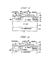
- an improved lateral insulated gate transistor 10 in accordance with the present invention is shown in an alternate preferred embodiment.
- this device is illustrated to have been fabricated on a P- substrate 12, it will be recognized that a similar device can be fabricated on a P+ substrate 60 such as that employed in Figure 3, to avail the device of the enhanced vertical hole current associated with the P+ substrate 60.
- buffer 16, drift 14, base 28, source 30, and gate 40 regions an additional P+ current control region 66 is disposed within the F- substrate 12 and the N drift region 14 and overlaps a portion of the P base 28 and the N+ source 30.
- the P+ region can be established by diffusion after an epitaxial growth of the N- layer and prior to the diffusion of the P base 28 or the N+ source region 30.
- a major portion or substantially all of the P+ conductive region 66 does not underlie a major portion of the source region 30 and accordingly, has little or no effect on the lateral resistance of the minority carrier current path existing in the P base 30 beneath the source region 30.
- the highly conductive region 66 predominantly impacts upon that portion of the minority carrier current path transverse to the surface of the device existing between the cathode terminal 32 and the interface between the highly conductive region 66 and the P base 28. More particularly, the transverse portion of the minority carrier current path is rendered highly conductive by virtue of the overlap with the highly conductive region thus is less resistive. Accordingly, the IR voltage drop along this portion of the minority carrier path is reduced or is less than that which might otherwise be expected without this highly conductive region. Accordingly, the voltage drop along the interface between the P base region 28 and the N+ source region 30 is reduced providing that device with improved latching immunity.
- FIG. 5 A still further alternate embodiment of the lateral insulated gate transistor 10 in accordance with the present invention is shown in Figure 5 in cross-sectional form.
- the embodiment of Figure 5 can alternately be disposed on a P+ substrate to attain the benefits of the F+ substrate carrier injection contributing to an improvement in the vertical component of the hole current.
- the embodiment of Figure 5 has been illustrated on a P- substrate 12. Again, given the similarity in appearance of the various regions of the device, like reference numerals have been carried forward to facilitate rapid understanding of the invention disclosed herein.
- the device includes an anode terminal 22, an anode contact 20, an anode region 18, an N buffer region 16, an N drift region 14, a P base 28, an N+ source region 30, a cathode contact 32 and a cathode terminal 34.
- an insulation layer 36 is disposed over a portion of the P base region 28 and the gate electrode 38 is disposed over a portion of the insulation layer 36 in registry with the P base 28.
- the gate electrode 40 is applied to the gate 38 and a gate terminal 42 is applied to the gate electrode 40.
- the P- substrate is provided with a P+ buried layer 70 early in the fabrication process, as by diffusion.
- an N-layer 14 is preferably formed epitaxially on a P-substrate 12.
- the P+ buried layer is then diffused into the N- layer 14 so as to extend the P+ buried layer into the N- drift region 14 and form a graded junction with the P base region 28.
- a P base region 28 can be diffused from the upper surface of the epitaxial layer 14 and similarly, an N+ source region 30 can-be diffused within the base region.
- the highly conductive region, or buried layer 70 underlies substantially the entire P base region, but does not substantially overlap therewith.
- the buried layer 70 which extends partially into P region 28, establishes a conductive path which is separated and spaced away from the base/source junction.
- lateral hole current flowing through the N drift layer which mightotherwise flow in the less conductive P base region 28 is induced to flow primarily through the highly conductive region 70 to laterally traverse a substantial portion of the base region 38.
- the N+ source region 30 shields a portion of the cathode contact 32 and thus carriers flowing in the lateral path of the buried region 70 are not influenced by the potential applied to the metal contact 32 which has thus been shielded. Accordingly, the highly conductive buried layer 70 provides a lateral current path from the edge of the P base region 28 to approximately the edge of the N + region which is shielded from the cathode terminal potential. The minority carriers flow along a lateral path is substantially parallel tc the surface of the device laterally beneath the P+ base portion of P base region 28.
- the P+ buried layer 70 provides a highly conductive lateral current path having a low resistivity.
- the voltage drop across the minority carrier current path through the P- buried region 70 is less than the drop which would otherwise occur in the P base region 28 under the conditions of the same current flow. Further, the voltage drop that does occur, is exhibited in the highly conductive region 70 and not along the junction between the source 3C and P base 28.
- the highly conductive P+ buried layer provides a reduced voltage drop along the PN junction between the P base 2E and the source region 30.
- the device 10 therefore exhibits a reduced tendency to latch or improve latching immunity. It has been found that the present embodiment involving the P+ buried layer provides a substantial improvement in the latching immunity of the device, and accordingly, is particularly preferred and is considered to provide a device which is current- limited by the channel conductivity rather than by the latching threshold.
- Figure 6 a computer model of the total current flow pattern of the device 10 is illustrated as superimposed in various device regions. More particularly, Figure 6 represents a conventional lateral insulated gate transistor 10 such as that shown in Figure 1.
- the device current as discussed above, includes bilateral current flow between the source 30 and anode 20 terminals as well as a vertical component of minority carrier current flowing between the anode and substrate and a horizontal component of minority carrier current flowing between the anode and cathode. It is seen that a substantial portion of the hole current flows through the P base region 28 in Figure 6.
- FIG 7 a similar current flow pattern plot made with respect to the embodiment of Figure 5 is seen.
- This figure shows a dramatic change in the flow of hole current. More particularly, hole current is seen to flow through the highly conductive region 70 laterally beneath and spaced from the PN base region 28 and the junction between the base region 28 and the source region 30. Accordingly, the voltage drop along the PN junction 28/30 is reduced contributing to improved latching immunity in the device.
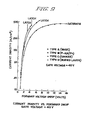
- Figure 8 is an illustration of a comparison of the current density vs. forward drop characteristics cf typical devices constructed in accordance with Figures 1, 3, 4, and 5 hereof and operated at gate voltages of 20 volts.
- devices of the type shown in Figures 1 and 3 operated at current. densities in the order of 200-300 A/cm 2 .
- devices of the type illustrated in Figures 4 and 5 did not latch, but instead, the current of these devices is saturated.
- Figure 9 is an illustration of a comparison 10 of the current density vs. forward drop characteristics of typical devices in accordance with Figures 1, 3, 4, and 5 operated at a gate voltage of 40 volts.
- devices of the type shown in Figures 1, 3, and 5 were operated at increased current densities 15 before latch occurred.
- devices of the type illustrated in Figure 5 did not latch, but instead, the current of this device is saturated.
- FIG. 10 a particularly preferred embodiment of the lateral insulated gate transistor 10 of the present invention is illustrated in cross-section.
- This embodiment combines the 30 beneficial features and aspects of the Figures 3, 4, and 5 embodiment to provide a device 10 having particularly enhanced current conducting capacity or improved current density as well as improved immunity to latching.
- This embodiment includes a heavily doped substrate layer 60 of one conductivity, such as the illustrated P+ layer having a thickness typically in the order of 20 mils.
- the heavily doped substrate layer 6C was discussed above in relation to Figure 3, as providing, when connected to an appropriate potential, a drain for minority carriers or holes in the lateral device 10 to substantially increase the vertical component of the hole minority carrier current in the illustrated device.
- the device of Figure 10 combines the heavily doped region 66 of Figure 4 with the buried layer of Figure 5 to reduce the resistivity of the base region and also provide an additional region separated or spaced from the base region, which additional region is highly conductive to minority carriers or holes in the illustrated example to divert holes away from the source 30, reducing the base/source junction IR voltage significantly. In this manner, the voltage drop across any portion of the source base junction is maintained at a voltage level well below the injection threshold, approximately .7 volts for silicon devices, necessary for the device to enter into regenerative latch-up and triggering the inherent four layer parasitic element of the device.
- the heavily doped region 80 covers all surfaces of the base region other than the surface forming the surface of the device and a portion of the base drift junction interfacting the drift layer to the channel.
- the combination of the highly doped region 66 with the buried layer 70 effectively alters and increases the conductivity of substantially the entire base region 28, except in a limited region of the P-base 26 surrounding the gate induced channel portion.
- the reduced resistivity or increased conductivity of the base region 28 abutting substantially all of the source region 30 consequently causes a reduced IR voltage drop along the base/source junction making the device less likely to latch at a given device current level. More importantly, however, reduced resistivity along the base/source junction allows the current level through the region 28 to be increased without increasing the IR voltage along the base/source junction to a level in excess of the forward bias or injection potential of the base/source junction.
- region 70 establishes a highly conductive current path for minority carriers of the device, holes in the illustrated example, which most holes, traveling in the drift region 14 prefer over the corresponding path in the base 28. Accordingly, the heavily doped region 70 diverts holes away from the base region 28 to thereby reduce the I component of the I component of the IR voltage drop occurring along the base/source junction.
- the combination of both the reduced resistivity current path adjacent a substantial portion of the base/source junction and the reduction of hole current flowing in this path proportionately increases the amount of hole or minority carrier current which can flow between the anode and cathode of the device. Accordingly, the more current can flow through the device allowing the device to be operated at current densities well in excess of 500 A/cm 2 and approaching 1000 A / cm 2.
- the resistivity of the base region 28 is lowered to such an extent, and the additional heavily doped region 70 diverts holes to an extent that the tendency of the base/source junction to latch is no longer the limiting factor of the device. Instead, the current capacity of the gate induced channel saturates or establishes the maximum current level of the device.
- the lateral insulated gate transistor device with the buried layer 70 and heavily doped region 66 is shown on a dielectrically isolated substrate.
- the lateral insulated gate transistor structure without the buried layer 70 and the heavily doped region 66 would latch at a substantially lower current as the vertical current component for the junction isolated substrate is now absent. All the anode current is collected laterally by the cathode at the top surface of the device.
- the buried layer 70 and P* heavily doped region 66 provides a low resistance path for the holes as discussed earlier and thus reducing the forward biasing of the source/base junction. This results in a lateral insulated gate transistor with improved current density and increased immunity from latch-up.
- the structures described in Figures 7 and 8 can be realized by dielectric isolation process or alternatively a semiconductor on insulator process.
- the F* buried layer is implanted/diffused prior to the growth of the isolating oxide and growth of the polysilicon substrate.
- the first layer over the isolating oxide must be kept thin ( ⁇ 1 ⁇ m) during the semiconductor insulator process. In most of the candidate semiconductor on insulator processes (buried oxide or recrystallization) this tends to occur naturally.
- the P+ buried layer would then be implanted/diffused and an epitaxial layer subsequently grown on top.
- a lateral insulated gate transistor exhibiting a 350 volt forward voltage blocking peak in accordance with the present invention can be fabricated by conventional diffusion techniques discussed, for instance, by A.S. Grove, Physics and Technology of Semiconductor Devices, pages 35-78. More specifically, the P+ substrate 12 is heavily doped to ; approximately 1E19 atom/cc.
- the P- epitaxial layer 14 can be grown thereon and has a doping concentration of 2E14 atom/cc/ A buried region 70 with Peak doping density of the order of IE18 A/cc is typically estab-lished in the substrate layer prior to formation of the epitaxial layer 14.
- the P base region 28 typically has a conductivity of 1E17 atom/cc while the source region 30 typically has a conductivity of approximately 5E19 atom / cc.
- the N buffer region 14 can have a conductive of approximately 5E14 atom/cc.
- the width of the buffer region is typically 25 microns and can be increa.sed to, for instance, increase the beta of the device. For instance, a 35 micron device has a forward blocking voltage of approximately 500 volts.
- the insulation layer is typically 1000 Angstroms overlying the base and source regions and 7500 Angstroms overlying the drift region.
- the gate metal is typically 5000 Angstroms thick.
- a method of forming an insulated gate transistor exhibiting improved currently conductivity and improved latching and having a substantially planar surface in accordance with the present invention includes the steps of providing a heavily doped substrate layer of said one type conductivity such as P type conductivity, establishing a heavily doped buried region of said one type conductivity in said substrate layer; forming a first lightly doped layer of the one conductivity on the substrate; forming a second lightly doped layer of the opposite type conductivity on the first layer; establishing a first region of the opposite type conductivity in the second lightly doped layer, the first region forming a portion of the substantially planar surface, establishing a second regin of the one type conductivity in the first region, the second region forming a portion of the substantially planar surface; establishing a third region of the one type conductivity such as P type conductivity, establishing a heavily doped buried region of said one type conductivity in said substrate layer; forming a first lightly doped layer of the one conductivity on the substrate; forming a second lightly doped
- the conductive path is formed substantially parallel to the substantially planar surface.
- a heavily doped diffused region is substituted for the heavily doped buried region.
- the conductive path formed by this method is substantially transverse to the substantially planar surface of the device.
- the lateral insulated gate transistor has been described in a preferred embodiment, the invention self is not so limited. Variations of the disclosed insulated gate device will be readily apparent to those in the art. More particularly, the relative size, conductivity, and configuration of the device layers and regions can be varied over a broad range without departing from the spirit and scope of this invention. Further, the gate insulation and overlying gate layer can extend farther into the N source region 30 or N- drift region 14. While the substrate is shown as being coupled to ground, an alternate bias source can be employed to appropriately bias the vertical transistor 57.
Landscapes
- Insulated Gate Type Field-Effect Transistor (AREA)
- Thyristors (AREA)
Applications Claiming Priority (2)
| Application Number | Priority Date | Filing Date | Title |
|---|---|---|---|
| US06/803,049 US4963951A (en) | 1985-11-29 | 1985-11-29 | Lateral insulated gate bipolar transistors with improved latch-up immunity |
| US803049 | 1985-11-29 |
Publications (3)
| Publication Number | Publication Date |
|---|---|
| EP0224269A2 true EP0224269A2 (de) | 1987-06-03 |
| EP0224269A3 EP0224269A3 (en) | 1989-02-22 |
| EP0224269B1 EP0224269B1 (de) | 1992-10-14 |
Family
ID=25185454
Family Applications (1)
| Application Number | Title | Priority Date | Filing Date |
|---|---|---|---|
| EP86116513A Expired EP0224269B1 (de) | 1985-11-29 | 1986-11-27 | Lateraler Transistor mit isoliertem Gate mit Latch-up-Festigkeit |
Country Status (4)
| Country | Link |
|---|---|
| US (1) | US4963951A (de) |
| EP (1) | EP0224269B1 (de) |
| JP (1) | JPH0758784B2 (de) |
| DE (1) | DE3686971T2 (de) |
Cited By (6)
| Publication number | Priority date | Publication date | Assignee | Title |
|---|---|---|---|---|
| FR2607324A1 (fr) * | 1986-11-26 | 1988-05-27 | Gen Electric | Transistor a grille isolee avec diode verticale integree et procede de fabrication |
| US4926074A (en) * | 1987-10-30 | 1990-05-15 | North American Philips Corporation | Semiconductor switch with parallel lateral double diffused MOS transistor and lateral insulated gate transistor |
| US4939566A (en) * | 1987-10-30 | 1990-07-03 | North American Philips Corporation | Semiconductor switch with parallel DMOS and IGT |
| US5237186A (en) * | 1987-02-26 | 1993-08-17 | Kabushiki Kaisha Toshiba | Conductivity-modulation metal oxide field effect transistor with single gate structure |
| EP0497577B1 (de) * | 1991-01-31 | 2002-07-17 | Kabushiki Kaisha Toshiba | Halbleiterbauelement für hohe Durchbruchsspannungen |
| WO2006123105A3 (en) * | 2005-05-20 | 2007-04-19 | Cambridge Semiconductor Ltd | Semiconductor device and method of forming a semiconductor device |
Families Citing this family (51)
| Publication number | Priority date | Publication date | Assignee | Title |
|---|---|---|---|---|
| US5258641A (en) * | 1989-12-28 | 1993-11-02 | Mitsubishi Denki Kabushiki Kaisha | Semiconductor device for extracting a signal used to monitor potential of a high voltage island at a low voltage island and method of manufacturing the same |
| JP2513874B2 (ja) * | 1989-12-28 | 1996-07-03 | 三菱電機株式会社 | 半導体装置およびその製造方法 |
| JP3190057B2 (ja) * | 1990-07-02 | 2001-07-16 | 株式会社東芝 | 複合集積回路装置 |
| US5290396A (en) * | 1991-06-06 | 1994-03-01 | Lsi Logic Corporation | Trench planarization techniques |
| US5413966A (en) * | 1990-12-20 | 1995-05-09 | Lsi Logic Corporation | Shallow trench etch |
| US5072268A (en) * | 1991-03-12 | 1991-12-10 | Power Integrations, Inc. | MOS gated bipolar transistor |
| US5252503A (en) * | 1991-06-06 | 1993-10-12 | Lsi Logic Corporation | Techniques for forming isolation structures |
| US5225358A (en) * | 1991-06-06 | 1993-07-06 | Lsi Logic Corporation | Method of forming late isolation with polishing |
| US5248625A (en) * | 1991-06-06 | 1993-09-28 | Lsi Logic Corporation | Techniques for forming isolation structures |
| EP0522712B1 (de) * | 1991-06-10 | 1999-03-24 | Kabushiki Kaisha Toshiba | Thyristor mit isoliertem Gate |
| US5428228A (en) * | 1991-06-10 | 1995-06-27 | Kabushiki Kaisha Toshiba | Method of operating thyristor with insulated gates |
| US5227653A (en) * | 1991-08-07 | 1993-07-13 | North American Philips Corp. | Lateral trench-gate bipolar transistors |
| JPH05206469A (ja) * | 1992-01-29 | 1993-08-13 | Hitachi Ltd | 絶縁ゲート型バイポーラトランジスタ |
| US5378912A (en) * | 1993-11-10 | 1995-01-03 | Philips Electronics North America Corporation | Lateral semiconductor-on-insulator (SOI) semiconductor device having a lateral drift region |
| JPH08139319A (ja) * | 1994-11-11 | 1996-05-31 | Mitsubishi Electric Corp | 半導体装置およびその製造方法 |
| JPH08227999A (ja) * | 1994-12-21 | 1996-09-03 | Mitsubishi Electric Corp | 絶縁ゲート型バイポーラトランジスタ及びその製造方法並びに半導体集積回路及びその製造方法 |
| EP0761016B1 (de) * | 1995-03-23 | 2002-10-16 | Koninklijke Philips Electronics N.V. | Halbleiteranordnung mit einem ligbt element |
| US6831331B2 (en) | 1995-11-15 | 2004-12-14 | Denso Corporation | Power MOS transistor for absorbing surge current |
| DE19725091B4 (de) * | 1997-06-13 | 2004-09-02 | Robert Bosch Gmbh | Laterales Transistorbauelement und Verfahren zu seiner Herstellung |
| US6054365A (en) * | 1998-07-13 | 2000-04-25 | International Rectifier Corp. | Process for filling deep trenches with polysilicon and oxide |
| DE19904103B4 (de) * | 1999-02-02 | 2005-04-14 | Infineon Technologies Ag | IGBT mit verbesserter Durchlaßspannung |
| US6191453B1 (en) | 1999-12-13 | 2001-02-20 | Philips Electronics North America Corporation | Lateral insulated-gate bipolar transistor (LIGBT) device in silicon-on-insulator (SOI) technology |
| US6413806B1 (en) * | 2000-02-23 | 2002-07-02 | Motorola, Inc. | Semiconductor device and method for protecting such device from a reversed drain voltage |
| US6768171B2 (en) | 2000-11-27 | 2004-07-27 | Power Integrations, Inc. | High-voltage transistor with JFET conduction channels |
| US6509220B2 (en) | 2000-11-27 | 2003-01-21 | Power Integrations, Inc. | Method of fabricating a high-voltage transistor |
| US6424007B1 (en) | 2001-01-24 | 2002-07-23 | Power Integrations, Inc. | High-voltage transistor with buried conduction layer |
| US7221011B2 (en) * | 2001-09-07 | 2007-05-22 | Power Integrations, Inc. | High-voltage vertical transistor with a multi-gradient drain doping profile |
| US7786533B2 (en) | 2001-09-07 | 2010-08-31 | Power Integrations, Inc. | High-voltage vertical transistor with edge termination structure |
| US6573558B2 (en) * | 2001-09-07 | 2003-06-03 | Power Integrations, Inc. | High-voltage vertical transistor with a multi-layered extended drain structure |
| US6635544B2 (en) | 2001-09-07 | 2003-10-21 | Power Intergrations, Inc. | Method of fabricating a high-voltage transistor with a multi-layered extended drain structure |
| US6555873B2 (en) * | 2001-09-07 | 2003-04-29 | Power Integrations, Inc. | High-voltage lateral transistor with a multi-layered extended drain structure |
| JP2004335990A (ja) * | 2003-03-10 | 2004-11-25 | Fuji Electric Device Technology Co Ltd | Mis型半導体装置 |
| JP4547872B2 (ja) * | 2003-06-13 | 2010-09-22 | 日本ビクター株式会社 | スイッチング素子の製造方法 |
| KR100618775B1 (ko) * | 2004-12-31 | 2006-08-31 | 동부일렉트로닉스 주식회사 | 반도체 소자 |
| US7466006B2 (en) * | 2005-05-19 | 2008-12-16 | Freescale Semiconductor, Inc. | Structure and method for RESURF diodes with a current diverter |
| US7439584B2 (en) * | 2005-05-19 | 2008-10-21 | Freescale Semiconductor, Inc. | Structure and method for RESURF LDMOSFET with a current diverter |
| JP2007194575A (ja) * | 2005-12-21 | 2007-08-02 | Mitsubishi Electric Corp | 半導体装置 |
| US7465964B2 (en) * | 2005-12-30 | 2008-12-16 | Cambridge Semiconductor Limited | Semiconductor device in which an injector region is isolated from a substrate |
| JP2008124421A (ja) * | 2006-10-17 | 2008-05-29 | Matsushita Electric Ind Co Ltd | 半導体装置及びその製造方法 |
| US7531888B2 (en) * | 2006-11-30 | 2009-05-12 | Fairchild Semiconductor Corporation | Integrated latch-up free insulated gate bipolar transistor |
| JP5191132B2 (ja) * | 2007-01-29 | 2013-04-24 | 三菱電機株式会社 | 半導体装置 |
| US7859037B2 (en) | 2007-02-16 | 2010-12-28 | Power Integrations, Inc. | Checkerboarded high-voltage vertical transistor layout |
| US7557406B2 (en) | 2007-02-16 | 2009-07-07 | Power Integrations, Inc. | Segmented pillar layout for a high-voltage vertical transistor |
| US7595523B2 (en) | 2007-02-16 | 2009-09-29 | Power Integrations, Inc. | Gate pullback at ends of high-voltage vertical transistor structure |
| US7468536B2 (en) | 2007-02-16 | 2008-12-23 | Power Integrations, Inc. | Gate metal routing for transistor with checkerboarded layout |
| US8653583B2 (en) | 2007-02-16 | 2014-02-18 | Power Integrations, Inc. | Sensing FET integrated with a high-voltage transistor |
| CN100592532C (zh) * | 2007-08-28 | 2010-02-24 | 电子科技大学 | 具有“u”字形漂移区的半导体器件 |
| JP4767264B2 (ja) * | 2008-01-15 | 2011-09-07 | 三菱電機株式会社 | 高耐圧半導体装置 |
| US10325988B2 (en) | 2013-12-13 | 2019-06-18 | Power Integrations, Inc. | Vertical transistor device structure with cylindrically-shaped field plates |
| US9543396B2 (en) | 2013-12-13 | 2017-01-10 | Power Integrations, Inc. | Vertical transistor device structure with cylindrically-shaped regions |
| CN115917971A (zh) | 2020-05-14 | 2023-04-04 | 康明斯公司 | 去抖动固态开关器件 |
Family Cites Families (16)
| Publication number | Priority date | Publication date | Assignee | Title |
|---|---|---|---|---|
| US3697830A (en) * | 1964-08-10 | 1972-10-10 | Gte Sylvania Inc | Semiconductor switching device |
| JPS5123432B2 (de) * | 1971-08-26 | 1976-07-16 | ||
| US4199774A (en) * | 1978-09-18 | 1980-04-22 | The Board Of Trustees Of The Leland Stanford Junior University | Monolithic semiconductor switching device |
| NL186665C (nl) * | 1980-03-10 | 1992-01-16 | Philips Nv | Halfgeleiderinrichting. |
| US4364073A (en) * | 1980-03-25 | 1982-12-14 | Rca Corporation | Power MOSFET with an anode region |
| US4300150A (en) * | 1980-06-16 | 1981-11-10 | North American Philips Corporation | Lateral double-diffused MOS transistor device |
| JPS57211778A (en) * | 1981-06-24 | 1982-12-25 | Hitachi Ltd | Mos semiconductor device |
| US4503598A (en) * | 1982-05-20 | 1985-03-12 | Fairchild Camera & Instrument Corporation | Method of fabricating power MOSFET structure utilizing self-aligned diffusion and etching techniques |
| US4443931A (en) * | 1982-06-28 | 1984-04-24 | General Electric Company | Method of fabricating a semiconductor device with a base region having a deep portion |
| US4532534A (en) * | 1982-09-07 | 1985-07-30 | Rca Corporation | MOSFET with perimeter channel |
| JPS5955052A (ja) * | 1982-09-24 | 1984-03-29 | Hitachi Ltd | 半導体集積回路装置の製造方法 |
| EP0111803B1 (de) * | 1982-12-13 | 1989-03-01 | General Electric Company | Laterale Gleichrichter mit isoliertem Gate |
| US4639761A (en) * | 1983-12-16 | 1987-01-27 | North American Philips Corporation | Combined bipolar-field effect transistor resurf devices |
| US4587713A (en) * | 1984-02-22 | 1986-05-13 | Rca Corporation | Method for making vertical MOSFET with reduced bipolar effects |
| JPS60196974A (ja) * | 1984-03-19 | 1985-10-05 | Toshiba Corp | 導電変調型mosfet |
| US4609929A (en) * | 1984-12-21 | 1986-09-02 | North American Philips Corporation | Conductivity-enhanced combined lateral MOS/bipolar transistor |
-
1985
- 1985-11-29 US US06/803,049 patent/US4963951A/en not_active Expired - Lifetime
-
1986
- 1986-11-25 JP JP61278905A patent/JPH0758784B2/ja not_active Expired - Fee Related
- 1986-11-27 DE DE8686116513T patent/DE3686971T2/de not_active Expired - Fee Related
- 1986-11-27 EP EP86116513A patent/EP0224269B1/de not_active Expired
Cited By (6)
| Publication number | Priority date | Publication date | Assignee | Title |
|---|---|---|---|---|
| FR2607324A1 (fr) * | 1986-11-26 | 1988-05-27 | Gen Electric | Transistor a grille isolee avec diode verticale integree et procede de fabrication |
| US5237186A (en) * | 1987-02-26 | 1993-08-17 | Kabushiki Kaisha Toshiba | Conductivity-modulation metal oxide field effect transistor with single gate structure |
| US4926074A (en) * | 1987-10-30 | 1990-05-15 | North American Philips Corporation | Semiconductor switch with parallel lateral double diffused MOS transistor and lateral insulated gate transistor |
| US4939566A (en) * | 1987-10-30 | 1990-07-03 | North American Philips Corporation | Semiconductor switch with parallel DMOS and IGT |
| EP0497577B1 (de) * | 1991-01-31 | 2002-07-17 | Kabushiki Kaisha Toshiba | Halbleiterbauelement für hohe Durchbruchsspannungen |
| WO2006123105A3 (en) * | 2005-05-20 | 2007-04-19 | Cambridge Semiconductor Ltd | Semiconductor device and method of forming a semiconductor device |
Also Published As
| Publication number | Publication date |
|---|---|
| JPS62189758A (ja) | 1987-08-19 |
| DE3686971T2 (de) | 1993-04-29 |
| EP0224269B1 (de) | 1992-10-14 |
| US4963951A (en) | 1990-10-16 |
| DE3686971D1 (de) | 1992-11-19 |
| EP0224269A3 (en) | 1989-02-22 |
| JPH0758784B2 (ja) | 1995-06-21 |
Similar Documents
| Publication | Publication Date | Title |
|---|---|---|
| US4963951A (en) | Lateral insulated gate bipolar transistors with improved latch-up immunity | |
| US4821095A (en) | Insulated gate semiconductor device with extra short grid and method of fabrication | |
| EP0990268B1 (de) | Bipolar mos-leistungstransistor ohne latch-up | |
| US6051850A (en) | Insulated gate bipolar junction transistors having built-in freewheeling diodes therein | |
| US7795638B2 (en) | Semiconductor device with a U-shape drift region | |
| US4989058A (en) | Fast switching lateral insulated gate transistors | |
| GB2111745A (en) | Insulated-gate field-effect transistors | |
| EP0185415B1 (de) | Kombinierter lateraler MOS/bipolarer Transistor hoher Leitfähigkeit | |
| US5430323A (en) | Injection control-type Schottky barrier rectifier | |
| EP0522670B1 (de) | Schnellschaltender, lateraler Feldeffekttransistor mit isolierter Steuerelektrode | |
| JPH0457111B2 (de) | ||
| EP0503605B1 (de) | Bipolarer Transistor vom isolierten Gatetyp mit Überspannungschutz | |
| EP0071335B1 (de) | Feldeffekttransistor | |
| EP0338312B1 (de) | Bipolarer Transistor mit isolierter Steuerelektrode | |
| US5079607A (en) | Mos type semiconductor device | |
| JP2590863B2 (ja) | 導電変調型mosfet | |
| EP0761016B1 (de) | Halbleiteranordnung mit einem ligbt element | |
| US6180959B1 (en) | Static induction semiconductor device, and driving method and drive circuit thereof | |
| US12432950B2 (en) | Insulated gate bipolar transistor including trench Schottky electrode | |
| EP0555047B1 (de) | Schaltungs-Halbleiterbauteil mit Gate | |
| US6147382A (en) | Semiconductor switching device with segmented sources | |
| JPS63173365A (ja) | ラテラル形絶縁ゲート半導体装置とその製法 | |
| CN101512738B (zh) | 半导体器件和形成半导体器件的方法 | |
| US20230163167A1 (en) | Semiconductor device including a trench gate structure | |
| JPH02208976A (ja) | 電導度変調型mosfet |
Legal Events
| Date | Code | Title | Description |
|---|---|---|---|
| PUAI | Public reference made under article 153(3) epc to a published international application that has entered the european phase |
Free format text: ORIGINAL CODE: 0009012 |
|
| AK | Designated contracting states |
Kind code of ref document: A2 Designated state(s): DE NL |
|
| PUAL | Search report despatched |
Free format text: ORIGINAL CODE: 0009013 |
|
| AK | Designated contracting states |
Kind code of ref document: A3 Designated state(s): DE NL |
|
| 17P | Request for examination filed |
Effective date: 19890802 |
|
| 17Q | First examination report despatched |
Effective date: 19910214 |
|
| GRAA | (expected) grant |
Free format text: ORIGINAL CODE: 0009210 |
|
| AK | Designated contracting states |
Kind code of ref document: B1 Designated state(s): DE NL |
|
| REF | Corresponds to: |
Ref document number: 3686971 Country of ref document: DE Date of ref document: 19921119 |
|
| PLBE | No opposition filed within time limit |
Free format text: ORIGINAL CODE: 0009261 |
|
| STAA | Information on the status of an ep patent application or granted ep patent |
Free format text: STATUS: NO OPPOSITION FILED WITHIN TIME LIMIT |
|
| 26N | No opposition filed | ||
| NLS | Nl: assignments of ep-patents |
Owner name: HARRIS CORPORATION TE MELBOURNE, FLORIDA, VER. ST. |
|
| PGFP | Annual fee paid to national office [announced via postgrant information from national office to epo] |
Ref country code: NL Payment date: 19951024 Year of fee payment: 10 |
|
| PG25 | Lapsed in a contracting state [announced via postgrant information from national office to epo] |
Ref country code: NL Effective date: 19970601 |
|
| NLV4 | Nl: lapsed or anulled due to non-payment of the annual fee |
Effective date: 19970601 |
|
| PGFP | Annual fee paid to national office [announced via postgrant information from national office to epo] |
Ref country code: DE Payment date: 20021202 Year of fee payment: 17 |
|
| PG25 | Lapsed in a contracting state [announced via postgrant information from national office to epo] |
Ref country code: DE Free format text: LAPSE BECAUSE OF NON-PAYMENT OF DUE FEES Effective date: 20040602 |