EP0225159A2 - Bildkantendetektionssystem - Google Patents
Bildkantendetektionssystem Download PDFInfo
- Publication number
- EP0225159A2 EP0225159A2 EP86309195A EP86309195A EP0225159A2 EP 0225159 A2 EP0225159 A2 EP 0225159A2 EP 86309195 A EP86309195 A EP 86309195A EP 86309195 A EP86309195 A EP 86309195A EP 0225159 A2 EP0225159 A2 EP 0225159A2
- Authority
- EP
- European Patent Office
- Prior art keywords
- signal
- data
- detecting
- image
- producing
- Prior art date
- Legal status (The legal status is an assumption and is not a legal conclusion. Google has not performed a legal analysis and makes no representation as to the accuracy of the status listed.)
- Withdrawn
Links
Images

Classifications
-
- G—PHYSICS
- G06—COMPUTING OR CALCULATING; COUNTING
- G06T—IMAGE DATA PROCESSING OR GENERATION, IN GENERAL
- G06T9/00—Image coding
- G06T9/20—Contour coding, e.g. using detection of edges
Definitions
- This invention relates to a system for detecting an edge of an image of an object, for example, being transported on a belt conveyer, so as to determine the shape and posture of the object or to inspect such an object.
- FIG. 2 shows a block diagram of a system for detecting such level-varying points.
- This image edge- detecting system will now be described.
- a composite video signal VE is fed from a video camera 10 to a synchronizing separator circuit 12 which separates a vertical synchronizing signal VD and a horizontal synchronizing signal HD from the composite video signal VE and outputs these separated synchronizing signals along with an image signal Vs.
- the image signal Vs is converted by a converter circuit 14 into a binary image signal Vb representative of the image of the object to be inspected.
- the image-edge detection system shown in Fig. 2 comprises a 2-bit shift register 16, an exclusive OR gate 18, an inverter 20, a NAND gate 22, three counters 24, 26 and 28, and a memory 30.
- the level-varying points on the edge of the binary image signal Vb are detected through the shift register 16 and the exclusive OR gate 18, and a write enable signal WE of the low level is fed from the NAND gate 22 to a write terminal W of the memory 30 in synchronizing with a trailing edge of a clock pulse SC, so that X coordinate data outputted from the counter 24 and representing the X coordinate of the level-varying point is loaded onto the memory 30.
- Y coordinate data outputted from the counter 26 and representing the Y coordinate of the level-varying point is loaded onto the memory 30.
- the address of the memory 30 into which the X and Y coordinate data are to be written are designated by the output of the address counter 28.
- the X coordinate data (column position data) and Y coordinate data (row position data) of each level-varying point on the edge of the image are stored in the memory 30. Therefore, the Y coordinate data of the varying points on a common row or horizontal scanning line are equal in value. Thus, the Y coordinate data of the same value are stored in the memory 30, so that the capacity of the memory 12 must be correspondingly increased, and in addition the time required for data processing by the computer is prolonged.
- a system for detecting an edge of an image comprising:
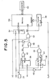
- Clock pulses SC are generated from a timing signal generator 34.
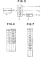
- a binary image signal Vb derived from a composite video signal as described above, is fed to a data input terminal A of a 2-bit shift register 36, and the binary image data Vb is loaded onto the shift register 36 and is outputted from a first output terminal QA of the shift register 36 when a clock pulse SC is applied to a clock terminal CK of the shift register 36. Then, when the next clock pulse SC is applied to the clock terminal CK of the shift register 36, the binary image signal Vb is shifted one bit and is outputted from a second output terminal QB of the shift register 36.
- Another 2-bit shift register 38 is of the same construction as the shift register 36.
- An inverter 40 inverts a horizontal synchronizing signal HD, separated from the above-mentioned composite video signal, and applies it to clear terminal CLR and data input terminal A of the shift register 38.
- the image-edge detection system comprises an exclusive OR gate 42, an inverter 44, an AND gate 46, an OR gate 48, an inverter 50, and a NAND gate 52.
- a counter 54 counts up the clock pulses SC, and the contents of the counter 54 are cleared by the horizontal synchronizing signal HD.
- the output of the counter 54 is fed to a data input terminal of a memory 56.
- Reference numeral 58 designates an address counter of which contents are incremented each time a signal WE, outputted from the NAND gate 52, goes high.
- the contents of the address counter 58 is cleared by a clear signal CLR fed from an associated timing signal generator (not shown), this clear signal CLR being produced immediately before each scanning of the image by the video camera.
- the output of the address counter 58 is fed to an address terminal of the memory 56 to serve as address data.
- the output data of the counter 54 is written into that address or location of the memory 56 designated by the output of the address counter 58.
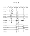
- the horizontal synchronizing signal HD is at the high level, and therefore the output of the inverter 40 is at the low level, so that the shift register 38 has been cleared.
- the horizontal synchronizing signal HD goes low at time t1
- the output of the inverter 40 goes high, so that the signal level at each of the clear terminal CLR and data input terminal A of the 2-bit shift register 38 goes high.
- a clock pulse SC is supplied at time t2
- the output (High) of the inverter 40 is loaded onto the shift register 38, so that a signal S1 at an output terminal QC of the shift register 38 goes high (Fig. 6(c)).
- the signals S1 and S2 are outputted from the output terminals QC and QD of the shift register 38, respectively, in the manner mentioned above.
- the signal S1 is fed to a first input terminal of the AND gate 46 while the signal S2 is inverted by the inverter 44 and is fed to a second input terminal of the AND gate 46.
- the signals S1 and S2 fed respectively to the first and second input terminals of the AND gate 46 goes high at time t2, so that an output signal S3 of the AND gate 46 goes high (Fig. 7(e)), and this output signal S3 of the high level is fed to one input terminal of the NAND gate 52 via the OR gate 48.
- a clock pulse SC is adapted to be supplied to another input terminal of the NAND gate 52 via the inverter 50, and a vertical synchronizing signal VD, separated from the aforesaid composite video signal, is fed to a further input terminal of the NAND gate 52.
- the vertical synchronizing signal VD is maintained at a high level throughout the operation.
- the write enable signal WE of the low level is fed from the output terminal of the NAND gate 52 to the write terminal W of the memory 56 and to a clock terminal CK of the address counter 58.
- the horizontal synchronizing signal HD is maintained at a low level, so that the counter 54 has been cleared.
- the write enable signal WE of the low level is applied to the write terminal W of the memory 56, the contents "0" of the counter 54 is loaded onto that address of the memory 56 designated by the output of the address counter 58.
- a clock pulse SC is supplied at time t3
- the contents of the address counter 58 is incremented.
- the X coordinate data outputted from the counter 54 is loaded onto the memory 56.
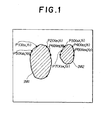
- the X coordinate data representative of the X coordinates of the level-varying points on the edges of the images shown in Fig. 1, are written into the respective addresses of the memory 56 in a manner shown in Fig. 6. Therefore, for carrying out the image processing, the position of the edge of the image is detected by reading the data from the memory 56 under the control of a computer 60. It will be appreciated that the Y coordinate of each level-varying point is detected by counting the number of zeros ("0"s) stored in the memory 56.
Landscapes
- Engineering & Computer Science (AREA)
- Multimedia (AREA)
- Physics & Mathematics (AREA)
- General Physics & Mathematics (AREA)
- Theoretical Computer Science (AREA)
- Image Analysis (AREA)
- Length Measuring Devices By Optical Means (AREA)
- Radar Systems Or Details Thereof (AREA)
Applications Claiming Priority (2)
| Application Number | Priority Date | Filing Date | Title |
|---|---|---|---|
| JP60266893A JPS62126487A (ja) | 1985-11-27 | 1985-11-27 | 2値画像のエツジ検出回路 |
| JP266893/85 | 1985-11-27 |
Publications (2)
| Publication Number | Publication Date |
|---|---|
| EP0225159A2 true EP0225159A2 (de) | 1987-06-10 |
| EP0225159A3 EP0225159A3 (de) | 1990-04-25 |
Family
ID=17437115
Family Applications (1)
| Application Number | Title | Priority Date | Filing Date |
|---|---|---|---|
| EP86309195A Withdrawn EP0225159A3 (de) | 1985-11-27 | 1986-11-25 | Bildkantendetektionssystem |
Country Status (3)
| Country | Link |
|---|---|
| US (1) | US4866783A (de) |
| EP (1) | EP0225159A3 (de) |
| JP (1) | JPS62126487A (de) |
Cited By (4)
| Publication number | Priority date | Publication date | Assignee | Title |
|---|---|---|---|---|
| FR2667177A1 (fr) * | 1990-09-21 | 1992-03-27 | Fmc Corp | Procede de compression de donnees et ensembles de traitement d'informations de bords d'objets. |
| GB2281467A (en) * | 1993-08-24 | 1995-03-01 | Roger Colston Downs | Image edge detractor and processor |
| GB2295741B (en) * | 1993-08-24 | 1998-09-09 | Downs Roger C | Topography processor system |
| US6233361B1 (en) | 1993-08-24 | 2001-05-15 | Roger Colston Downs | Topography processor system |
Families Citing this family (9)
| Publication number | Priority date | Publication date | Assignee | Title |
|---|---|---|---|---|
| JPH01173180A (ja) * | 1987-12-28 | 1989-07-07 | Stanley Electric Co Ltd | ディジタル画像における凸包の生成方法 |
| JPH0727725Y2 (ja) * | 1988-11-18 | 1995-06-21 | 富士ゼロックス株式会社 | 画像編集装置 |
| US5157486A (en) * | 1990-09-21 | 1992-10-20 | Fmc Corporation | High resolution camera sensor having a linear pixel array |
| US5460034A (en) * | 1992-07-21 | 1995-10-24 | The United States Of America As Represented By The Secretary Of The Air Force | Method for measuring and analyzing surface roughness on semiconductor laser etched facets |
| US5625709A (en) * | 1994-12-23 | 1997-04-29 | International Remote Imaging Systems, Inc. | Method and apparatus for identifying characteristics of an object in a field of view |
| US20030174864A1 (en) * | 1997-10-27 | 2003-09-18 | Digital Biometrics, Inc. | Gambling chip recognition system |
| US6636045B2 (en) * | 2001-04-03 | 2003-10-21 | Baker Hughes Incorporated | Method of determining formation anisotropy in deviated wells using separation of induction mode |
| US6985631B2 (en) * | 2002-02-20 | 2006-01-10 | Hewlett-Packard Development Company, L.P. | Systems and methods for automatically detecting a corner in a digitally captured image |
| EP1709392A1 (de) * | 2004-01-29 | 2006-10-11 | Micronic Laser Systems Ab | Verfahren zur messung der position einer markierung in einem deflektorsystem |
Family Cites Families (6)
| Publication number | Priority date | Publication date | Assignee | Title |
|---|---|---|---|---|
| US4069411A (en) * | 1969-06-23 | 1978-01-17 | Bausch & Lomb Incorporated | Image analysis system and method for minimizing paralysis angle |
| US4115805A (en) * | 1975-05-23 | 1978-09-19 | Bausch & Lomb Incorporated | Image analysis indexing apparatus and methods |
| US4115806A (en) * | 1975-05-23 | 1978-09-19 | Bausch & Lomb Incorporated | Image analysis data transfer |
| JPS573177A (en) * | 1980-06-09 | 1982-01-08 | Fujitsu Ltd | Detecting circuit for pattern change point |
| JPS6011976A (ja) * | 1983-06-30 | 1985-01-22 | Fujitsu Ltd | 画像処理装置 |
| JPS6097482A (ja) * | 1983-10-31 | 1985-05-31 | Meidensha Electric Mfg Co Ltd | パタ−ン認識装置 |
-
1985
- 1985-11-27 JP JP60266893A patent/JPS62126487A/ja active Pending
-
1986
- 1986-11-25 EP EP86309195A patent/EP0225159A3/de not_active Withdrawn
-
1988
- 1988-10-13 US US07/258,065 patent/US4866783A/en not_active Expired - Fee Related
Non-Patent Citations (2)
| Title |
|---|
| COMPUTER GRAPHICS AND IMAGE PROCESSING, vol. 17, no. 3, November 1981, pages 225-237, New York, US; G. GRANT et al.: "An efficient algorithm for boundary tracing and feature extraction" * |
| COMPUTER VISION, GRAPHICS AND IMAGE PROCESSING, vol. 28, no. 1, 28th October 1984, pages 109-125, New York, US; D.W. CAPSON: "An improved algorithm for the sequential extraction of boundaries from a raster scan" * |
Cited By (4)
| Publication number | Priority date | Publication date | Assignee | Title |
|---|---|---|---|---|
| FR2667177A1 (fr) * | 1990-09-21 | 1992-03-27 | Fmc Corp | Procede de compression de donnees et ensembles de traitement d'informations de bords d'objets. |
| GB2281467A (en) * | 1993-08-24 | 1995-03-01 | Roger Colston Downs | Image edge detractor and processor |
| GB2295741B (en) * | 1993-08-24 | 1998-09-09 | Downs Roger C | Topography processor system |
| US6233361B1 (en) | 1993-08-24 | 2001-05-15 | Roger Colston Downs | Topography processor system |
Also Published As
| Publication number | Publication date |
|---|---|
| EP0225159A3 (de) | 1990-04-25 |
| US4866783A (en) | 1989-09-12 |
| JPS62126487A (ja) | 1987-06-08 |
Similar Documents
| Publication | Publication Date | Title |
|---|---|---|
| US4866783A (en) | System for detecting edge of image | |
| US4677476A (en) | Method for detecting a movement of a television signal | |
| US4569079A (en) | Image data masking apparatus | |
| JPH03256485A (ja) | 動きベクトル検出回路 | |
| EP0454131A2 (de) | Polygonsortierungsgerät | |
| EP0562713A2 (de) | Steuerung von Signaltakt in ein digitales Signalverarbeitungssystem | |
| US4000399A (en) | Pattern counting system using line scanning | |
| US5157696A (en) | Digital signal time difference correcting circuit | |
| JP2687428B2 (ja) | 画像メモリ装置 | |
| US4581610A (en) | Method and apparatus for locally intensifying brightness in a video display device | |
| JPH0750504B2 (ja) | パタ−ン認識装置 | |
| US5023810A (en) | Image label updating device using serially connected modules | |
| RU1785017C (ru) | Устройство дл выделени контура изображени | |
| KR920000577B1 (ko) | 다중화면의 수평분할 처리회로 | |
| KR940009292B1 (ko) | 영상신호의 프레임 좌표화 및 좌표일치 펄스발생회로 | |
| SU1332311A1 (ru) | Устройство дл классификации элементов изображений | |
| JPH01296142A (ja) | 2次元画像比較検査装置 | |
| JPH0128994B2 (de) | ||
| JPH04100179A (ja) | 画像処理装置 | |
| JPS61145689A (ja) | 領域ラベリング回路 | |
| JPH05336432A (ja) | 画像の手振れ検出装置 | |
| JPS63254578A (ja) | パタ−ン認識装置 | |
| JPS62113288A (ja) | 2値画像のエツジ検出回路 | |
| JPS62108381A (ja) | 濃度ヒストグラム検出装置 | |
| JPH07193561A (ja) | フォーマット同期処理方式及び装置 |
Legal Events
| Date | Code | Title | Description |
|---|---|---|---|
| PUAI | Public reference made under article 153(3) epc to a published international application that has entered the european phase |
Free format text: ORIGINAL CODE: 0009012 |
|
| AK | Designated contracting states |
Kind code of ref document: A2 Designated state(s): DE FR GB |
|
| PUAL | Search report despatched |
Free format text: ORIGINAL CODE: 0009013 |
|
| AK | Designated contracting states |
Kind code of ref document: A3 Designated state(s): DE FR GB |
|
| 17P | Request for examination filed |
Effective date: 19901012 |
|
| 17Q | First examination report despatched |
Effective date: 19920818 |
|
| STAA | Information on the status of an ep patent application or granted ep patent |
Free format text: STATUS: THE APPLICATION IS DEEMED TO BE WITHDRAWN |
|
| 18D | Application deemed to be withdrawn |
Effective date: 19921229 |
|
| RIN1 | Information on inventor provided before grant (corrected) |
Inventor name: OHYAMA, TOSHINOBUC/O SHINKO ELECTRIC CO., LTD. |