EP0225442A2 - Entzerrte Matrixvorspannung für PROMS und EPROMS - Google Patents
Entzerrte Matrixvorspannung für PROMS und EPROMS Download PDFInfo
- Publication number
- EP0225442A2 EP0225442A2 EP86112824A EP86112824A EP0225442A2 EP 0225442 A2 EP0225442 A2 EP 0225442A2 EP 86112824 A EP86112824 A EP 86112824A EP 86112824 A EP86112824 A EP 86112824A EP 0225442 A2 EP0225442 A2 EP 0225442A2
- Authority
- EP
- European Patent Office
- Prior art keywords
- line
- voltage
- bias
- transistor
- source
- Prior art date
- Legal status (The legal status is an assumption and is not a legal conclusion. Google has not performed a legal analysis and makes no representation as to the accuracy of the status listed.)
- Granted
Links
- 230000008878 coupling Effects 0.000 claims abstract description 4
- 238000010168 coupling process Methods 0.000 claims abstract description 4
- 238000005859 coupling reaction Methods 0.000 claims abstract description 4
- 238000000034 method Methods 0.000 claims description 6
- 239000004065 semiconductor Substances 0.000 claims 2
- 230000001419 dependent effect Effects 0.000 description 4
- 230000000295 complement effect Effects 0.000 description 3
- 238000010586 diagram Methods 0.000 description 3
- 238000012986 modification Methods 0.000 description 2
- 230000004048 modification Effects 0.000 description 2
- 241000220317 Rosa Species 0.000 description 1
- 238000001514 detection method Methods 0.000 description 1
- 238000010348 incorporation Methods 0.000 description 1
Images
Classifications
-
- G—PHYSICS
- G11—INFORMATION STORAGE
- G11C—STATIC STORES
- G11C17/00—Read-only memories programmable only once; Semi-permanent stores, e.g. manually-replaceable information cards
- G11C17/14—Read-only memories programmable only once; Semi-permanent stores, e.g. manually-replaceable information cards in which contents are determined by selectively establishing, breaking or modifying connecting links by permanently altering the state of coupling elements, e.g. PROM
- G11C17/18—Auxiliary circuits, e.g. for writing into memory
-
- G—PHYSICS
- G11—INFORMATION STORAGE
- G11C—STATIC STORES
- G11C16/00—Erasable programmable read-only memories
- G11C16/02—Erasable programmable read-only memories electrically programmable
- G11C16/06—Auxiliary circuits, e.g. for writing into memory
- G11C16/24—Bit-line control circuits
Definitions
- the present invention relates to a method and apparatus for equalizing the biasing of a transistor memory cell during the READ mode across those cells which are non-selected.
- the invention is applicable to read only memory cells (ROMS), programmable read only memory cells (PROMS) and electrically programmable read only memory cells (EPROMS).
- ROMS read only memory cells
- PROMS programmable read only memory cells
- EPROMS electrically programmable read only memory cells
- a reference signal was used to drive independent bit line and array source drivers in order to condition the floating gate transistors for a READ cycle in an array of programmable and electrically programmable read only memory cells.
- the variation of the voltage level on the drain of the floating gate transistor being read due to threshold voltage or V T variations of the above-mentioned drivers rendered more uncertain the correct detection of the cell state.
- the driver of the bit line operated in a mode in which its gate voltage was not more than a V T above its drain, not only was its source voltage V T dependent, but whenever the bit line voltage rose suddenly, the latter bit line driver became non-conducting and resulted in trapping the bit line voltage in a higher than normal state.
- a bias voltage line on which there is established a voltage V BIAS is coupled to each bit line by a bit line transistor whose gate during a read mode is at least about a voltage V T above V BIAS .
- the source of each transistor is coupled to the bias voltage line by a source line transistor whose gate is more than about a voltage V T above V BIAS .
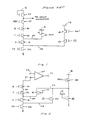
- transistors 12 are each coupled to ground through associated ground select transistors 22.
- the drain of each transistor 12 is coupled by a bit line 24 to the source-drain path of a bit transistor 14.
- the other end of the other end of the source drain path of transistor 14 is connected to a voltage V cc line 16 while its gate is fed by a reference voltage REF.
- each transistor 12 is coupled to an associated source line 28 which connects to a source-drain path of a transistor 20.
- the other end of the latter path is coupled to V cc line 16 by the source drain path of a transistor 18.
- the gate of transistor 19 is driven by the reference voltage REF while that of transistor 20 is driven by the complement VG of the voltage VG that drives the gate of ground select transistor 22.
- bit line 24 Also coupled to bit line 24 are a pair of series connected select transistors 26 and 30 driven by select lines Y and Z, respectively.
- the source-drain path of transistor 30 connects to a transistor 32 whose gate is driven by the reference voltage REF and the other end of the path being coupled to a transistor 34 connected as a load to voltage line V cc 16.
- a sense amplifier (not shown) couples to the junction of transistors 32 and 34 to measure the voltage at that point during a read cycle.
- the structure, circuit arrangement and operation of the array of memory cells of Figure 1 is similar to that set forth in U.S. Patent No. 4,314,362 issued Feb. 2, 1982 Klaas et al.
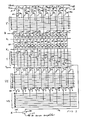
- Operation of the circuit of Figure 1 for a read mode involves selection of a particular transistor 12 by application of decode signals X, Y and Z to sets of transistors 12, 26 and 30, respectively.
- the application of reference voltage REF which is normally about 2 or 3 volts to the gate of transistor 14 causes the latter to conduct and places a voltage equal to REF -V T on bit line 24.
- the threshold voltage V T of transistor 14 is introduced as a variable on bit line 24 since transistor 14 is operating with its gate at a lower voltage than its drain (ie. 2-3 volts versus 5 volts).
- ground select transistor 22 is turned on by the application of a voltage VG to its gate thereby drawing down source line 28 close to ground.
- transistor 32 will be made conducting by voltage REF so that current will flow through it and through transistor load device 34 thereby dropping the voltage fed to the sense amplifier (not shown). Since transistor 32 also operates in a V T dependent mode its conductive state will depend on its value of V T as compared to that of transistor 14. For a V T variation of transistor 32 higher than that of transistor 14, it is possible that transistor 32 could be insufficiently conductive.
- both source line 28 and bit line 24 are coupled through transistors 20 and 14 to a V BIAS line 42.
- Line 42 is coupled through transistor 44 to V cc line 16 and through transistor 46 to ground.
- the gate of transistor 44 is connected to REF while that of transistor 46 is connected to V cc line 16.
- the gate of transistor 46 is also connected to V cc line 16 while that of transistor 20 is driven by the complement voltage of VG, designated .
- non-inverting input 60 of sense amplifier 64 is coupled directly to the drain transistor 30 while its inverting input is coupled to second reference voltage (not shown) but whose value is approximately half-way between the value on input 60 when associated transistor 12 is non-conducting and the value thereon when transistor 12 is conducting.
- decode signal X serves to select a particular row of memory cells 12, transistor 22 provides a virtual ground to a particular column of cells or transistors 12 and decode signals Y and Z connect the selected cell 12 to the sense amplifier 64.
- the presence of voltage V cc on line 16 causes transistor 14 to turn on and couple voltage V BIAS on line 42 to the bit line 24. Since voltage V cc is more than V T greater than V BIAS the full value of V BIAS will be transmitted to the bit line 24. Moreover, since all of the bit lines 24 are connected to V BIAS there is a high capacitance on line 50 which serves to stabilize it. Even though the value of V BIAS is dependent on the threshold voltage V T of transistor 44, any variation of this value of V T affects the voltage on both bit line 24 and source line 28 the same.
- the sense amplifier 64 whose non-inverting input 60 is lower than input line 62 when transistor 12 is conducting provides a low output in the latter case. If transistor 12 has been programmed so that it is nonconducting then input 60 will be higher than input 62 and output 66 will go high. The drop in voltage of bit line 24 when transistor 12 is conducting is due to the voltage drop across the channel of transistor 14 when it conducts.
- Eight lines are applied to the associated gates of 8 P-channel transistors 52 and result in a high voltage V pp being applied to respective bit lines 24 during a programming mode.
Landscapes
- Read Only Memory (AREA)
Applications Claiming Priority (2)
| Application Number | Priority Date | Filing Date | Title |
|---|---|---|---|
| US06/786,991 US4722075A (en) | 1985-10-15 | 1985-10-15 | Equalized biased array for PROMS and EPROMS |
| US786991 | 1985-10-15 |
Publications (3)
| Publication Number | Publication Date |
|---|---|
| EP0225442A2 true EP0225442A2 (de) | 1987-06-16 |
| EP0225442A3 EP0225442A3 (en) | 1989-03-08 |
| EP0225442B1 EP0225442B1 (de) | 1991-10-23 |
Family
ID=25140131
Family Applications (1)
| Application Number | Title | Priority Date | Filing Date |
|---|---|---|---|
| EP86112824A Expired EP0225442B1 (de) | 1985-10-15 | 1986-09-17 | Entzerrte Matrixvorspannung für PROMS und EPROMS |
Country Status (4)
| Country | Link |
|---|---|
| US (1) | US4722075A (de) |
| EP (1) | EP0225442B1 (de) |
| JP (1) | JPS62177796A (de) |
| DE (1) | DE3682171D1 (de) |
Cited By (2)
| Publication number | Priority date | Publication date | Assignee | Title |
|---|---|---|---|---|
| EP0432481A3 (en) * | 1989-12-14 | 1992-04-29 | Texas Instruments Incorporated | Methods and apparatus for verifying the state of a plurality of electrically programmable memory cells |
| US5208808A (en) * | 1990-09-28 | 1993-05-04 | Alcatel, N.V. | Method of assigning slots in a ucol-type star network and electronic device for carrying out such method |
Families Citing this family (7)
| Publication number | Priority date | Publication date | Assignee | Title |
|---|---|---|---|---|
| JP2513795B2 (ja) * | 1988-07-22 | 1996-07-03 | 沖電気工業株式会社 | Mos型半導体記憶装置 |
| US4903237A (en) * | 1988-08-02 | 1990-02-20 | Catalyst Semiconductor, Inc. | Differential sense amplifier circuit for high speed ROMS, and flash memory devices |
| JPH0654873B2 (ja) * | 1989-09-04 | 1994-07-20 | 株式会社東芝 | プログラマブル型論理装置 |
| US5027321A (en) * | 1989-11-21 | 1991-06-25 | Intel Corporation | Apparatus and method for improved reading/programming of virtual ground EPROM arrays |
| US5128895A (en) * | 1989-11-21 | 1992-07-07 | Intel Corporation | Method for programming a virtual ground EPROM cell including slow ramping of the column line voltage |
| US5020026A (en) * | 1989-12-14 | 1991-05-28 | Texas Instruments Incorporated | Method and apparatus for reading and programming electrically programmable memory cells |
| US5287315A (en) * | 1991-01-31 | 1994-02-15 | Texas Instruments Incorporated | Skewed reference to improve ones and zeros in EPROM arrays |
Family Cites Families (9)
| Publication number | Priority date | Publication date | Assignee | Title |
|---|---|---|---|---|
| JPS5843838B2 (ja) * | 1979-02-28 | 1983-09-29 | 富士通株式会社 | 読取り専用メモリ |
| JPS5847796B2 (ja) * | 1979-05-26 | 1983-10-25 | 富士通株式会社 | 半導体メモリ装置 |
| US4301518A (en) * | 1979-11-01 | 1981-11-17 | Texas Instruments Incorporated | Differential sensing of single ended memory array |
| US4387447A (en) * | 1980-02-04 | 1983-06-07 | Texas Instruments Incorporated | Column and ground select sequence in electrically programmable memory |
| US4314362A (en) * | 1980-02-04 | 1982-02-02 | Texas Instruments, Incorporated | Power down sequence for electrically programmable memory |
| US4344154A (en) * | 1980-02-04 | 1982-08-10 | Texas Instruments Incorporated | Programming sequence for electrically programmable memory |
| US4460981A (en) * | 1981-12-24 | 1984-07-17 | Intel Corporation | Virtual ground memory |
| JPS6095794A (ja) * | 1983-10-28 | 1985-05-29 | Hitachi Ltd | 半導体集積回路 |
| JPS60211699A (ja) * | 1984-04-06 | 1985-10-24 | Hitachi Ltd | 半導体集積回路装置 |
-
1985
- 1985-10-15 US US06/786,991 patent/US4722075A/en not_active Expired - Lifetime
-
1986
- 1986-09-17 EP EP86112824A patent/EP0225442B1/de not_active Expired
- 1986-09-17 DE DE8686112824T patent/DE3682171D1/de not_active Expired - Lifetime
- 1986-10-14 JP JP61244004A patent/JPS62177796A/ja active Pending
Cited By (2)
| Publication number | Priority date | Publication date | Assignee | Title |
|---|---|---|---|---|
| EP0432481A3 (en) * | 1989-12-14 | 1992-04-29 | Texas Instruments Incorporated | Methods and apparatus for verifying the state of a plurality of electrically programmable memory cells |
| US5208808A (en) * | 1990-09-28 | 1993-05-04 | Alcatel, N.V. | Method of assigning slots in a ucol-type star network and electronic device for carrying out such method |
Also Published As
| Publication number | Publication date |
|---|---|
| US4722075A (en) | 1988-01-26 |
| EP0225442A3 (en) | 1989-03-08 |
| DE3682171D1 (de) | 1991-11-28 |
| JPS62177796A (ja) | 1987-08-04 |
| EP0225442B1 (de) | 1991-10-23 |
Similar Documents
| Publication | Publication Date | Title |
|---|---|---|
| US5276646A (en) | High voltage generating circuit for a semiconductor memory circuit | |
| US4715014A (en) | Modified three transistor EEPROM cell | |
| EP0408037B1 (de) | Halbleiterspeicheranordnung | |
| US5218571A (en) | EPROM source bias circuit with compensation for processing characteristics | |
| US4389705A (en) | Semiconductor memory circuit with depletion data transfer transistor | |
| US4223394A (en) | Sensing amplifier for floating gate memory devices | |
| US4760555A (en) | Memory array with an array reorganizer | |
| KR100284203B1 (ko) | Eprom메모리어레이를위한스위칭그라운드를가진판독장치및방법 | |
| EP0121217B1 (de) | Ausgangspufferschaltung | |
| US4695979A (en) | Modified four transistor EEPROM cell | |
| KR930008414B1 (ko) | 비휘발성 반도체 메모리장치 | |
| US5699295A (en) | Current detection circuit for reading a memory in integrated circuit form | |
| EP0225441B1 (de) | Programmierstrom-Steuergerät | |
| KR0139101B1 (ko) | 단일 트랜지스터 메모리 셀과 함께 사용하는 고속차동 센스 증폭기 | |
| EP0576045B1 (de) | Halbleiterspeicheranordnung | |
| US4709165A (en) | Voltage supply level detecting circuit | |
| US4758748A (en) | Sense amplifier for programmable read only memory | |
| US5790466A (en) | Multiple precharging semiconductor memory device | |
| EP0225442B1 (de) | Entzerrte Matrixvorspannung für PROMS und EPROMS | |
| EP0660963B1 (de) | Hochgeschwindigkeits-speicherleseverstaerker mit reduzierung des rauschens | |
| KR100266745B1 (ko) | 멀티-비트 데이터를 저장하기 위한 반도체 메모리 장치 | |
| US6400606B1 (en) | Sense amplifier circuit for use in a nonvolatile semiconductor memory device | |
| US5038327A (en) | Decoder circuit of erasable programmable read only memory for avoiding erroneous operation caused by parasitic capacitors | |
| US5117392A (en) | Non-volatile semiconductor memory device | |
| GB2200265A (en) | Current limited epld array |
Legal Events
| Date | Code | Title | Description |
|---|---|---|---|
| PUAI | Public reference made under article 153(3) epc to a published international application that has entered the european phase |
Free format text: ORIGINAL CODE: 0009012 |
|
| AK | Designated contracting states |
Kind code of ref document: A2 Designated state(s): DE FR GB |
|
| PUAL | Search report despatched |
Free format text: ORIGINAL CODE: 0009013 |
|
| AK | Designated contracting states |
Kind code of ref document: A3 Designated state(s): DE FR GB |
|
| 17P | Request for examination filed |
Effective date: 19890721 |
|
| 17Q | First examination report despatched |
Effective date: 19901203 |
|
| GRAA | (expected) grant |
Free format text: ORIGINAL CODE: 0009210 |
|
| AK | Designated contracting states |
Kind code of ref document: B1 Designated state(s): DE FR GB |
|
| REF | Corresponds to: |
Ref document number: 3682171 Country of ref document: DE Date of ref document: 19911128 |
|
| ET | Fr: translation filed | ||
| PLBE | No opposition filed within time limit |
Free format text: ORIGINAL CODE: 0009261 |
|
| STAA | Information on the status of an ep patent application or granted ep patent |
Free format text: STATUS: NO OPPOSITION FILED WITHIN TIME LIMIT |
|
| 26N | No opposition filed | ||
| REG | Reference to a national code |
Ref country code: GB Ref legal event code: IF02 |
|
| PGFP | Annual fee paid to national office [announced via postgrant information from national office to epo] |
Ref country code: GB Payment date: 20050809 Year of fee payment: 20 |
|
| PGFP | Annual fee paid to national office [announced via postgrant information from national office to epo] |
Ref country code: FR Payment date: 20050902 Year of fee payment: 20 |
|
| PGFP | Annual fee paid to national office [announced via postgrant information from national office to epo] |
Ref country code: DE Payment date: 20050930 Year of fee payment: 20 |
|
| PG25 | Lapsed in a contracting state [announced via postgrant information from national office to epo] |
Ref country code: GB Free format text: LAPSE BECAUSE OF EXPIRATION OF PROTECTION Effective date: 20060916 |
|
| REG | Reference to a national code |
Ref country code: GB Ref legal event code: PE20 |