EP0227190B1 - Adaptive Zeileninterpolation für Anzeige mit Zeilenfolgeverfahren - Google Patents
Adaptive Zeileninterpolation für Anzeige mit Zeilenfolgeverfahren Download PDFInfo
- Publication number
- EP0227190B1 EP0227190B1 EP86202305A EP86202305A EP0227190B1 EP 0227190 B1 EP0227190 B1 EP 0227190B1 EP 86202305 A EP86202305 A EP 86202305A EP 86202305 A EP86202305 A EP 86202305A EP 0227190 B1 EP0227190 B1 EP 0227190B1
- Authority
- EP
- European Patent Office
- Prior art keywords
- line
- value
- pixel
- field
- difference
- Prior art date
- Legal status (The legal status is an assumption and is not a legal conclusion. Google has not performed a legal analysis and makes no representation as to the accuracy of the status listed.)
- Expired - Lifetime
Links
- 230000000750 progressive effect Effects 0.000 title claims description 11
- 230000003044 adaptive effect Effects 0.000 title description 3
- 230000015654 memory Effects 0.000 claims description 37
- 238000000034 method Methods 0.000 claims description 14
- 230000003111 delayed effect Effects 0.000 claims description 11
- 230000004044 response Effects 0.000 claims 2
- 238000010586 diagram Methods 0.000 description 4
- 238000001514 detection method Methods 0.000 description 3
- 238000012935 Averaging Methods 0.000 description 2
- 230000007704 transition Effects 0.000 description 2
- IJJWOSAXNHWBPR-HUBLWGQQSA-N 5-[(3as,4s,6ar)-2-oxo-1,3,3a,4,6,6a-hexahydrothieno[3,4-d]imidazol-4-yl]-n-(6-hydrazinyl-6-oxohexyl)pentanamide Chemical compound N1C(=O)N[C@@H]2[C@H](CCCCC(=O)NCCCCCC(=O)NN)SC[C@@H]21 IJJWOSAXNHWBPR-HUBLWGQQSA-N 0.000 description 1
- 230000001419 dependent effect Effects 0.000 description 1
Images


Classifications
-
- H—ELECTRICITY
- H04—ELECTRIC COMMUNICATION TECHNIQUE
- H04N—PICTORIAL COMMUNICATION, e.g. TELEVISION
- H04N7/00—Television systems
- H04N7/01—Conversion of standards, e.g. involving analogue television standards or digital television standards processed at pixel level
- H04N7/0117—Conversion of standards, e.g. involving analogue television standards or digital television standards processed at pixel level involving conversion of the spatial resolution of the incoming video signal
- H04N7/012—Conversion between an interlaced and a progressive signal
Definitions
- the invention relates to adaptive line interpolation to increase picture display quality.
- Fig. 1A As is well known, television pictures are generally generated by interlaced scanning; i.e., for each pair of fields constituting a frame, each line of the second field is positioned in space between successive lines of the first field. This is illustrated in Fig. 1A.
- Figs. 1B and 1C an edge view of the scanning lines is shown, the arrows depicting light intensity.
- the interlace pattern illustrated in Fig. 1A results in interline flicker, which becomes increasingly annoying as the size of the display is increased.
- Fig. 1B a progressive scan utilizing an adjacent line averaging algorithm is illustrated.
- a line is interpolated between two successive scan lines within each field and horizontal scanning takes place at double the interlace scan frequency.
- the problem of interline flicker has been alleviated, but, as will be noted in particular where the light intensity changes from maximum to minimum, namely at the top and bottom of the lines displayed in fig. 1B, there is smear in the vertical direction, i.e. sharp contours are destroyed.
- Fig. 1C illustrates a progressive scanning algorithm in which the interpolated lines are simply repeats of the previous line. It will be noted that the pattern is stretched in the vertical direction, while interline flicker is still present.
- Fig. 1C The algorithm of Fig. 1C is disclosed in US-A-4,415,931 which discloses an apparatus for providing a television display with doubled horizontal lines to reduce the visibility of the raster-scan structure.
- Bach incoming horizontal line of video information is stored in a memory and read twice at a double clock frequency. Each incoming horizontal line is therefore replicated.
- Each line and its delayed replica are applied to a display device scanned at double the normal rate, thereby displaying each horizontal line of information as a line pair oriented one above the other. This doubles the number of scanning lines in the display and reduces the visibility of the raster scan structure.
- EP-A-0,169,527 which counts as prior art under Art. 54(3,4) EPC for DE and GB, discloses a method of scanning line interpolation wherein when both interfield correlation and intrafield correlation are high, an intrafield average is used, while when the interfield correlation is high and the intrafield correlation is small, the pixel value from the line that yielded the high interfield correlation is copied to the new line, and when both interfield correlation and intrafield correlation are small, the pixel value from another line than the line that yielded the small interfield and intrafield correlations, is copied to the new line.
- the apparatus and method of the present invention only information from the present interlace field is used, either directly or after processing, for generating the progressive scan display. For each pixel in the line to be interpolated (new line) the pixel value immediately above and immediately below is determined, in some cases in conjunction with information (to be described later) about the corresponding pixel in the previous field. On the basis of this information, a decision is made to do one of the following things;
- step 3 above instead of using the average of pixel value from the line above and the line below, either one of the values could be picked for the "new" line.
- a memory or delay element which makes available a small number of bits for instance one bit value for each pixel in the previous field (36, Fig. 4). This one bit represents whether the previous field pixel value is above or below a first predetermined reference level.
- the values of pixels A (above) and B (below) are compared, and if the difference is above or below a second predetermined reference level a decision is made according to the following algorithm:
- the reference level is determined empirically. It should be beneath the level where the difference between b and a is sufficiently large to cause interline flicker in a normal interlace scan display.
- FIG. 2 An edge view of the scanning lines utilizing the above algorithm is illustrated in Fig. 2.
- the interlace scan lines as received are shown by solid lines or black circles, while the interpolated or "new" lines are dashed lines or white circles.
- the top line pixel in field 1 has a low pixel value
- the next solid line, line b has a high pixel value
- the difference between the amplitudes of line b and line a exceeding the reference value Under those circumstances, the pixel value of the corresponding pixel a0 in field 0 is tested. Since this value exceeds the reference level, the first "new" line pixel, namely a ⁇ , has a pixel value equal to that of pixel b.
- A value of previous field's pixel level, if above reference level, 0 if below.
- B sign of the present field's pixel level transition between the line above and line below, 1 signifying +, 0 signifying-;
- C magnitude of present field's pixel transition between line above and line below, 1 if above, 0 if below a reference level.
- F choice of upper or lower line pixel value, 1 for upper, 0 for lower.
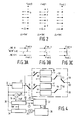
- FIG. 5 refers to an AND gate having inputs A, B and C. Its output, namely ABC is applied to the first input of an OR gate 12. The second input of OR gate 12 is applied to the output of an AND gate 14. AND gate 14 has three inputs, namely A , B , C. The output of OR gate 12 is the signal F. This, in turn, is applied to a latch 16 which is clocked by clock pulses as will now be explained with reference to Fig. 4.
- the apparatus implementing the adaptive line interpolation filter of the present invention is shown in Fig. 4. It must be kept in mind that the interlaced video input signal is assumed to have a line frequency f H , while the progressive scan output operates at a frequency 2 f H since the progressive line display includes twice the number of lines in each field.
- Terminal 20 is connected to a one line memory 22 whose output is connected to a first terminal of a selector switch 24, a first input of a scan converter 26 and the first input of a difference circuit 28.
- the second input of difference circuit 28 and a second terminal of selector switch 24 are also connected to input 20.
- Difference circuit 28 has two outputs, the first signifying the sign of the difference between the signals applied to the first and second inputs, the second corresponding to the magnitude of this difference.
- the output signifying the magnitude of the differences is applied to one input of a comparator 30 whose second input receives a reference level signal.
- the output signifying the sign of the differences is applied to the first input of a decision logic circuit 32, whose second input receives the output of comparator 30.
- the output of decision logic 32 controls the position of the selector arm of selector switch 24 as indicated by dashed lines F. Selector arm 24 is connected to the second input of scan converter 26.
- Terminal 20 is further connected to a comparator 34 whose second input also receives the reference level signal.
- the output of comparator 34 is connected through a half line delay 35 to a one bit per pixel field store 36 which exhibits a delay time equal to 262.5 TV lines for the NTSC standard.
- the output of field store 36 is connected to decision logic 32.
- Scan converter 26 includes four one-line memories 38, 40, 42 and 44.
- the first input of scan converter 26 is connected to the common terminal of a selector switch 46 whose selector arm alternately connects the input of line memory 38 and that of line memory 40 to the output of line memory 22.
- a second input of scan converter 26 is connected alternately to line memory 42 and line memory 44 in synchronism with the movement of the selector arm of switch 46 by a selector switch 48.
- the outputs of line memories 38 and 40 are connected through a selector switch 50 to a first scan terminal 52, while the outputs of line memories 42 and 44 are connected through a selector switch 54 to a second scan output terminal 56.
- the signals at terminals 56 and 52 are read out alternately at twice the line frequency by means of a selector switch 58 whose common terminal forms the output 60 of scan converter 26.
- the interlaced video input signal is applied at terminal 20. It therefore appears delayed by one line at the output of line memory 22. This is pictured in the top two lines in Fig. 6.
- the direct signal as well as the delayed signal are applied to difference circuit 28, where both the sign and the magnitude of the difference are determined.
- the reference level to which comparator 30 is set and which, in a preferred embodiment, is the same reference level as applied to comparator 34 depends upon the level which causes interline flicker in a normal interlaced display.
- the pixel values constituting the first line are applied serially to comparator 34. When a value is larger than the reference level, a "1" is stored in the corresponding location in field 36; when a value is less than the reference level, a "0" is stored.
- delay 35 causes the storing of a particular pixel to be delayed by half a line interval in addition to the standard field delay interval. This allows for the time the previous field pixel bit value is required as an input for decision logic 32.
- Switch 24 is responsive to the output of decision logic 32. Its maximum switching rate is therefore the pixel sample rate.
- Reference to Fig. 6 shows that switches 46 and 48 are operated in synchronism. Let it be assumed that the equipment is operating in the second line interval, i.e. line B is coming in. As illustrated in line 4 of Fig. 6, switches 46 and 48 are in the down position throughout this whole line interval, so that the information from line B is stored in line memory 40, while the data for the interpolated line immediately to follow line B is being stored in line memory 44.
- switches 50 and 54 are in the up position, so that read out is taking place from line memories 38 and 42.
- the data stored therein would correspond to the data of line A and of the interpolated line to follow line A, respectively.
- Switch 58 is switched in synchronism with the above-mentioned switches, but at twice the rate. (Fig. 6, Line 5).
- Line memory 38 is thus being read during the initial half of the write time interval, while the interpolated data from line memory 42 is read out during the remaining half. (Lines 8 and 9).
- the resulting output at terminal 60 is illustrated in line 12 of Fig. 6. It will be noted that compressed line data alternates with similarly compressed interpolated data.
- the output at terminal 60 after suitable processing is used to drive the display. The latter, as a result, has twice the number of lines per field as does the standard interlaced display.
Landscapes
- Engineering & Computer Science (AREA)
- Computer Graphics (AREA)
- Multimedia (AREA)
- Signal Processing (AREA)
- Television Systems (AREA)
Claims (12)
- Verfahren zum Erzeugen eines neuen Bildelementwerts für ein neues Bildelement in einer neuen Fernsehzeile, die zwischen einer ersten und einer Zweiten Zeile eines ersten Fernsehrasters das mit einem direkt vorangehenden zweiten Fernsehraster verschachtelt ist, interpoliert werden muß, dadurch gekennzeichnet, daß folgende Schritte ausgeführt werden:
Wählen eines ersten und eines zweiten Bildelements an derselben Stelle in einer Zeile über bzw. unter der neuen Fernsehzeile im ersten Raster, wobei das ersten und das zweite Bildelement einen ersten bzw. einen zweiten Bildelementwert haben,
Kombinieren des ersten und zweiten Bildelementwerts und Erzeugen eines ersten Signals als Anzeige für ihren Zusammenhang,
Wählen eines der ersten und zweiten Bildelementwerte zur Bildung des neuen Bildelementwerts abhängig vom ersten Signal. - Verfahren nach Anspruch 1, worin der Schritt des Kombinierens des ersten und zweiten Bildelementwerts den Schritt der Subtraktion des ersten vom zweiten Bildelementwert umfaßt, wobei das erste Signal ein Unterschiedssignal darstellt, das einen ersten Unterschiedswert hat, wenn der Unterschied zwischen den ersten und zweiten Bildelementwerten einen vorgegebenen Unterschied überschreitet, und einen zweiten Unterschiedswert hat, wenn der Unterschied zwischen den ersten und zweiten Bildelementwerten Kleiner ist als der vorgegebene Unterschied.
- Verfahren nach Anspruch 2, außerdem mit dem Schritt der Erzeugung eines gespeicherten Werts als Anzeige für den Wert eines entsprechend georteten Bildelements im zweiten Fernsehraster, und worin der Wählschritt das Wählen des ersten und des zweiten Bildelementwerts zur Bildung des neuen Bildelementwerts ebenfalls abhängig vom gespeicherten Wert enthält.
- Verfahren nach Anspruch 3, worin der Schritt der Erzeugung des gespeicherten Werts den Schritt des Vergleichs des Bildelementwerts des entsprechend georteten Bildelements mit einem vorgegebenen Bezugswert und der Erzeugung eines ersten und zweiten gespeicherten Werts umfaßt, wenn der entsprechende Bildelementwert dem vorgegebenen Bezugswert wenigstens gleich bzw. geringer ist.
- Verfahren nach Anspruch 4, worin der Wählschritt den Schritt zum Wählen des größeren des ersten und zweiten Bildelementwerts zur Bildung des neuen Bildelementwerts in Beantwortung des simultanen Auftretens des ersten gespeicherten Werts und des ersten Unterschiedswerts umfaßt.
- Verfahren nach Anspruch 4, worin der Wählschritt das Wählen des Kleineren der ersten und zweiten Bildelementwerte umfaßt, wenn das Unterschiedssignal den ersten Unterschiedswert hat und der gespeicherte Wert der zweite gespeicherte Wert ist.
- Apparat zum Erzeugen eines neuen Bildelementwerts für ein neues Bildelement in einer neuen Fernsehzeile, die zwischen einer ersten und einer zweiten Zeile eines ersten Fernsehrasters mit einem direkt vorangehenden zweiten Fernsehraster interpoliert werden muß, dadurch gekennzeichnet, daß folgende Elemente vorgesehen sind:
Mittel zum Erzeugen eines ersten Signals als Anzeige des Zusammenhangs zwischen dem Wert eines ersten Bildelements in einer Zeile über der neuen Fernsehzeile im ersten Raster und dem Wert eines zweiten Bildelements in einer Zeile unter der neuen Fernsehzeile im ersten Raster,
Mittel zum Erzeugen eines zweiten Signals als Anzeige des Werts eines Bildelements im zweiten Raster an einer Steile, die der Stelle des neuen Bildelements entspricht, und
Mittel zum Wählen eines Bildelementwerts aus dem ersten Bildelementwert und dem zweiten Bildelelementwert zur Bildung des neuen Bildelementwerts abhängig von den ersten und zweiten Signale. - Apparat zum Erzeugen von Zeilenfolge-Fernsehsignalen in Beantwortung empfangener Zwischenzeilen-Fernsehsignale mit einem ersten Raster, das mit einem direkt vorangehenden zweiten Raster verschachtelt ist, wobei die Zeilenfolge-Fernsehsignale interpolierte Zeilen zwischen aufeinanderfolgenden Zeilen im ersten Raster der Zwischenzeilen-Fernsehsignale aufweisen, mit Empfangsmitteln zum Empfangen der Zwischenzeilen-Fernschsignale einschl. der Horizontalzeilendaten, und gekennzeichnet durch
erste Speichermittel zum Speichern der vorangehenden Rasterbildelementwertdaten als Anzeige der Bildelementwerte im zweiten Raster,
Entscheidungslogikmittel, die mit den Empfangsmitteln zum Erzeugen von Zeileninterpolationsdaten aus den empfangenen Zeilendaten abhängig von den vorangehenden Rasterbildelementwertdaten gekoppelt sind,
eine Anzahl von Zeilenspeichermitteln,
Mittel zum Schreiben der empfangenen Zeilendaten in erste ausgewählte Zeilenspeicher der Anzahl von Zeilenspeichern und der Zeileninterpolationsdaten in zweite ausgewählte Zeilenspeicher der Anzahl von Zeilenspeichern mit einer ersten Taktfrequenz, und
Mittel zum Lesen der Zeilendaten und der Zeileninterpolationsdaten aus der Anzahl der Zeilenspeichermittel in einer vorgegebenen Sequenz und mit einer zweiten Taktfrequenz. - Apparat nach Anspruch 8, außerdem mit Verzögerungsmitteln, die mit den Empfangsmittein zum Verzögern der empfangenen Zeilendaten um ein Einzeilenintervall und gleichzeitigem Erzeugen verzögerter Zeilendaten gekoppelt sind, mit Mitteln, die mit den Empfangsmittein und den Verzögerungsmitteln zum Erzeugen eines Unterschiedssignals gekoppelt sind, das den Unterschied zwischen den verzögerten Zeilendaten und den empfangenen Zeilendaten darstellt, und mit Mitteln zum Anlegen des Unterschiedssignals an die Entscheidungslogikmittel, wobei die Entscheidungslogikmittel unter der Steuerung der vorangehenden Rasterbildelementwertdaten und eines Unterschiedsignals arbeiten.
- Apparat nach Anspruch 9, worin das Unterschiedssignal ein Größensignal als Anzeige der Größe des Unterschieds zwischen den verzögerten Zeilendaten und den empfangenen Zeilendaten sowie ein Vorzeichensignal zum Angeben des Vorzeichens des Unterschieds enthält.
- Apparat nach Anspruch 10, worin die Anzahl der Zeilenspeichermittel einen ersten, zweiten, einen dritten und einen vierten Zeilenspeicher enthält,
und worin die Schreibmittel Mittel zum Anschließen des Verzögerungsmittels abwechselnd an die ersten und die zweiten Zeilenspeicher mit der ersten vorgegebenen Horizontalzeilenfrequenz, und zwischen den dritten und den vierten Zeilenspeichermitteln, den Verzögerungsmitteln und den Empfangsmitteln angeschlossene Mittel enthalten zum selektiven Zuführen der verzögerten Zeilendaten oder der empfangenen Zeilendaten an die dritten oder vierten Zeilenspeichermittel abhängig von den Entscheidungslogikmittein. - Apparat nach Anspruch 11, worin die Schreibmittel Zeilenspeicherselektormittel zum Wählen der dritten oder vierten Zeilenspeichermittel abwechselnd synchron mit den Schreiben der verzögerten Zeilendaten in die ersten bzw. die zweiten Zeilenspeichermittel und Mittel enthalten, die mit den Zeilenspeichermitteln, den Empfangsmitteln und den Verzögerungssmittel gekoppelt sind zum selektiven Zuführen der verzögerten Zeilendaten oder der empfangenen Zeilendaten an die Zeilenspeicherselektormittel unter der Steuerung des Entscheidungslogikmittels dienen.
Applications Claiming Priority (2)
| Application Number | Priority Date | Filing Date | Title |
|---|---|---|---|
| US06/813,338 US4723163A (en) | 1985-12-26 | 1985-12-26 | Adaptive line interpolation for progressive scan displays |
| US813338 | 1991-12-23 |
Publications (3)
| Publication Number | Publication Date |
|---|---|
| EP0227190A2 EP0227190A2 (de) | 1987-07-01 |
| EP0227190A3 EP0227190A3 (en) | 1989-03-08 |
| EP0227190B1 true EP0227190B1 (de) | 1993-04-28 |
Family
ID=25212093
Family Applications (1)
| Application Number | Title | Priority Date | Filing Date |
|---|---|---|---|
| EP86202305A Expired - Lifetime EP0227190B1 (de) | 1985-12-26 | 1986-12-17 | Adaptive Zeileninterpolation für Anzeige mit Zeilenfolgeverfahren |
Country Status (6)
| Country | Link |
|---|---|
| US (1) | US4723163A (de) |
| EP (1) | EP0227190B1 (de) |
| JP (1) | JPS62159178A (de) |
| AU (1) | AU586379B2 (de) |
| CA (1) | CA1283731C (de) |
| DE (1) | DE3688368T2 (de) |
Families Citing this family (32)
| Publication number | Priority date | Publication date | Assignee | Title |
|---|---|---|---|---|
| US4896283A (en) * | 1986-03-07 | 1990-01-23 | Hewlett-Packard Company | Iterative real-time XY raster path generator for bounded areas |
| US5029001A (en) * | 1986-08-14 | 1991-07-02 | Sony Corporation | NTSC compatible TV signal transmitting system for improving vertical resolution |
| JPS6350280A (ja) * | 1986-08-20 | 1988-03-03 | Fanuc Ltd | 画像取込装置 |
| US4698675A (en) * | 1986-09-29 | 1987-10-06 | Rca Corporation | Progressive scan display system having intra-field and inter-field processing modes |
| JPH0810912B2 (ja) * | 1987-01-23 | 1996-01-31 | 株式会社日立製作所 | ス−パ−インポ−ズ装置 |
| US4816913A (en) * | 1987-11-16 | 1989-03-28 | Technology, Inc., 64 | Pixel interpolation circuitry as for a video signal processor |
| US5016193A (en) * | 1988-04-07 | 1991-05-14 | General Electric Company | Pixel and line enhancement method and apparatus |
| US4933766A (en) * | 1988-06-02 | 1990-06-12 | U.S. Philips Corporation | Interpolation filter and receiver provided with such an interpolation filter |
| NL8802365A (nl) * | 1988-09-27 | 1990-04-17 | Philips Nv | Werkwijze en schakeling voor het verwerken van een beeldsignaal. |
| US4941045A (en) * | 1988-10-11 | 1990-07-10 | Scientific-Atlanta, Inc. | Method and apparatus for improving vertical definition of a television signal by scan conversion |
| KR920004067Y1 (ko) * | 1988-12-12 | 1992-06-20 | 삼성전관 주식회사 | Id-tv의 더블 스캔회로 |
| US5126843A (en) * | 1989-03-10 | 1992-06-30 | Sony Corporation | Interpolation signal producing circuit with improved amplitude interpolation |
| JP2765012B2 (ja) * | 1989-03-10 | 1998-06-11 | ソニー株式会社 | 補間信号形成回路 |
| JPH0748838B2 (ja) * | 1989-04-27 | 1995-05-24 | 三菱電機株式会社 | テレビ画像表示装置 |
| US7382929B2 (en) | 1989-05-22 | 2008-06-03 | Pixel Instruments Corporation | Spatial scan replication circuit |
| US5424780C1 (en) * | 1989-05-22 | 2002-07-23 | James C Cooper | Apparatus and method for special scan modulation of a video display |
| US6529637B1 (en) | 1989-05-22 | 2003-03-04 | Pixel Instruments Corporation | Spatial scan replication circuit |
| JPH03258177A (ja) * | 1990-03-08 | 1991-11-18 | Sony Corp | ノンインターレース表示装置 |
| GB9005544D0 (en) * | 1990-03-12 | 1990-05-09 | Spaceward Ltd | Improved outline production from a raster image |
| US5093721A (en) * | 1990-07-10 | 1992-03-03 | Zenith Electronics Corporation | Line interpolator with preservation of diagonal resolution |
| US5182643A (en) * | 1991-02-01 | 1993-01-26 | Futscher Paul T | Flicker reduction circuit for interlaced video images |
| EP0575862B1 (de) * | 1992-06-22 | 1998-04-29 | THOMSON multimedia | Verfahren und Vorrichtung zur adaptiven Interpolation |
| DE69318216T2 (de) * | 1992-06-22 | 1998-08-27 | Thomson Multimedia Sa | Verfahren und Vorrichtung zur adaptiven Interpolation |
| JP2967014B2 (ja) * | 1993-05-24 | 1999-10-25 | キヤノン株式会社 | 画像処理装置 |
| CA2138834C (en) * | 1994-01-07 | 2004-10-19 | Robert J. Gove | Video display system with digital de-interlacing |
| KR0182930B1 (ko) * | 1996-02-17 | 1999-05-01 | 김광호 | 디스플레이 장치의 주사 방식 변환 장치 및 변환방법 |
| US5894329A (en) * | 1996-06-20 | 1999-04-13 | International Business Machines Corporation | Display control unit for converting a non-interlaced image into an interlaced image and displaying the converted image data |
| US6097837A (en) * | 1998-03-09 | 2000-08-01 | Eastman Kodak Company | Method and apparatus for removing temporal lighting variations from an image source |
| DE69920055T2 (de) * | 1999-02-26 | 2005-09-15 | Stmicroelectronics Asia Pacific Pte Ltd. | Verfahren und vorrichtung zur bestimmung von zeilensprung-/nichtzeilensprungbildern und erkennung von wiederholten halbbildern und szenenänderungen |
| JP4421722B2 (ja) * | 1999-12-14 | 2010-02-24 | シャープ株式会社 | 液晶表示装置、駆動方法及び駆動回路 |
| DE10232372B3 (de) * | 2002-07-17 | 2004-01-22 | Micronas Gmbh | Verfahren zur Interpolation eines Bildpunktes einer Zwischenzeile eines Halbbildes |
| DE102004016350A1 (de) * | 2004-04-02 | 2005-10-27 | Micronas Gmbh | Verfahren und Vorrichtung zur Interpolation eines Bildpunktes einer Zwischenzeile eines Halbbildes |
Family Cites Families (8)
| Publication number | Priority date | Publication date | Assignee | Title |
|---|---|---|---|---|
| US4322750A (en) * | 1979-05-08 | 1982-03-30 | British Broadcasting Corporation | Television display system |
| AU549207B2 (en) * | 1981-02-12 | 1986-01-16 | Sony Corporation | Double-scanning non-interlaced colour television display |
| JPS5879378A (ja) * | 1981-11-05 | 1983-05-13 | Sony Corp | テレビジヨン受像機 |
| US4415931A (en) * | 1982-03-18 | 1983-11-15 | Rca Corporation | Television display with doubled horizontal lines |
| US4484188A (en) * | 1982-04-23 | 1984-11-20 | Texas Instruments Incorporated | Graphics video resolution improvement apparatus |
| US4593315A (en) * | 1984-05-29 | 1986-06-03 | Rca Corporation | Progressive scan television receiver for non-standard signals |
| JPS6130887A (ja) * | 1984-07-23 | 1986-02-13 | Hitachi Ltd | デジタルテレビジヨン受像機の信号変換回路 |
| JPS61230584A (ja) * | 1985-04-05 | 1986-10-14 | Hitachi Ltd | 倍密走査回路 |
-
1985
- 1985-12-26 US US06/813,338 patent/US4723163A/en not_active Expired - Lifetime
-
1986
- 1986-12-17 CA CA000525632A patent/CA1283731C/en not_active Expired - Lifetime
- 1986-12-17 EP EP86202305A patent/EP0227190B1/de not_active Expired - Lifetime
- 1986-12-17 DE DE86202305T patent/DE3688368T2/de not_active Expired - Fee Related
- 1986-12-23 AU AU66903/86A patent/AU586379B2/en not_active Ceased
- 1986-12-23 JP JP61305575A patent/JPS62159178A/ja active Pending
Also Published As
| Publication number | Publication date |
|---|---|
| EP0227190A2 (de) | 1987-07-01 |
| DE3688368D1 (de) | 1993-06-03 |
| AU586379B2 (en) | 1989-07-06 |
| US4723163A (en) | 1988-02-02 |
| JPS62159178A (ja) | 1987-07-15 |
| AU6690386A (en) | 1987-07-02 |
| EP0227190A3 (en) | 1989-03-08 |
| CA1283731C (en) | 1991-04-30 |
| DE3688368T2 (de) | 1993-10-28 |
Similar Documents
| Publication | Publication Date | Title |
|---|---|---|
| EP0227190B1 (de) | Adaptive Zeileninterpolation für Anzeige mit Zeilenfolgeverfahren | |
| US5019904A (en) | Scan converter with adaptive vertical filter for single bit computer graphics systems | |
| JPH0651721A (ja) | 表示制御装置 | |
| GB2111343A (en) | Double-scanning non-interlace television receiver | |
| EP0581594B1 (de) | Anzeigesteuergerät | |
| JPH0654346A (ja) | ビデオメモリ装置 | |
| JPH01189285A (ja) | フリツカ障害抑圧装置を備えているテレビジョン受信機 | |
| US5016103A (en) | Spatial scan converter with vertical detail enhancement | |
| JPS63179685A (ja) | 順次走査変換回路 | |
| US5181110A (en) | Video signal processing circuit capable of enlarging and displaying a picture | |
| EP0394023B1 (de) | Bildwiedergabegerät | |
| JPH02246481A (ja) | ドットマトリクス表示式受像装置 | |
| JP3259628B2 (ja) | 走査線変換装置 | |
| KR0131458B1 (ko) | 비디오 화상의 재생 화질 개선 방법 및 회로 장치 | |
| JP2923966B2 (ja) | 高品位テレビジョン表示装置 | |
| EP0501462A2 (de) | Anzeigegerät | |
| KR0123769B1 (ko) | 16 : 9 화면에서의 픽쳐 인 픽쳐 표시회로 | |
| JPH0651282A (ja) | 表示制御装置 | |
| JPH10174012A (ja) | 文字表示装置 | |
| JPH0370288A (ja) | スキャンコンバータ | |
| JPS5952971A (ja) | テレビジヨン信号処理方式 | |
| JPH0651281A (ja) | 表示制御装置 | |
| JPH0686193A (ja) | マトリクス型表示装置 | |
| JPH06308900A (ja) | 表示装置 | |
| JPH0651726A (ja) | 表示制御装置 |
Legal Events
| Date | Code | Title | Description |
|---|---|---|---|
| PUAI | Public reference made under article 153(3) epc to a published international application that has entered the european phase |
Free format text: ORIGINAL CODE: 0009012 |
|
| AK | Designated contracting states |
Kind code of ref document: A2 Designated state(s): DE FR GB IT |
|
| PUAL | Search report despatched |
Free format text: ORIGINAL CODE: 0009013 |
|
| AK | Designated contracting states |
Kind code of ref document: A3 Designated state(s): DE FR GB IT |
|
| 17P | Request for examination filed |
Effective date: 19890831 |
|
| RAP1 | Party data changed (applicant data changed or rights of an application transferred) |
Owner name: NORTH AMERICAN PHILIPS CORPORATION |
|
| 17Q | First examination report despatched |
Effective date: 19911024 |
|
| GRAA | (expected) grant |
Free format text: ORIGINAL CODE: 0009210 |
|
| AK | Designated contracting states |
Kind code of ref document: B1 Designated state(s): DE FR GB IT |
|
| REF | Corresponds to: |
Ref document number: 3688368 Country of ref document: DE Date of ref document: 19930603 |
|
| ITF | It: translation for a ep patent filed | ||
| ET | Fr: translation filed | ||
| PLBE | No opposition filed within time limit |
Free format text: ORIGINAL CODE: 0009261 |
|
| STAA | Information on the status of an ep patent application or granted ep patent |
Free format text: STATUS: NO OPPOSITION FILED WITHIN TIME LIMIT |
|
| 26N | No opposition filed | ||
| ITPR | It: changes in ownership of a european patent |
Owner name: CAMBIO RAGIONE SOCIALE;PHILIPS ELECTRONICS NORTH A |
|
| REG | Reference to a national code |
Ref country code: FR Ref legal event code: CD |
|
| PGFP | Annual fee paid to national office [announced via postgrant information from national office to epo] |
Ref country code: GB Payment date: 19941130 Year of fee payment: 9 |
|
| PG25 | Lapsed in a contracting state [announced via postgrant information from national office to epo] |
Ref country code: GB Effective date: 19951217 |
|
| GBPC | Gb: european patent ceased through non-payment of renewal fee |
Effective date: 19951217 |
|
| PGFP | Annual fee paid to national office [announced via postgrant information from national office to epo] |
Ref country code: FR Payment date: 19961217 Year of fee payment: 11 |
|
| PG25 | Lapsed in a contracting state [announced via postgrant information from national office to epo] |
Ref country code: FR Free format text: THE PATENT HAS BEEN ANNULLED BY A DECISION OF A NATIONAL AUTHORITY Effective date: 19971231 |
|
| REG | Reference to a national code |
Ref country code: FR Ref legal event code: ST |
|
| PGFP | Annual fee paid to national office [announced via postgrant information from national office to epo] |
Ref country code: DE Payment date: 19990217 Year of fee payment: 13 |
|
| PG25 | Lapsed in a contracting state [announced via postgrant information from national office to epo] |
Ref country code: DE Free format text: LAPSE BECAUSE OF NON-PAYMENT OF DUE FEES Effective date: 20001003 |
|
| PG25 | Lapsed in a contracting state [announced via postgrant information from national office to epo] |
Ref country code: IT Free format text: LAPSE BECAUSE OF NON-PAYMENT OF DUE FEES Effective date: 20051217 |