EP0228624A2 - Transistor à effet de champ - Google Patents
Transistor à effet de champ Download PDFInfo
- Publication number
- EP0228624A2 EP0228624A2 EP86117164A EP86117164A EP0228624A2 EP 0228624 A2 EP0228624 A2 EP 0228624A2 EP 86117164 A EP86117164 A EP 86117164A EP 86117164 A EP86117164 A EP 86117164A EP 0228624 A2 EP0228624 A2 EP 0228624A2
- Authority
- EP
- European Patent Office
- Prior art keywords
- layer
- mixed crystal
- crystal semiconductor
- semiconductor layer
- field effect
- Prior art date
- Legal status (The legal status is an assumption and is not a legal conclusion. Google has not performed a legal analysis and makes no representation as to the accuracy of the status listed.)
- Granted
Links
Images


Classifications
-
- H—ELECTRICITY
- H10—SEMICONDUCTOR DEVICES; ELECTRIC SOLID-STATE DEVICES NOT OTHERWISE PROVIDED FOR
- H10D—INORGANIC ELECTRIC SEMICONDUCTOR DEVICES
- H10D30/00—Field-effect transistors [FET]
- H10D30/40—FETs having zero-dimensional [0D], one-dimensional [1D] or two-dimensional [2D] charge carrier gas channels
- H10D30/47—FETs having zero-dimensional [0D], one-dimensional [1D] or two-dimensional [2D] charge carrier gas channels having two-dimensional [2D] charge carrier gas channels, e.g. nanoribbon FETs or high electron mobility transistors [HEMT]
- H10D30/471—High electron mobility transistors [HEMT] or high hole mobility transistors [HHMT]
- H10D30/473—High electron mobility transistors [HEMT] or high hole mobility transistors [HHMT] having confinement of carriers by multiple heterojunctions, e.g. quantum well HEMT
- H10D30/4732—High electron mobility transistors [HEMT] or high hole mobility transistors [HHMT] having confinement of carriers by multiple heterojunctions, e.g. quantum well HEMT using Group III-V semiconductor material
-
- H—ELECTRICITY
- H10—SEMICONDUCTOR DEVICES; ELECTRIC SOLID-STATE DEVICES NOT OTHERWISE PROVIDED FOR
- H10D—INORGANIC ELECTRIC SEMICONDUCTOR DEVICES
- H10D30/00—Field-effect transistors [FET]
- H10D30/40—FETs having zero-dimensional [0D], one-dimensional [1D] or two-dimensional [2D] charge carrier gas channels
- H10D30/47—FETs having zero-dimensional [0D], one-dimensional [1D] or two-dimensional [2D] charge carrier gas channels having two-dimensional [2D] charge carrier gas channels, e.g. nanoribbon FETs or high electron mobility transistors [HEMT]
- H10D30/471—High electron mobility transistors [HEMT] or high hole mobility transistors [HHMT]
- H10D30/475—High electron mobility transistors [HEMT] or high hole mobility transistors [HHMT] having wider bandgap layer formed on top of lower bandgap active layer, e.g. undoped barrier HEMTs such as i-AlGaN/GaN HEMTs
-
- H—ELECTRICITY
- H10—SEMICONDUCTOR DEVICES; ELECTRIC SOLID-STATE DEVICES NOT OTHERWISE PROVIDED FOR
- H10D—INORGANIC ELECTRIC SEMICONDUCTOR DEVICES
- H10D84/00—Integrated devices formed in or on semiconductor substrates that comprise only semiconducting layers, e.g. on Si wafers or on GaAs-on-Si wafers
- H10D84/01—Manufacture or treatment
- H10D84/0123—Integrating together multiple components covered by H10D12/00 or H10D30/00, e.g. integrating multiple IGBTs
- H10D84/0126—Integrating together multiple components covered by H10D12/00 or H10D30/00, e.g. integrating multiple IGBTs the components including insulated gates, e.g. IGFETs
-
- H—ELECTRICITY
- H10—SEMICONDUCTOR DEVICES; ELECTRIC SOLID-STATE DEVICES NOT OTHERWISE PROVIDED FOR
- H10P—GENERIC PROCESSES OR APPARATUS FOR THE MANUFACTURE OR TREATMENT OF DEVICES COVERED BY CLASS H10
- H10P32/00—Diffusion of dopants within, into or out of wafers, substrates or parts of devices
- H10P32/10—Diffusion of dopants within, into or out of semiconductor bodies or layers
- H10P32/14—Diffusion of dopants within, into or out of semiconductor bodies or layers within a single semiconductor body or layer in a solid phase; between different semiconductor bodies or layers, both in a solid phase
- H10P32/1404—Diffusion of dopants within, into or out of semiconductor bodies or layers within a single semiconductor body or layer in a solid phase; between different semiconductor bodies or layers, both in a solid phase using predeposition followed by drive-in of impurities into the semiconductor surface, e.g. predeposition from a gaseous phase
- H10P32/1406—Diffusion of dopants within, into or out of semiconductor bodies or layers within a single semiconductor body or layer in a solid phase; between different semiconductor bodies or layers, both in a solid phase using predeposition followed by drive-in of impurities into the semiconductor surface, e.g. predeposition from a gaseous phase by ion implantation
Definitions
- the present invention relates to a field effect transistor with semiconductor hetero junction applied to a low noise amplifier circuit, a high frequency circuit, a fast logical circuit, their integrated circuits, and an integrated optics or the like.
- Fig. 1 is a cross sectional view showing a structure of a conventional field effect transistor utilizing semiconductor hetero junction, which is disclosed in, for example, an article by C.Y. Chen et all., IEEE Electron Device Letters, Vol. EDL-3, No. 6, 1982, p.152.
- a conventional field effect transistor comprises a semi-insulating indium phosphide (In P) substrate 1, an aluminum indium arsenide (Al In As) mixed crystal semiconductor layer 2 formed on the substrate 1, a gallium indium arsenide (Ga In As) mixed crystal semiconductor layer 3 formed on the mixed crystal semiconductor layer 2, an aluminum indium arsenide (Al In As) mixed crystal semiconductor layer 4 formed on the mixed crystal semiconductor layer 3, to which n-type impurities are added, a gate electrode 5 formed on the mixed crystal semiconductor layer 4, and a source electrode 6 and a drain electrode 7 provided opposed to each other on both sides of the gate electrode 5.
- a two-dimensional electron layer 8 is formed in the Ga In As mixed crystal semiconductor layer 3 and serves as a channel, so that a current path is formed between the source electrode 6 and the drain electrode 7.
- the operation of the field effect transistor is achieved by controlling voltage applied to the gate electrode 5 to modulate electron density of the two-dimensional electron layer 8 immediately under the gate electrode 5 so that the drain current is modulated.
- the Al In As mixed crystal semiconductor layer 2 is provided as a buffer layer having functions for improving the crystal property of an epitaxially grown layer (the-Ga In As mixed crystal semiconductor layer 3) formed thereon and also preventing such as diffusion of impurities from the substrate 1.
- the resistance between the two-dimensional electron layer 8 under the gate electrode 5 and the source electrode 6, that is, the source resistance is not so low and hence, various problems occur in characteristics of transistor.
- the non-negligible source resistance lowers mutual conductance, cut-off frequency and the like as well as noise figure is degraded.
- a method is developed in which impurities such as silicon and selenium are ion-implanted into the region between the source electrode 6 and the gate electrode 5 so that the resistance in the region between the source electrode 6 and the two-dimensional electron layer 8 is lowered.
- the resistance in this region is a parallel resistance formed of the Al In As mixed crystal semiconductor layers 2 and 4 and the Ga In As mixed crystal semiconductor layer 3.
- the source resistance becomes substantially equal'to the resistance of the Ga In As mixed crystal semiconductor layer 3.
- the mixed crystal semiconductor layer 3 is generally as thin as 1000 A, and if impurities more than 10 17 /cm 3 in concentration are implanted to make the layer 3 low resistance, electron mobility is rapidly reduced due to electron scattering by ionized impurities. Thus, it is difficult to effectively reduce the source resistance.
- Fig. 2 is a cross sectional view showing another structure of the conventional field effect transistor, which is also disclosed in an article by C.Y. Chen et al., IEEE Electron Device Letters, Vol. EDL-3, No.6, 1982, p. 152.
- the field effect transistor shown in Fig. 2 comprises a semi-insulating indium phosphide (In P) substrate 11, a gallium indium arsenide (Ga In As) mixed crystal semiconductor layer 12 formed on the substrate 11, a non-doped Al In As mixed crystal semiconductor layer 13 formed on the mixed crystal semiconductor layer 12, an aluminum indium arsenide (Al In As) mixed crystal semiconductor layer 14 doped with n-type impurities formed on the mixed crystal semiconductor layer 13, a gate electrode 5 formed on the mixed crystal semiconductor layer 14, and a source electrode 6 and a drain electrode 7 formed on the layer 14 and opposed to each other on respective sides of the gate electrode 5.
- the Al In As mixed crystal semiconductor layers 13 and 14 on the Ga In As mixed crystal semiconductor layer 12 comprises a wide forbidden band gap layer 19.
- the two-dimensional electron layer 8 is formed along the wide forbidden band gap layer 19 in the Ga In As mixed crystal semiconductor layer 12. Electron density in the two-dimensional electron layer 8 under the gate electrode 5 is modulated by voltage applied to the gate electrode 5 so that the drain current is modulated. As a result, the transistor operation is achieved.
- the Ga In As mixed crystal semiconductor has high electron mobility of more than 10000 cm 2 /V.sec at room temperature, so that high values of approximately 440 mS/mm at room temperature and approximately 700 mS/mm at 77°K have been obtained in the device having a gate length of 1 pm as mutual conductance indicative of the performance of the device (refer to Proceedings of 12th International Symposium on Gallium Arsenide and Related Compounds, by K. Hirose et al., entitled "700 ms/mm 2 DEGFETs fabricated from high mobility MBE-grown n-Al In As/Ga In As hetero structures", pp. 529-534.
- the source resistance can not be neglected, ⁇ o that transistor characteristics such as mutual conductance and noise figure is limited by the source resistance.
- n-type impurities are ion-implanted at least into a region to form a source resistance as described above and then, flash annealing or the like is performed to activate the implanted n-type impurities, so that the region to form a source resistance is made a low resistance.
- the rate of activated n-type impurities ion-implanted into the Al In As semiconductor layer is low, and electron mobility in the Al In As mixed crystal semiconductor layer is low such as less than 300 cm /V.sec, so that it is difficult to reduce sufficiently the resistivity of the ion-implanted Al In As mixed crystal semiconductor layer.
- the source resistance can not be sufficiently reduced, so that it is difficult to improve transistor characteristics.
- An object of the present invention is to remove the disadvantages of the conventional field effect transistor and to provide a field effect transistor having a sufficiently low source resistance and excellent characteristics of device.
- the field effect transistor according to the present invention is adapted such that in order to reduce the source resistance, an In P semiconductor layer is provided between a Ga In As mixed crystal semiconductor layer in which a two-dimensional electron layer is formed and an overlying Al In As mixed crystal semiconductor layer, or between a Ga In As mixed crystal semiconductor layer and a semi-insulating substrate, and n-type impurities are ion-implanted into at least the region to form a source resistance.
- the In P semiconductor layer is formed under the overlying Ga In As mixed crystal semiconductor layer, ion-implantation is performed to the depth reaching at least the In P layer.
- the In P semiconductor layer is formed on the underlying Ga In As mixed crystal layer, ion-implantation is performed to the depth reaching the interior of the Ga In As mixed crystal semiconductor layer.
- the rate of activation of implanted ion in the In P semiconductor layer is very high and, therefore, electron mobility of the ion-implanted In P semiconductor is higher, by more than one order, than that of the Al In As mixed crystal semiconductor.
- the source resistance can be effectively reduced, and further a gate electrode is formed on the Al In As mixed crystal semiconductor layer, so that Schottky junction at the gate electrode can be easily formed.
- the rate of activation of implanted ion of more than 60 % as well as electron mobility in an ion-implanted layer of more than 2000 cm 2 /V.sec are obtained in an In P semiconductor. Therefore, if n-type impurities of 10 14 /cm 2 are implanted, the sheet resistance of the ion-implanted layer can be less than 50 ⁇ / ⁇ in the In P semiconductor.
- the source resistance can be effectively reduced.
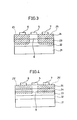
- Fig. 3 is a cross sectional view showing a structure of a field effect transistor according to an embodiment of the present invention. Referring now to Fig. 3, a manufacturing process and a structure of a field effect transistor according to an embodiment of the present invention are described.
- An In P layer 22, a Ga In As mixed crystal semiconductor layer 23, and an Al In As mixed crystal semiconductor layer 24 are formed, in this order, on an In P semi-insulating substrate 21 by using gas source molecular beam epitaxial growth or metal organic chemical vapor deposition (MOCVD). It is desirable that the In P layer 22 is an n-type doped with impurities of less than 10 15 / cm 3 or a p-type doped with impurities of less than 10 /cm in concentration and is, for example, approximately 1 ⁇ m in thickness. If ion-implantation is performed into the In P layer 22, electron mobility is 2000 cm 2 /V.sec, which is larger, by one order than that of the Al In As mixed crystal semiconductor. Therefore, even though the thickness In P layer is more than 1 ⁇ m, there occurs no problem in characteristics of device.
- MOCVD metal organic chemical vapor deposition
- the Ga In As mixed crystal semiconductor layer 23 is made to be of an n-type or a p-type having an impurity concentration of less than 10 16 /cm 3 and the thickness thereof is made to be approximately 0.1 ⁇ m. In determining an impurity concentration and a thickness of these layers, it is important that the In P semiconductor layer 22 is made to be in a depletion state when a transistor operates.
- the Al In As mixed crystal semiconductor layer 24 is made to be of an n-type having an impurity concentration of approximately 10 18 /cm 3 and 0 the thickness thereof is made to be, for example, 400 A.
- n-type impurities such as silicon having, for example, a dose of more than 10 14 /cm 2 at an acceleration voltage of more than 100 KeV are implanted by using ion implantation, whereby an ion-implanted layer reaching the In P semiconductor layer 22 is formed.
- annealing is performed, for example, for approximately ten seconds at 800°C, so that a low resistive region 25 is formed.
- the ion-implanted region is not formed in the portion underlying the region to form the gate electrode. This is achieved by, for example, forming a dummy gate on the region to form the gate electrode and performing ion-implantation utilizing the dummy gate as a mask.
- An ohmic electrode of gold-germanium alloy and the like is formed at a predetermined region on the surface of the Al In As mixed crystal semiconductor layer 24 by using evaporation and is alloyed with the mixed crystal semiconductor layer 24, so that both of a source electrode 6 and a drain electrode 7 are formed.
- a gate electrode 5 comprising platinum, gold, aluminum or the like is formed by using evaporation on the region of Al In As mixed crystal semiconductor layer 24 in which the low resistive layer 25 is not formed, so that a field effect transistor is completed.
- impurity ions are implanted at a high acceleration voltage, impurities can be distributed mainly within the In P layer 22, and the source resistance can be reduced while maintaining a low impurity concentration in the neighborhood of the gate electrode 5. It is important to maintain a low impurity concentration in the neighborhood of the gate electrode 5 to raise the breakdown voltage of the gate in the transistor. Thus, transistor characteristics can be improved without decreasing the breakdown voltage of the gate in a manner of the above described embodiment.
- Fig. 4 is a cross sectional view showing a structure of a field effect transistor according to another embodiment of the present invention. Referring now to Fig. 4, a manufacturing process and a structure of the field effect transistor comprising a wide forbidden band gap layer according to another embodiment of the present invention are described.
- An Al In As mixed crystal semiconductor layer 32 serving as a buffer layer is formed on the In P semi-insulating substrate 21 by using metal organic chemical vapor deposition (MOCVD) or gas source molecular beam epitaxial growth and then, the Ga In As mixed crystal semiconductor layer 23, an In P layer 34, and the Al In As mixed crystal semiconductor layer 24 are formed by using the same process.
- the In P layer 34 and the Al In As mixed crystal semiconductor layer 24 form a wide forbidden band gap layer 39.
- the rate of activation of implanted ions is high and the sheet resistance thereof can be made smaller, by more than one order, than that of the Al In As mixed semiconductor, so that it is found effective from the viewpoint of reducing the source resistance to utilize the In P semiconductor layer as a wide forbidden band gap layer.
- the wide forbidden band gap layer comprises only the In P semiconductor layer, various problems as described below occur. More specifically, in the field effect transistor with such a structure as shown, the gate electrode 5 must form Schottky junction with a wide forbidden band gap layer 39. However, it is generally difficult to form Schottky junction with the In P semiconductor.
- the Al In As mixed crystal semiconductor layer 24 with which Schottky junction can be easily formed is provided on the surface of the In P layer 34 to make the wide forbidden band gap layer 39 a multi-layer structure, so that effective reduction of the source resistance and excellent gate characteristics (formation of stable Schottky junction) are achieved.
- the Al In As mixed crystal semiconductor layer 32 serving as a buffer layer is provided for improving the crystal property of the epitaxial growth layer formed thereon and preventing such as diffusion of impurities from the semi-insulating substrate 21.
- the Al In As mixed crystal semiconductor layer 32 may not be provided, depending on characteristics or the like required for a transistor.
- each layer 32, 23, 34, 24 differs depending on the designed value of the threshold voltage of a transistor or the like.
- the Al In As mixed crystal semiconductor layer 32 serving as a buffer layer is approximately 0.5 ⁇ m thick
- the Ga In As mixed crystal semiconductor layer 23 is approximately 20 nm to 200 nm thick
- the In P layer 34 is approximately 10 nm to 30 nm thick
- the Al In As mixed crystal semiconductor layer 24 is approximately 10 nm in thickness.
- the amount of impurities added to each layer before formation of a low resistive layer also differs depending on the designed value of the threshold voltage or the like.
- n-type impurities of approximately 2 x 10 18 /cm 3 are added to the In P layer 34.
- the region in the range of approximately 10 nm from the surface on the side of the Ga In As mixed crystal semiconductor layer 23 in the In P layer 34 may be a non-doped region for preventing the hetero junction interface from being damaged (deteriorated).
- n-type impurities such as silicon and selenium are ion-implanted into the region except for the region to form the gate electrode under the condition of an acceleration voltage of more than 100 KeV and a dose of more than 10 14 /cm 2 .
- annealing is performed at 800°C for ten seconds, so that a low resistive region 25' comprising an ion-implanted layer reaching the interior of the Ga In As mixed crystal semiconductor layer 23 is formed.
- An ohmic electrode of gold, germanium or the like is formed in a predetermined region on the surface of the Al In As mixed crystal semiconductor layer 24 and then, ohmic electrode is alloyed with the underlying mixed crystal semiconductor layer 24, so the source electrode 6 and the drain electrode 7 are formed.
- the gate electrode 5 comprising aluminum, platinum, tungsten, silicide or the like is formed on the surface of the region in which the low resistive region 25' between the source electrode 6 and the drain electrode 7 is formed, by using evaporation or the like, whereby the field effect transistor is completed.
- the low resistive region 25' obtained by ion-implantation of n-type impurities does not overlap with the gate electrode 5 for the purpose of reducing parasitic capacitance and improving the reverse direction breakdown voltage.
- Fig. 5 is a cross sectional view showing a structure of the field effect transistor according to another embodiment of the present invention.
- the low resistive region 25' obtained by ion-implantation of n-type impurities does not overlap with the gate electrode 5. If the accuracy of mask alignment of the photolithography technique in the - transistor manufacturing process is satisfactory, the overlapping region can be surely removed without any difficulty. However, if the accuracy of mask alignment of the photolithography technique is not satisfactory and reproducability of transistor characteristics is not so sufficient, it becomes necessary to use the self-alignment technique utilizing a refractory gate or a dummy gate.
- the refractory gate or a dummy gate each having a size slightly larger than that of gate electrode 5 is formed in the region to form the gate electrode 5, and ion-implantation is performed utilizing the gate as a mask in a self-alignment manner, so that the overlap of the gate electrode 5 with the low resistive region 25' can be surely removed.
- the field effect transistor with a structure shown in Figs. 4 and 5 can effectively reduce the source resistance, so that a field effect transistor having high mutual conductance and low noise can be obtained.
- Fig. 6 is a cross sectional view showing a structure according to another embodiment of the present invention.
- the field effect transistor shown in Fig. 6 comprises an Al In As mixed crystal semiconductor layer 40 provided between the Ga In As mixed crystal semiconductor layer 23 and the In P semiconductor layer 34 in order to enhance the quantum mechanical enclosing effect of two-dimensional electron to be a channel. It is desirable that the Al In As mixed crystal semiconductor layer 40 is 50-100 A in thickness and includes non-doped impurities.
- an In P mixed crystal layer to be low resistance is provided in a region to form a source resistance by ion-implantation of impurities, and a low resistive region is formed at least in the region to form a source resistance by ion implantation, so that the source resistance can be effectively reduced and a field effect transistor having high mutual conductance and low noise figure can be achieved.
- a large contribution is made to the application field such as a low noise amplifier circuit, a fast logical circuit, integrated circuits thereof, or an integrated optics.
Landscapes
- Junction Field-Effect Transistors (AREA)
Applications Claiming Priority (4)
| Application Number | Priority Date | Filing Date | Title |
|---|---|---|---|
| JP286747/85 | 1985-12-19 | ||
| JP60286747A JPS62145779A (ja) | 1985-12-19 | 1985-12-19 | 電界効果トランジスタ |
| JP61017571A JPS62174976A (ja) | 1986-01-28 | 1986-01-28 | 電界効果トランジスタ |
| JP17571/86 | 1986-01-28 |
Publications (3)
| Publication Number | Publication Date |
|---|---|
| EP0228624A2 true EP0228624A2 (fr) | 1987-07-15 |
| EP0228624A3 EP0228624A3 (en) | 1989-10-18 |
| EP0228624B1 EP0228624B1 (fr) | 1993-04-21 |
Family
ID=26354120
Family Applications (1)
| Application Number | Title | Priority Date | Filing Date |
|---|---|---|---|
| EP86117164A Expired - Lifetime EP0228624B1 (fr) | 1985-12-19 | 1986-12-09 | Transistor à effet de champ |
Country Status (5)
| Country | Link |
|---|---|
| US (1) | US4764796A (fr) |
| EP (1) | EP0228624B1 (fr) |
| KR (1) | KR900000073B1 (fr) |
| CA (1) | CA1247755A (fr) |
| DE (1) | DE3688318T2 (fr) |
Cited By (2)
| Publication number | Priority date | Publication date | Assignee | Title |
|---|---|---|---|---|
| EP0482726A3 (en) * | 1990-10-26 | 1993-07-21 | Nippon Telegraph And Telephone Corporation | Heterojunction field-effect transistor |
| US5449928A (en) * | 1992-10-27 | 1995-09-12 | Nippondenso Co., Ltd. | Compound semiconductor substrate having a hetero-junction and a field-effect transistor using the same |
Families Citing this family (8)
| Publication number | Priority date | Publication date | Assignee | Title |
|---|---|---|---|---|
| JPS63276267A (ja) * | 1987-05-08 | 1988-11-14 | Fujitsu Ltd | 半導体装置の製造方法 |
| JP2630445B2 (ja) * | 1988-10-08 | 1997-07-16 | 富士通株式会社 | 半導体装置 |
| JP2873583B2 (ja) * | 1989-05-10 | 1999-03-24 | 富士通株式会社 | 高速半導体装置 |
| JP2919581B2 (ja) * | 1990-08-31 | 1999-07-12 | 三洋電機株式会社 | 速度変調トランジスタ |
| JP2786327B2 (ja) * | 1990-10-25 | 1998-08-13 | 三菱電機株式会社 | ヘテロ接合電界効果トランジスタ |
| JPH04184973A (ja) * | 1990-11-19 | 1992-07-01 | Mitsubishi Electric Corp | 長波長光送信oeic |
| JP4186032B2 (ja) * | 2000-06-29 | 2008-11-26 | 日本電気株式会社 | 半導体装置 |
| US20050116290A1 (en) * | 2003-12-02 | 2005-06-02 | De Souza Joel P. | Planar substrate with selected semiconductor crystal orientations formed by localized amorphization and recrystallization of stacked template layers |
Family Cites Families (4)
| Publication number | Priority date | Publication date | Assignee | Title |
|---|---|---|---|---|
| JPS54124991A (en) * | 1978-03-23 | 1979-09-28 | Fujitsu Ltd | Semiconductor luminous unit |
| JPS58196057A (ja) * | 1982-05-11 | 1983-11-15 | Fujitsu Ltd | 半導体装置 |
| JPS59100576A (ja) * | 1982-11-30 | 1984-06-09 | Fujitsu Ltd | 半導体装置 |
| JPS60140874A (ja) * | 1983-12-28 | 1985-07-25 | Hitachi Ltd | 半導体装置 |
-
1986
- 1986-12-09 DE DE8686117164T patent/DE3688318T2/de not_active Expired - Fee Related
- 1986-12-09 US US06/939,716 patent/US4764796A/en not_active Expired - Lifetime
- 1986-12-09 EP EP86117164A patent/EP0228624B1/fr not_active Expired - Lifetime
- 1986-12-17 CA CA000525579A patent/CA1247755A/fr not_active Expired
- 1986-12-17 KR KR1019860010809A patent/KR900000073B1/ko not_active Expired
Cited By (2)
| Publication number | Priority date | Publication date | Assignee | Title |
|---|---|---|---|---|
| EP0482726A3 (en) * | 1990-10-26 | 1993-07-21 | Nippon Telegraph And Telephone Corporation | Heterojunction field-effect transistor |
| US5449928A (en) * | 1992-10-27 | 1995-09-12 | Nippondenso Co., Ltd. | Compound semiconductor substrate having a hetero-junction and a field-effect transistor using the same |
Also Published As
| Publication number | Publication date |
|---|---|
| US4764796A (en) | 1988-08-16 |
| DE3688318T2 (de) | 1993-07-29 |
| KR870006679A (ko) | 1987-07-13 |
| KR900000073B1 (ko) | 1990-01-19 |
| EP0228624A3 (en) | 1989-10-18 |
| EP0228624B1 (fr) | 1993-04-21 |
| CA1247755A (fr) | 1988-12-28 |
| DE3688318D1 (de) | 1993-05-27 |
Similar Documents
| Publication | Publication Date | Title |
|---|---|---|
| US5701019A (en) | Semiconductor device having first and second stacked semiconductor layers, with electrical contact to the first semiconductor layer | |
| EP0181091B1 (fr) | Transistor à effet de champ à grille Schottky et méthode de fabrication pour cela | |
| US5093275A (en) | Method for forming hot-carrier suppressed sub-micron MISFET device | |
| US5012306A (en) | Hot-carrier suppressed sub-micron MISFET device | |
| EP0487220A2 (fr) | Transistor à effet de champ du type SOI et procédé pour sa fabrication | |
| GB2285175A (en) | High electron mobility transistor | |
| KR920003799B1 (ko) | 반도체 장치 | |
| KR930002320B1 (ko) | 반도체 장치 및 그의 제조 방법 | |
| US4764796A (en) | Heterojunction field effect transistor with two-dimensional electron layer | |
| EP0201873A2 (fr) | Procédé de fabrication d'un transistor à effet de champ métal-semi-conducteur et transistor ainsi obtenu | |
| US5949095A (en) | Enhancement type MESFET | |
| US4783688A (en) | Schottky barrier field effect transistors | |
| JPH0259624B2 (fr) | ||
| US5493136A (en) | Field effect transistor and method of manufacturing the same | |
| JPH0324782B2 (fr) | ||
| US4486766A (en) | Schottky barrier field effect transistors | |
| US4771324A (en) | Heterojunction field effect device having an implanted region within a device channel | |
| US5532507A (en) | MES field effect transistor possessing lightly doped drain | |
| EP0317345B1 (fr) | Transistor à effet de champ | |
| EP0723300A2 (fr) | Dispositif semi-conducteur avec électrode de Schattky | |
| US5107314A (en) | Gallium antimonide field-effect transistor | |
| KR910006698B1 (ko) | 반도체 장치 | |
| EP0283878A1 (fr) | Transistor à effet de champ | |
| JPH07142508A (ja) | 電界効果型素子とその製造方法 | |
| JP3034546B2 (ja) | 電界効果型トランジスタの製造方法 |
Legal Events
| Date | Code | Title | Description |
|---|---|---|---|
| PUAI | Public reference made under article 153(3) epc to a published international application that has entered the european phase |
Free format text: ORIGINAL CODE: 0009012 |
|
| AK | Designated contracting states |
Kind code of ref document: A2 Designated state(s): DE FR GB IT |
|
| RAP1 | Party data changed (applicant data changed or rights of an application transferred) |
Owner name: SUMITOMO ELECTRIC INDUSTRIES, LIMITED |
|
| PUAL | Search report despatched |
Free format text: ORIGINAL CODE: 0009013 |
|
| AK | Designated contracting states |
Kind code of ref document: A3 Designated state(s): DE FR GB IT |
|
| RHK1 | Main classification (correction) |
Ipc: H01L 29/76 |
|
| 17P | Request for examination filed |
Effective date: 19891012 |
|
| 17Q | First examination report despatched |
Effective date: 19910228 |
|
| GRAA | (expected) grant |
Free format text: ORIGINAL CODE: 0009210 |
|
| AK | Designated contracting states |
Kind code of ref document: B1 Designated state(s): DE FR GB IT |
|
| REF | Corresponds to: |
Ref document number: 3688318 Country of ref document: DE Date of ref document: 19930527 |
|
| ITF | It: translation for a ep patent filed | ||
| ET | Fr: translation filed | ||
| PLBE | No opposition filed within time limit |
Free format text: ORIGINAL CODE: 0009261 |
|
| STAA | Information on the status of an ep patent application or granted ep patent |
Free format text: STATUS: NO OPPOSITION FILED WITHIN TIME LIMIT |
|
| 26N | No opposition filed | ||
| PGFP | Annual fee paid to national office [announced via postgrant information from national office to epo] |
Ref country code: GB Payment date: 19951130 Year of fee payment: 10 |
|
| PGFP | Annual fee paid to national office [announced via postgrant information from national office to epo] |
Ref country code: FR Payment date: 19951212 Year of fee payment: 10 |
|
| PGFP | Annual fee paid to national office [announced via postgrant information from national office to epo] |
Ref country code: DE Payment date: 19951214 Year of fee payment: 10 |
|
| PG25 | Lapsed in a contracting state [announced via postgrant information from national office to epo] |
Ref country code: GB Effective date: 19961209 |
|
| GBPC | Gb: european patent ceased through non-payment of renewal fee |
Effective date: 19961209 |
|
| PG25 | Lapsed in a contracting state [announced via postgrant information from national office to epo] |
Ref country code: FR Effective date: 19970829 |
|
| PG25 | Lapsed in a contracting state [announced via postgrant information from national office to epo] |
Ref country code: DE Effective date: 19970902 |
|
| REG | Reference to a national code |
Ref country code: FR Ref legal event code: ST |
|
| PG25 | Lapsed in a contracting state [announced via postgrant information from national office to epo] |
Ref country code: IT Free format text: LAPSE BECAUSE OF NON-PAYMENT OF DUE FEES;WARNING: LAPSES OF ITALIAN PATENTS WITH EFFECTIVE DATE BEFORE 2007 MAY HAVE OCCURRED AT ANY TIME BEFORE 2007. THE CORRECT EFFECTIVE DATE MAY BE DIFFERENT FROM THE ONE RECORDED. Effective date: 20051209 |