EP0229656A2 - Méthode de commande pour onduleurs à modulation de largeur d'impulsion - Google Patents
Méthode de commande pour onduleurs à modulation de largeur d'impulsion Download PDFInfo
- Publication number
- EP0229656A2 EP0229656A2 EP87100325A EP87100325A EP0229656A2 EP 0229656 A2 EP0229656 A2 EP 0229656A2 EP 87100325 A EP87100325 A EP 87100325A EP 87100325 A EP87100325 A EP 87100325A EP 0229656 A2 EP0229656 A2 EP 0229656A2
- Authority
- EP
- European Patent Office
- Prior art keywords
- voltage
- output
- pulse mode
- pulse
- inverter
- Prior art date
- Legal status (The legal status is an assumption and is not a legal conclusion. Google has not performed a legal analysis and makes no representation as to the accuracy of the status listed.)
- Granted
Links
- 238000000034 method Methods 0.000 title description 6
- 230000008033 biological extinction Effects 0.000 claims description 7
- 230000007423 decrease Effects 0.000 claims description 4
- 230000015654 memory Effects 0.000 claims description 2
- 230000008859 change Effects 0.000 description 13
- 230000006698 induction Effects 0.000 description 6
- 238000010586 diagram Methods 0.000 description 5
- 230000000694 effects Effects 0.000 description 4
- 238000010276 construction Methods 0.000 description 3
- 230000003247 decreasing effect Effects 0.000 description 3
- 101100524639 Toxoplasma gondii ROM3 gene Proteins 0.000 description 2
- 230000004048 modification Effects 0.000 description 2
- 238000012986 modification Methods 0.000 description 2
- 101150065817 ROM2 gene Proteins 0.000 description 1
- 101100524644 Toxoplasma gondii ROM4 gene Proteins 0.000 description 1
- 230000006870 function Effects 0.000 description 1
- 230000009467 reduction Effects 0.000 description 1
- 230000001172 regenerating effect Effects 0.000 description 1
- 230000004044 response Effects 0.000 description 1
Images


Classifications
-
- H—ELECTRICITY
- H02—GENERATION; CONVERSION OR DISTRIBUTION OF ELECTRIC POWER
- H02P—CONTROL OR REGULATION OF ELECTRIC MOTORS, ELECTRIC GENERATORS OR DYNAMO-ELECTRIC CONVERTERS; CONTROLLING TRANSFORMERS, REACTORS OR CHOKE COILS
- H02P27/00—Arrangements or methods for the control of AC motors characterised by the kind of supply voltage
- H02P27/04—Arrangements or methods for the control of AC motors characterised by the kind of supply voltage using variable-frequency supply voltage, e.g. inverter or converter supply voltage
- H02P27/06—Arrangements or methods for the control of AC motors characterised by the kind of supply voltage using variable-frequency supply voltage, e.g. inverter or converter supply voltage using DC to AC converters or inverters
- H02P27/08—Arrangements or methods for the control of AC motors characterised by the kind of supply voltage using variable-frequency supply voltage, e.g. inverter or converter supply voltage using DC to AC converters or inverters with pulse width modulation
-
- H—ELECTRICITY
- H02—GENERATION; CONVERSION OR DISTRIBUTION OF ELECTRIC POWER
- H02M—APPARATUS FOR CONVERSION BETWEEN AC AND AC, BETWEEN AC AND DC, OR BETWEEN DC AND DC, AND FOR USE WITH MAINS OR SIMILAR POWER SUPPLY SYSTEMS; CONVERSION OF DC OR AC INPUT POWER INTO SURGE OUTPUT POWER; CONTROL OR REGULATION THEREOF
- H02M7/00—Conversion of AC power input into DC power output; Conversion of DC power input into AC power output
- H02M7/42—Conversion of DC power input into AC power output without possibility of reversal
- H02M7/44—Conversion of DC power input into AC power output without possibility of reversal by static converters
- H02M7/48—Conversion of DC power input into AC power output without possibility of reversal by static converters using discharge tubes with control electrode or semiconductor devices with control electrode
- H02M7/53—Conversion of DC power input into AC power output without possibility of reversal by static converters using discharge tubes with control electrode or semiconductor devices with control electrode using devices of a triode or transistor type requiring continuous application of a control signal
- H02M7/537—Conversion of DC power input into AC power output without possibility of reversal by static converters using discharge tubes with control electrode or semiconductor devices with control electrode using devices of a triode or transistor type requiring continuous application of a control signal using semiconductor devices only, e.g. single switched pulse inverters
- H02M7/5387—Conversion of DC power input into AC power output without possibility of reversal by static converters using discharge tubes with control electrode or semiconductor devices with control electrode using devices of a triode or transistor type requiring continuous application of a control signal using semiconductor devices only, e.g. single switched pulse inverters in a bridge configuration
- H02M7/53871—Conversion of DC power input into AC power output without possibility of reversal by static converters using discharge tubes with control electrode or semiconductor devices with control electrode using devices of a triode or transistor type requiring continuous application of a control signal using semiconductor devices only, e.g. single switched pulse inverters in a bridge configuration with automatic control of output voltage or current
- H02M7/53873—Conversion of DC power input into AC power output without possibility of reversal by static converters using discharge tubes with control electrode or semiconductor devices with control electrode using devices of a triode or transistor type requiring continuous application of a control signal using semiconductor devices only, e.g. single switched pulse inverters in a bridge configuration with automatic control of output voltage or current with digital control
Definitions
- the present invention relates to a control apparatus for a pulse width modulation inverter, and more particularly to a control apparatus having an improved changeover function between a three pulse mode and a single pulse mode of an inverter output voltage.
- a pulse width modulation inverter (called a PWM inverter, hereinafter)
- the number of voltage pulses in the half cycle of the operation period of the PWM inverter is varied during the control of the output AC voltage thereof.
- the number of the output voltage pulses in the half cycle of the operation period of the inverter must be changed over from three pulses to one pulse in order to obtain the highest output voltage possible, that is, the operation of the inverter has to be switched from a three pulse mode to a single pulse mode.
- a control system is intended to solve the following problems in an adjustable voltage/adjustable frequency PWM inverter, i.e., the undesirable change in the inverter output voltage upon changeover between a three pulse mode and a single pulse mode, and the phase deviation of the fundamental component of the inverter output voltage at that time.
- This control system is not yet devoid of problems that the control is complicated and the phase of the fundamental component of the inverter output voltage still changes during the course of the phase control which is conducted with three pulses for the changeover from the three pulse mode to the single pulse mode and vice versa.
- Japanese Patent Laid-open No.57-85583 there is disclosed a control method of obtaining gate signals of a PWM inverter by comparison of a triangular wave as a carrier wave and two sinusoidal waves as modulating waves which have the phase difference of l20° from each other. Also in this method, however, the phase deviation occurs in the fundamental component of the inverter output voltage at the time of changeover between a three pulse mode and a single pulse mode. Further, in this method, it is very difficult due to the inductance of a motor supplied by the inverter that the inverter output voltage in the single pulse mode is determined in advance to be almost equal to the maximal inverter output voltage in the three pulse mode, and therefore the undesirable change in the inverter output voltage can not be suppressed.
- Japanese Patent Publication No.60-24670 discloses a method of generating a multipulse current in every half cycle of the fundamental component of the output current in a current source inverter.
- this prior art only concerns the reduction of higher harmonic components included in the output current and does not disclose that the number of current pulses is changed over for controlling the output current of the inverter. Therefore, although the waveform of gate signals similar to those according to the present invention is shown, there is nowhere in the prior art the description of the change in the output voltage cr current and the phase deviation which occur at the time of changeover between a three pulse mode and a single pulse mode of the output voltage or current of an PWM inverter.
- a feature of the present invention is in that, in a PWM inverter, in which the number of pulses of a line voltage (called line voltage pulses, hereinafter) for every half cycle of an output AC voltage of the inverter is changed over in accordance with the frequency of the output AC voltage and the intervals between the line voltage pulses are controlled in every mode of the respective numbers of the line voltage pulses, a first three pulse mode, in which three line voltage pulses exist within l20° in the electric angle of the output AC voltage, is changed over to a single pulse mode, in which the width of the line voltage pulse is equal to l20° in the same electric angle, through a second three pulse mode, which is composed of two line voltage pulses positioned on both sides outside the period of l20° in the same electric angle and a center line voltage pulse positioned between the two line voltage pulses.
- a first three pulse mode in which three line voltage pulses exist within l20° in the electric angle of the output AC voltage
- a single pulse mode in which the width of the line
- the maximal output AC voltage in the second three pulse mode can be made substantially equal to that in the single pulse mode by suitably controlling the pulse width of the two line voltage pulses on both sides and the intervals between the center line voltage pulse and the two line voltage pulses, so that the jump of the output AC voltage and the phase deviation in the output AC voltage, which have occurred in the conventional apparatus upon changeover between the three pulse mode and the single pulse mode, can be prevented.
- Fig. l is a block diagram showing the general construction of a control apparatus for a PWM inverter according to an embodiment of the present invention, which is applied to the control of an induction motor;
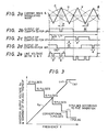
- Figs. 2a to 2e are drawings for explaining the generation of gate signals for the inverter and the waveform of a line voltage of an output AC voltage of the inverter in a first three pulse mode;
- Fig. 3 is a diagram showing the relation of the number of line voltage pulses and the output AC voltage with respect to the frequency of the output AC voltage;
- Figs. 4a to 4f show the relation between the gate signals and the line voltage in the first three pulse mode when the intervals between the line voltage pulses are minimal, and that in the single pulse mode;
- Figs. 5a to 5g are drawings for explaining the generation of gate signals for the inverter and the waveform of the line voltage of the output AC voltage in a second three pulse mode;
- Figs. 6a to 6f show the relation between the gate signals and the line voltage in the second three pulse mode when the intervals between the line voltage pulses are minimal, and that in the single pulse mode;
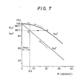
- Fig. 7 shows the characteristics of the inverter output voltage with respect to the interval between the line voltage pulses in the first and the second three pulse modes
- Fig. 8 is a block diagram showing the detailed arrangement of modulation means utilized in the control apparatus shown in Fig. l;
- Figs. 9a to 9l are drawings for explaining the generation of gate signals for the inverter by the modulation means shown in Fig. 8;
- Figs. l0a to l0d are drawings for explaining a modification of the generation of the gate signals for the inverter.
- Figs. lla to lld are drawings for explaining another modification of the generation of the gate signals for the inverter.
- Fig. l is a schematic diagram showing a general construction of a control apparatus for a PWM inverter, applied to an induction motor control, in accordance with an embodiment of the present invention.
- Reference numeral l represents a DC power source, 2 a pulse width modulation inverter consisting of control switching devices UP, VP, WP and UN, VN, WN such as thyristors, 3 an induction motor and 5 a modulation circuit consisting of carrier wave generation means 5l, modulation wave generation means 52, comparison means 53 and control means 54.
- the control switching devices UP to WN of the inverter 2 are turned on or off in a predetermined sequence by the output of this modulation circuit 5 through a gate controller 4.
- the rotation frequency f n of the induction motor 3 is detected by an f n detector 6, and a slip frequency f s is added to, and subtracted from, the rotation frequency f n by an adder l0 during power running and regenerative running, respectively.
- This becomes an output frequency f ( f n ⁇ f s ) of the inverter 2.
- the slip frequency f s is controlled by an f s controller 9 by detecting a value I M of the current of the induction motor 3 by a current detector 7 and comparing the detected value I M with a current command I p in a comparator 8.
- the modulation circuit 5 receives the output of the adder l0.
- a first carrier wave generator 5ll of the carrier wave generation means 5l generates an alternating triangular wave C as shown in Fig. 2a
- a sinusoidal modulation wave generator 52l of the modulation wave generation means 52 generates sinusoidal modulating waves for U, V and W phases as shown by U, V and W in Fig. 2a.
- the comparison means 53 compares the sinusoidal modulating waves U, V and W with the triangular carrier wave C and generates gate pulses for the control switching devices UP, VP and WP, as shown in Figs. 2b to 2d.
- Pulses obtained by inversing the pulses shown in these figures are made gate pulses for the control switching devices UN, VN and WN. Although the detailed explanation is omitted here, the line voltage between two phases of the inverter output voltage has the waveform obtained by the exclusive-OR of the gate pulses of the corresponding phases. Therefore, the line voltage between phases U and V of the inverter 2 exhibits the waveform shown in Fig. 2e.
- Fig. 2 there is shown an example, in which three pulses exist in the half cycle of the output voltage of the inverter 2.
- This mode is conventional and called a first three pulse mode hereinafter.
- the number of pulses of the output voltage of the inverter 2 contained in every half cycle thereof is controlled by changing the ratio of the frequency of the triangular carrier wave C to that of the sinusoidal modulating waves U, V and W; usually the frequency of the carrier wave is changed, and that of the modulating wave is maintained constant.
- This pulse number is changed in the order of 27, l5, 9, 5 and 3 pulses, for example, as shown in Fig. 3, by the control means 54 with respect to the output frequency f of the inverter 2.
- the output voltage V M of the inverter 2 is controlled by varying the width ⁇ of a slit in the gate pulses as shown in Figs. 2b to 2d and therefore in the line voltage as shown in Fig. 2e.
- the width ⁇ of the slit can be controlled by varying the modulation factor V C , i.e., the ratio of the peak value of the sinusoidal modulating waves U, V and W to that of the triangular carrier wave C, by a modulation factor calculator ll, in such a manner that the output voltage V M becomes continuous with respect to the output frequency f of the inverter 2, as shown in Fig. 3.
- the peak value of the modulating wave is changed in order to control the width ⁇ of the slit, and that of the carrier wave is kept constant.
- the three pulse mode of the output voltage V M must be changed over to the single pulse mode, because the width ⁇ of the slit is limited to the minimum extinction period ⁇ min necessary for the control switching devices UP to WN to turn off. This state is shown in Figs 4a to 4f.
- Figs. 4a, 4b, 4d and 4e illustrate the outputs of the comparison means 53, on the basis of which gate pulses of the corresponding control switching devices UP and VP are generated by the gate controller 4. Therefore, the pulses shown in these figures can be considered as the gate pulses of the respective control switching devices UP and VP, during the high level of which the corresponding control switching devices UP and VP continue to be conductive.
- gate pulses (not shown) for the control switching devices UN and VN are obtained by inversing the pulses shown in these figures.
- the line voltage between phases U and V become as shown in Figs. 4c and 4f.
- the three pulse mode of the output voltage V M is changed over to the single pulse mode thereof as shown in Fig. 4f, in order to further increase the output voltage V M of the inverter 2.
- the gate pulses are changed over, too, from those as shown in Figs. 4a and 4b to those as shown in Figs. 4d and 4e.
- the output voltage V M varies abruptly as represented by (a) in Fig. 3 (the quantity of this voltage variation will be described later).
- the first carrier wave generator 5ll in the carrier wave generaticn means 5l is changed over to a second carrier wave generator 5l2 and the sinusoidal modulating wave generator 52l in the modulation wave generation means 52 to a rectangular modulating wave generator 522, at the output frequency f of the inverter 2 at which the width ⁇ becomes equal to ⁇ min.
- the second carrier wave generator 5l2 generates a modified carrier waves C′ as shown by solid lines in Figs. 5a, 5c and 5e.
- the modified carrier wave C′ is composed of two triangular waves for every half cycle of and in synchronism with a rectangular modulating wave shown by chain lines in the figures, which will be described in detail later.
- Each of the triangular waves has the positive or negative peak value at the zero cross point of the rectangular modulating wave of the corresponding phase.
- the interval between the peak value points of two triangular waves are l80° in the electrical angle, and the bottom value points thereof are 60° apart from each other.
- These rectangular modulating waves are generated by the rectangular modulating wave generator 522 in the modulation wave generation means 52.
- the comparison means 53 compares the rectangular modulating waves with the corresponding modified carrier waves and generates gate pulses for the control switching devices UP, VP and WP as represented in Figs. 5b, 5d and 5f. Inversed pulses (not shown) of the pulses of Figs. 5b, 5d and 5f become gate pulses for the control switching devices UN, VN and WN.
- the waveform of the line voltage for example, between phases U and V of the output voltage V M becomes three pulses consisting one pulse positioned at the center of the width l20° and two pulses positioned on both external sides of the width l20°, as shown in Fig. 5g.
- the center pulse has the pulse width of l20°-2 ⁇ and each side pulse has the pulse width of ⁇ .
- the three pulse mode of the inverter output voltage as shown in Fig. 5g, is called a second three pulse mode, hereinafter.
- the output voltage V M of the inverter 2 is increased by decreasing the width ⁇ of the slit in the gate pulses, that is, by increasing the magnitude of the rectangular modulating waves by means of the output V C of the modulation factor calculator ll so that, as shown by a dotted line (b) in Fig. 3, the further continuous increase in the output voltage V M is attained with respect to the output frequency f of the inverter 2.
- the output voltage V M of the inverter 2 becomes the largest value in the second three pulse mode.
- the second carrier wave generator 5l2 is switched over to a third carrier wave generator 5l3 by the control means 54 at the output frequency of the inverter 2 at which the width ⁇ becomes equal to ⁇ min .
- the third carrier wave generator 5l3 generates an output of the zero level
- the comparison means 53 compares the output with the rectangular modulating waves shown in Figs. 5a, 5c and 5e generated by the rectangular modulating wave generator 522 to output gate pulses for the control switching devices UP and WN.
- the gate pulses for the control switching devices UP and VP are shown in Figs. 6d and 6e.
- the line voltage between phases U and V becomes one pulse having the pulse width of l20°, as shown in Fig. 6f.
- the magnitude (effective value) V N3 of its fundamental component is given as follows:
- the fundamental component (effective value) V 03 of the output voltage waveform of the inverter 2 during the first three pulse mode of Fig. 2e is given as follows: wherein E s in formulas (l) and (2) represents the voltage value of the DC power source l.
- the output voltage of the inverter 2 is higher in the case of the second three pulse mode of Fig. 5g (V′ N3 ) than in the case of the first three pulse mode of Fig. 2e (V′ 03 ), even when the width ⁇ remains the same.
- the operation according to the present invention becomes as follows. Namely, in the first three pulse mode of Fig. 2e, the output voltage V M is increased by decreasing the width ⁇ (cf. a broken line V′ 03 ). When, as shown in Fig. 4c, the width ⁇ reaches its minimum value ⁇ min (cf. point a), the first three pulse mode of Fig. 2e is changed over to the second three pulse mode of Fig. 5g (cf. point b). As understood from Fig. 7, there occurs no voltage change at that time. Thereafter, the output voltage V M is further increased by decreasing the width ⁇ in the second three pulse mode of Fig. 5g (cf. a solid line V N3 ′). When, as shown in Fig. 6c, the width ⁇ reaches its minimum value ⁇ min again (cf. point c), the second three pulse mode of Fig. 6c is changed over to the single pulse mode of Fig. 6f.
- Fig. 8 shows a detailed construction of the modulation circuit 5 of Fig. l.
- the same reference numerals and symbols represent the same parts as in Fig. l.
- the modulating operation is explained by comparison between the modulating wave and the carrier wave both in the AC waveform
- the embodiment shown in Fig. 8 compares the DC-like carrier wave with the DC level and divides the result of comparison into positive and negative periods by the DC-like modulating wave in order to simplify the circuit, as will be explained later with reference to Fig. 9.
- a counter 5l4 counts a frequency based on the inverter frequency f
- ROM (Read Only Memory) 4 of the first carrier wave generator 5ll and ROM l of the modulation wave generation means 52 output a triangular carrier wave and a rectangular modulating wave as shown in Figs. 9a and 9c, respectively.
- the triangular carrier wave of Fig. 9a is compared with the DC level output V c of the modulation factor calculator ll by a comparator 53l, which outputs a pulse as shown in Fig. 9b.
- the output is then applied to an exclusive-OR 532 together with the rectangular modulating wave of Fig. 9c, and the exclusive-OR 532 generates the pulses such as shown in Fig. 9d, that is, the same pulses as three pulses in Fig. 2b, 2c or 2d.
- ROMs 5 - 8 of the first carrier wave generator 5ll store in advance the triangular carrier waves providing the same number of pulses as the number of pulses obtained by comparing the triangular carrier waves with the sinusoidal modulating waves, such as 5, 9, l5, 27 and so on, for example, and the number of pulses is changed over by the control means 54 in accordance with the inverter output frequency f as shown in Fig. 3.
- a particular pulse number signal is selected in response to the inverter output frequency f by a pulse number selector 54l, in which the output frequencies of the inverter 2 at which the number of pulses is changed over are set in advance.
- the selected pulse number signal actuates one of gates of a pulse number changeover device 542, so that the output of the carrier wave generation means 5l, that is, the number of pulses, is changed over.
- the second carrier wave generator 5l2 When the output of the carrier wave generation means 5l is changed over from the output of the first carrier wave generator 5ll (ROM4) to that of the second carrier wave generator 5l2 (ROM3) by the control means 54, the second carrier wave generator 5l2 outputs a triangular carrier wave as shown in Fig. 9e. In the case of this triangular carrier wave, the interval between the peak values is l80° in the electric angle, and that between the bottom values is 60° in the electric angle.
- the carrier wave of Fig. 9e is compared with the DC voltage V C output from the modulation factor calculator ll by the comparator 53l, which outputs a pulse as shown in Fig. 9f.
- This output is applied to the exclusive-OR 532 together with the rectangular modulating wave as the output of ROMl of the modulation wave generation means 52 as shown in Fig. 9g, and the exclusive-OR 532 outputs three pulses as shown in Fig. 9h, that is, the same pulses as those in Figs. 5b, 5d and 5f.
- the third carrier wave generator 5l3 outputs a zero level signal as shown in Fig. 9i.
- This zero level output is compared with the DC voltage V C output from the modulation factor calculator ll by the comparator 53l, which in turn outputs the zero level signal as shown in Fig. 9j.
- This output is applied to the exclusive-OR 532 together with the rectangular modulating wave as the output of ROMl of the modulation wave generation means 52 as shown in Fig. 9k, and the exclusive-OR 532 outputs a pulse as shown in Fig. 9l, that is, the same pulse as that in Figs. 6d and 6e.
- Fig. l shows the general concept of the modulation circuit 5 to facilitate the understanding the operation thereof. It is to be understood that both are functionally identical to each other.
- the output voltage V M of the inverter 2 is smaller, that is to say, the width ⁇ of the slit in the gate pulses shown in Fig. 5 becomes greater (cf. Fig. 7), than when the first three pulse mode is changed over to the second three pulse mode. Accordingly, the waveform of the output voltage of the inverter 2 gets deteriorated (or in other words, the ripple becomes great) and will result in the increase of commutation capacity of the inverter 2 (that is, the increase of the scale of the inverter 2). Therefore, a sufficient study will be necessary in this case.
- the system such as the embodiment shown in Figs. l and 8, in which the first three pulse mode is changed over to the single pulse mode through the second three pulse mode, provides the effect that it does not increase the ripple of the output current of the inverter 2 or in other words, does not increase the commutation capacity of the inverter 2.
- the output voltage V M of the inverter 2 becomes non-linear as shown by the solid line in Fig. 7 with respect to the width ⁇ (cf. V N3 ′). Accordingly, if a curved carrier wave as shown by a solid line in Fig. l0a is generated by the second carrier wave generator 5l2 in place of the carrier wave as shown by a dotted line in Fig. l0a, the change of the width ⁇ with respect to the change of the voltage V C output from the modulation factor calculator ll becomes non-linear so that the output voltage V M of the inverter 2 changes linearly.
- the changeover of the number of pulses is directed to the case where the output frequency f of the inverter 2 increases, but if the output frequency f of the inverter 2 decreases, the reverse control is made for the changeover of the number of pulses. Accordingly, the aforesaid effects of the present invention are not of course lost.
- the quantity of change in the inverter output voltage is extremely reduced during changeover between the three pulse mode and the single pulse mode, and any phase deviation does not occur, either, in the fundamental frequency component of the inverter output voltage.
- the present invention provides the following effects. Namely, at first, the jump of the inverter output voltage upon changeover between the three pulse mode and the single pulse mode becomes extremely small. Secondly, the inverter does not cause the commutation failure (decrease of the commutation capacity). Lastly, the torque change is reduced, and induction motors can be operated smoothly.
Landscapes
- Engineering & Computer Science (AREA)
- Power Engineering (AREA)
- Inverter Devices (AREA)
- Control Of Ac Motors In General (AREA)
Applications Claiming Priority (2)
| Application Number | Priority Date | Filing Date | Title |
|---|---|---|---|
| JP61003441A JPS62163589A (ja) | 1986-01-13 | 1986-01-13 | パルス幅変調インバ−タによる誘導電動機の制御装置 |
| JP3441/86 | 1986-01-13 |
Publications (3)
| Publication Number | Publication Date |
|---|---|
| EP0229656A2 true EP0229656A2 (fr) | 1987-07-22 |
| EP0229656A3 EP0229656A3 (en) | 1988-09-28 |
| EP0229656B1 EP0229656B1 (fr) | 1992-06-03 |
Family
ID=11557435
Family Applications (1)
| Application Number | Title | Priority Date | Filing Date |
|---|---|---|---|
| EP87100325A Expired EP0229656B1 (fr) | 1986-01-13 | 1987-01-13 | Méthode de commande pour onduleurs à modulation de largeur d'impulsion |
Country Status (6)
| Country | Link |
|---|---|
| US (1) | US4723201A (fr) |
| EP (1) | EP0229656B1 (fr) |
| JP (1) | JPS62163589A (fr) |
| CN (1) | CN1008867B (fr) |
| AU (1) | AU581797B2 (fr) |
| DE (1) | DE3779430T2 (fr) |
Cited By (9)
| Publication number | Priority date | Publication date | Assignee | Title |
|---|---|---|---|---|
| DE4426764A1 (de) * | 1994-07-23 | 1996-02-01 | Licentia Gmbh | Verfahren zur Ansteuerung eines Pulswechselrichters durch Stellbefehle eines Pulsmustergenerators |
| AU672538B2 (en) * | 1993-12-17 | 1996-10-03 | Hitachi Limited | Electric power conversion equipment |
| CN101796717A (zh) * | 2007-10-29 | 2010-08-04 | 三菱电机株式会社 | 电动机的控制装置 |
| RU2419954C1 (ru) * | 2007-09-25 | 2011-05-27 | Мицубиси Электрик Корпорейшн | Устройство управления электродвигателем |
| RU2432663C1 (ru) * | 2007-10-29 | 2011-10-27 | Мицубиси Электрик Корпорейшн | Контроллер электродвигателя |
| US8222857B2 (en) | 2007-09-25 | 2012-07-17 | Mitsubishi Electric Corporation | Motor controlling device |
| WO2012127236A3 (fr) * | 2011-03-22 | 2013-06-13 | Technelec Ltd | Système de commande pour onduleur, et procédé de commande d'un onduleur |
| EP2241002B1 (fr) * | 2008-01-08 | 2018-06-20 | ABB Schweiz AG | Procédé de commande d'un convertisseur de source de tension et appareil convertisseur de tension |
| EP3257146B1 (fr) * | 2015-02-11 | 2023-08-16 | Schneider Electric IT Corporation | Convertisseur cc-cc |
Families Citing this family (29)
| Publication number | Priority date | Publication date | Assignee | Title |
|---|---|---|---|---|
| US5123080A (en) * | 1987-03-20 | 1992-06-16 | Ranco Incorporated Of Delaware | Compressor drive system |
| JPH0720374B2 (ja) * | 1987-06-01 | 1995-03-06 | 株式会社日立製作所 | インバ−タ制御装置 |
| JPH0746918B2 (ja) * | 1987-06-03 | 1995-05-17 | 株式会社日立製作所 | 電力変換装置 |
| US5532569A (en) * | 1987-06-03 | 1996-07-02 | Hitachi, Ltd. | Inverter control apparatus |
| AU621868B2 (en) * | 1988-04-18 | 1992-03-26 | Daikin Industries, Ltd. | Pulse width modulation control unit of inverter |
| FI87411C (fi) * | 1989-03-06 | 1992-12-28 | Kone Oy | Foerfarande foer styrning av frekvensomformar- och riktarbryggor samt en foer tillaempning av foerfarandet avsedd modulatorenhet |
| KR930010167B1 (ko) * | 1989-03-31 | 1993-10-15 | 샤프 가부시끼가이샤 | 신호 발생회로 및 이 회로를 이용한 컴프레서 제어장치 |
| US5047910A (en) * | 1990-07-09 | 1991-09-10 | Teledyne Inet | Ideal sinusoidal voltage waveform synthesis control system |
| US5126642A (en) * | 1991-01-31 | 1992-06-30 | Ranco Incorporated Of Delaware | Variable speed motor control |
| JPH0810995B2 (ja) * | 1991-10-25 | 1996-01-31 | 株式会社日立製作所 | パルス幅変調インバータの制御方法 |
| AU651034B2 (en) * | 1992-04-24 | 1994-07-07 | Hitachi Limited | Power converter for converting DC voltage into AC phase voltage having three levels of positive, zero and negative voltage |
| JP2814837B2 (ja) * | 1992-06-04 | 1998-10-27 | 株式会社日立製作所 | 電力変換装置 |
| JP3112589B2 (ja) * | 1993-01-25 | 2000-11-27 | 株式会社東芝 | インバータ制御装置 |
| WO1997007382A1 (fr) * | 1995-08-17 | 1997-02-27 | Fanuc Ltd | Procede et appareil de traitement de donnees angulaires issues d'un codeur |
| KR100325407B1 (ko) * | 1999-07-09 | 2002-03-04 | 이종수 | 펄스폭 변조 제어 시스템 |
| DE102004030912B3 (de) * | 2004-06-25 | 2006-01-19 | Sma Technologie Ag | Verfahren zum Umwandeln einer elektrischen Gleichspannung einer Gleichspannungsquelle, insbesondere einer Photovoltaik-Gleichspannungsquelle in eine Wechselspannung |
| JP4556572B2 (ja) | 2004-09-09 | 2010-10-06 | アイシン・エィ・ダブリュ株式会社 | 電動駆動制御装置、電動駆動制御方法及びプログラム |
| JP4707740B2 (ja) * | 2007-07-26 | 2011-06-22 | 三菱電機株式会社 | 電力変換装置 |
| JP2010028894A (ja) * | 2008-07-15 | 2010-02-04 | Nec Electronics Corp | モータ駆動装置と制御方法 |
| US8488345B2 (en) * | 2010-12-01 | 2013-07-16 | Rockwell Automation Technologies, Inc. | Pulse width modulation control method and system for mitigating reflected wave effects in over-modulation region |
| US9647575B2 (en) | 2013-04-23 | 2017-05-09 | Mitsubishi Electric Corporation | Power converter |
| CN104935227A (zh) * | 2015-07-22 | 2015-09-23 | 靖江市东达铝业有限公司 | 一种全数字直流调速模块 |
| CN106549582B (zh) * | 2016-10-26 | 2019-01-04 | 北京印刷学院 | 一种降低开关次数的波形连续变换方法 |
| JP7003691B2 (ja) * | 2018-01-30 | 2022-01-20 | 株式会社デンソー | 電動機制御装置 |
| JP6769526B1 (ja) * | 2019-06-18 | 2020-10-14 | 株式会社明電舎 | インバータシステム及びインバータシステムの制御方法 |
| JP7473510B2 (ja) * | 2021-08-31 | 2024-04-23 | 株式会社京三製作所 | Rf帯域電源装置、及びパルス幅変調制御方法 |
| CN116054620A (zh) * | 2021-10-28 | 2023-05-02 | 台达电子工业股份有限公司 | 功率转换器的控制方法与功率转换器 |
| JP7619300B2 (ja) | 2022-02-16 | 2025-01-22 | 株式会社デンソー | モータ制御装置 |
| CN116345930B (zh) * | 2023-05-31 | 2023-08-08 | 山东艾诺智能仪器有限公司 | 一种低共模干扰的交流电源及其调制方法 |
Family Cites Families (10)
| Publication number | Priority date | Publication date | Assignee | Title |
|---|---|---|---|---|
| US3819992A (en) * | 1972-01-21 | 1974-06-25 | Power Control Corp | Method and apparatus for providing efficient and stable power inversion with voltage and frequency control |
| JPS5532433A (en) * | 1978-08-25 | 1980-03-07 | Toshiba Corp | System for controlling inverter |
| JPS6018198B2 (ja) * | 1978-12-06 | 1985-05-09 | 株式会社東芝 | インバ−タの制御装置 |
| JPS57132772A (en) * | 1981-02-05 | 1982-08-17 | Hitachi Ltd | Pulse switching controlling method for pulse width modulation type inverter |
| JPS57145503A (en) * | 1981-03-04 | 1982-09-08 | Hitachi Ltd | Controlling device of induction motor driven electric motor vehicle |
| JPS5833998A (ja) * | 1981-08-21 | 1983-02-28 | Hitachi Ltd | パルス幅変調インバ−タによる誘導電動機の制御方式 |
| DE3232589C2 (de) * | 1982-09-02 | 1986-09-11 | Brown, Boveri & Cie Ag, 6800 Mannheim | Verfahren zur Steuerung eines selbstgeführten Drehstrom-Wechselrichters |
| JPS6077696A (ja) * | 1983-09-30 | 1985-05-02 | Matsushita Electric Ind Co Ltd | インバ−タ駆動制御装置 |
| JPH07108095B2 (ja) * | 1984-01-20 | 1995-11-15 | 株式会社日立製作所 | インバータ装置及びその制御方法 |
| EP0159000B1 (fr) * | 1984-04-16 | 1990-07-11 | Hitachi, Ltd. | Méthode et appareil pour commander des inverseurs à l'impulsion modulée en largeur |
-
1986
- 1986-01-13 JP JP61003441A patent/JPS62163589A/ja active Granted
-
1987
- 1987-01-12 AU AU67485/87A patent/AU581797B2/en not_active Expired
- 1987-01-13 CN CN87100280A patent/CN1008867B/zh not_active Expired
- 1987-01-13 DE DE8787100325T patent/DE3779430T2/de not_active Revoked
- 1987-01-13 EP EP87100325A patent/EP0229656B1/fr not_active Expired
- 1987-01-13 US US07/003,024 patent/US4723201A/en not_active Expired - Lifetime
Non-Patent Citations (2)
| Title |
|---|
| IEE PROC, vol. 128, no. 1, January 1981 (1981-01-01), pages 67 - 72 |
| PETER GRUMBRECHT ET AL.: "Forschungsbericht T 84-231", November 1984, BUNDESMINISTERIUM FUR FOR- SCHUNG UND TECHNOLOGIE, article "Anpassung elektrischer Antriebe an Versorgungs- und ProzeBsysteme", pages: 147 - 155 |
Cited By (10)
| Publication number | Priority date | Publication date | Assignee | Title |
|---|---|---|---|---|
| AU672538B2 (en) * | 1993-12-17 | 1996-10-03 | Hitachi Limited | Electric power conversion equipment |
| DE4426764A1 (de) * | 1994-07-23 | 1996-02-01 | Licentia Gmbh | Verfahren zur Ansteuerung eines Pulswechselrichters durch Stellbefehle eines Pulsmustergenerators |
| RU2419954C1 (ru) * | 2007-09-25 | 2011-05-27 | Мицубиси Электрик Корпорейшн | Устройство управления электродвигателем |
| US8222857B2 (en) | 2007-09-25 | 2012-07-17 | Mitsubishi Electric Corporation | Motor controlling device |
| CN101796717A (zh) * | 2007-10-29 | 2010-08-04 | 三菱电机株式会社 | 电动机的控制装置 |
| RU2432663C1 (ru) * | 2007-10-29 | 2011-10-27 | Мицубиси Электрик Корпорейшн | Контроллер электродвигателя |
| US8278855B2 (en) | 2007-10-29 | 2012-10-02 | Mitsubishi Electric Corporation | Controller of motor preventing an increase in inverter loss |
| EP2241002B1 (fr) * | 2008-01-08 | 2018-06-20 | ABB Schweiz AG | Procédé de commande d'un convertisseur de source de tension et appareil convertisseur de tension |
| WO2012127236A3 (fr) * | 2011-03-22 | 2013-06-13 | Technelec Ltd | Système de commande pour onduleur, et procédé de commande d'un onduleur |
| EP3257146B1 (fr) * | 2015-02-11 | 2023-08-16 | Schneider Electric IT Corporation | Convertisseur cc-cc |
Also Published As
| Publication number | Publication date |
|---|---|
| US4723201A (en) | 1988-02-02 |
| CN87100280A (zh) | 1987-07-29 |
| AU581797B2 (en) | 1989-03-02 |
| EP0229656A3 (en) | 1988-09-28 |
| JPS62163589A (ja) | 1987-07-20 |
| EP0229656B1 (fr) | 1992-06-03 |
| DE3779430D1 (de) | 1992-07-09 |
| AU6748587A (en) | 1987-07-16 |
| JPH0564036B2 (fr) | 1993-09-13 |
| DE3779430T2 (de) | 1993-01-28 |
| CN1008867B (zh) | 1990-07-18 |
Similar Documents
| Publication | Publication Date | Title |
|---|---|---|
| US4723201A (en) | Control apparatus for pulse width modulation inverters | |
| US5736825A (en) | Method and apparatus for linearizing pulse width modulation by modifying command voltges | |
| JP3229897B2 (ja) | 3レベル3相インバータ装置 | |
| EP0567082B1 (fr) | Dispositif de contrÔle pour convertisseur de puissance et dispositif de contrÔle pour véhicule à moteur électrique | |
| US4066938A (en) | Input current modulation to reduce torque pulsations in controlled current inverter drives | |
| US5680299A (en) | Electric power conversion equipment | |
| KR910009762B1 (ko) | Pwm 제어형 전력변환기의 제어장치 | |
| US5657216A (en) | Method and apparatus for linearizing pulse width modulation in overmodulation region | |
| US5214367A (en) | Controller for compressor driven by induction motor | |
| JPS60156270A (ja) | 電力変換装置の駆動制御装置 | |
| WO2018061433A1 (fr) | Procédé et dispositif de commande d'onduleur, et onduleur associé | |
| CA2087832C (fr) | Methode permettant de commander un inverseur, et appareil connexe | |
| US4930064A (en) | Phase stabilized high frequency link power converter apparatus having a wide phase controllable range | |
| JP3336588B2 (ja) | Pwmパルス発生装置 | |
| US11646676B2 (en) | Method and apparatus for generating a three-phase voltage | |
| JP4690151B2 (ja) | 電力変換装置 | |
| EP0293844B1 (fr) | Dispositif de commande pour onduleurs à tension variable/fréquence variable à modulation d'impulsion | |
| JP3760248B2 (ja) | 電気車の制御装置 | |
| JP3115160B2 (ja) | 電力変換装置 | |
| JP3255368B2 (ja) | 二相誘導電動機のインバータ駆動装置 | |
| JPH01227693A (ja) | 交流電動機の制御装置及び制御方法 | |
| JPS62181674A (ja) | パルス幅変調形インバ−タ装置 | |
| JPS62217860A (ja) | 電圧形pwmインバ−タの制御方式 | |
| JP3656708B2 (ja) | 電力変換器の制御装置 | |
| JPH02276475A (ja) | 電力変換装置 |
Legal Events
| Date | Code | Title | Description |
|---|---|---|---|
| PUAI | Public reference made under article 153(3) epc to a published international application that has entered the european phase |
Free format text: ORIGINAL CODE: 0009012 |
|
| AK | Designated contracting states |
Kind code of ref document: A2 Designated state(s): CH DE FR LI |
|
| PUAL | Search report despatched |
Free format text: ORIGINAL CODE: 0009013 |
|
| AK | Designated contracting states |
Kind code of ref document: A3 Designated state(s): CH DE FR LI |
|
| 17P | Request for examination filed |
Effective date: 19881216 |
|
| 17Q | First examination report despatched |
Effective date: 19890526 |
|
| GRAA | (expected) grant |
Free format text: ORIGINAL CODE: 0009210 |
|
| AK | Designated contracting states |
Kind code of ref document: B1 Designated state(s): CH DE FR LI |
|
| REF | Corresponds to: |
Ref document number: 3779430 Country of ref document: DE Date of ref document: 19920709 |
|
| ET | Fr: translation filed | ||
| PLBI | Opposition filed |
Free format text: ORIGINAL CODE: 0009260 |
|
| 26 | Opposition filed |
Opponent name: AEG AKTIENGESELLSCHAFT Effective date: 19930303 |
|
| PGFP | Annual fee paid to national office [announced via postgrant information from national office to epo] |
Ref country code: CH Payment date: 19960214 Year of fee payment: 10 |
|
| PGFP | Annual fee paid to national office [announced via postgrant information from national office to epo] |
Ref country code: DE Payment date: 19960329 Year of fee payment: 10 |
|
| PGFP | Annual fee paid to national office [announced via postgrant information from national office to epo] |
Ref country code: FR Payment date: 19961218 Year of fee payment: 11 |
|
| RDAG | Patent revoked |
Free format text: ORIGINAL CODE: 0009271 |
|
| STAA | Information on the status of an ep patent application or granted ep patent |
Free format text: STATUS: PATENT REVOKED |
|
| REG | Reference to a national code |
Ref country code: CH Ref legal event code: PL |
|
| 27W | Patent revoked |
Effective date: 19961108 |
|
| APAH | Appeal reference modified |
Free format text: ORIGINAL CODE: EPIDOSCREFNO |