EP0241143A2 - Opto-elektronischer Wechselschalter - Google Patents
Opto-elektronischer Wechselschalter Download PDFInfo
- Publication number
- EP0241143A2 EP0241143A2 EP87302059A EP87302059A EP0241143A2 EP 0241143 A2 EP0241143 A2 EP 0241143A2 EP 87302059 A EP87302059 A EP 87302059A EP 87302059 A EP87302059 A EP 87302059A EP 0241143 A2 EP0241143 A2 EP 0241143A2
- Authority
- EP
- European Patent Office
- Prior art keywords
- paths
- contacts
- optical
- switch according
- laser
- Prior art date
- Legal status (The legal status is an assumption and is not a legal conclusion. Google has not performed a legal analysis and makes no representation as to the accuracy of the status listed.)
- Granted
Links
Images






Classifications
-
- G—PHYSICS
- G02—OPTICS
- G02F—OPTICAL DEVICES OR ARRANGEMENTS FOR THE CONTROL OF LIGHT BY MODIFICATION OF THE OPTICAL PROPERTIES OF THE MEDIA OF THE ELEMENTS INVOLVED THEREIN; NON-LINEAR OPTICS; FREQUENCY-CHANGING OF LIGHT; OPTICAL LOGIC ELEMENTS; OPTICAL ANALOGUE/DIGITAL CONVERTERS
- G02F1/00—Devices or arrangements for the control of the intensity, colour, phase, polarisation or direction of light arriving from an independent light source, e.g. switching, gating or modulating; Non-linear optics
- G02F1/29—Devices or arrangements for the control of the intensity, colour, phase, polarisation or direction of light arriving from an independent light source, e.g. switching, gating or modulating; Non-linear optics for the control of the position or the direction of light beams, i.e. deflection
- G02F1/31—Digital deflection, i.e. optical switching
- G02F1/313—Digital deflection, i.e. optical switching in an optical waveguide structure
- G02F1/3132—Digital deflection, i.e. optical switching in an optical waveguide structure of directional coupler type
- G02F1/3133—Digital deflection, i.e. optical switching in an optical waveguide structure of directional coupler type the optical waveguides being made of semiconducting materials
-
- G—PHYSICS
- G02—OPTICS
- G02F—OPTICAL DEVICES OR ARRANGEMENTS FOR THE CONTROL OF LIGHT BY MODIFICATION OF THE OPTICAL PROPERTIES OF THE MEDIA OF THE ELEMENTS INVOLVED THEREIN; NON-LINEAR OPTICS; FREQUENCY-CHANGING OF LIGHT; OPTICAL LOGIC ELEMENTS; OPTICAL ANALOGUE/DIGITAL CONVERTERS
- G02F1/00—Devices or arrangements for the control of the intensity, colour, phase, polarisation or direction of light arriving from an independent light source, e.g. switching, gating or modulating; Non-linear optics
- G02F1/01—Devices or arrangements for the control of the intensity, colour, phase, polarisation or direction of light arriving from an independent light source, e.g. switching, gating or modulating; Non-linear optics for the control of the intensity, phase, polarisation or colour
- G02F1/015—Devices or arrangements for the control of the intensity, colour, phase, polarisation or direction of light arriving from an independent light source, e.g. switching, gating or modulating; Non-linear optics for the control of the intensity, phase, polarisation or colour based on semiconductor elements having potential barriers, e.g. having a PN or PIN junction
- G02F1/0151—Devices or arrangements for the control of the intensity, colour, phase, polarisation or direction of light arriving from an independent light source, e.g. switching, gating or modulating; Non-linear optics for the control of the intensity, phase, polarisation or colour based on semiconductor elements having potential barriers, e.g. having a PN or PIN junction modulating the refractive index
- G02F1/0152—Devices or arrangements for the control of the intensity, colour, phase, polarisation or direction of light arriving from an independent light source, e.g. switching, gating or modulating; Non-linear optics for the control of the intensity, phase, polarisation or colour based on semiconductor elements having potential barriers, e.g. having a PN or PIN junction modulating the refractive index using free carrier effects, e.g. plasma effect
-
- H—ELECTRICITY
- H01—ELECTRIC ELEMENTS
- H01S—DEVICES USING THE PROCESS OF LIGHT AMPLIFICATION BY STIMULATED EMISSION OF RADIATION [LASER] TO AMPLIFY OR GENERATE LIGHT; DEVICES USING STIMULATED EMISSION OF ELECTROMAGNETIC RADIATION IN WAVE RANGES OTHER THAN OPTICAL
- H01S5/00—Semiconductor lasers
- H01S5/06—Arrangements for controlling the laser output parameters, e.g. by operating on the active medium
- H01S5/062—Arrangements for controlling the laser output parameters, e.g. by operating on the active medium by varying the potential of the electrodes
- H01S5/06233—Controlling other output parameters than intensity or frequency
- H01S5/06243—Controlling other output parameters than intensity or frequency controlling the position or direction of the emitted beam
Definitions
- the present invention relates to opto-electronic switches. It finds particular application in the field of optical communications, in switching or controlling the path of optical signals in a communication system.
- optical communications is not necessarily in the visible region and the words "optical” and "light” when used in this specification are not to be interpreted as implying any such limitation.
- longer wavelengths are preferred for transmission through silica optical fibres because the loss minima occur in such fibres in the infra-red region, at 1.3 ⁇ m and 1.55 ⁇ m approximately.
- Optical switches based on directional coupler devices are known in optical communications. They comprise in general two optical waveguides in close proximity. Optical radiation can be coupled out of one waveguide into the other by means of an evanescent field outside the waveguiding regions. This coupling only takes place over a particular coupling length however, which imposes a minimum device length, typically of the order of mm.
- An optical switch may be passive. That is, it may not provide optical gain.
- an active device a device which does provide optical gain, in a directional coupler.
- the use of an active device allows the optical power losses which inevitably occur in an optical communications system to be at least partially offset.
- a known class of active device is that of semiconductor injection lasers which can be used to generate or to amplify an optical beam.
- a semiconductor injection laser structure comprises in general layers of materials on a substrate, and means for injecting electrical current of the layers, which together provide a longitudinal waveguiding "active region".
- a semiconductor junction is provided in the vicinity of the active region.
- electrons and holes combine in the active region to generate optical radiation.
- the optical radiation may be confined to the active region in a first direction by means of the relative refractive indices (index guiding) and band gaps of the layer materials, and in a second, perpendicular direction by means of the current distribution (gain guiding).
- the current is usually confined to a specific path by the use of a narrow, "stripe" electrical contact and, optionally, by changes in electrical conductivity of the layer materials in the second direction.
- Optical confinement in the second direction may also, optionally, be provided by the distribution of refractive index and band gap of the layer materials by means of stepped interfaces between the layers.
- the active region can be considered to be a waveguiding path. That is, a path along which radiation will be guided in use of the laser.
- the threshold current at which the onset of "lasing" occurs depends on the degree of feedback into the structure, eg by reflections from its end faces, on the (current dependent) gain through stimulated emission as photons pass along the active region, and on other factors.
- the laser functions as a light emitting diode or as a superluminescent emitter and can be used to amplify an optical signal.
- the laser can also be used to amplify an optical input signal.
- TW travelling wave
- a laser i.e. an non-TW device
- a laser generally shows feedback of at least 0.1% or 0.5% and commonly shows substantially greater feedback. If the feedback is provided by reflections at end facets the laser is known as a Fabry-Perot laser and, where the facets are uncoated, generally has a degree of feedback of at least 20%.
- the TW structure described comprises a pair of buried rib waveguides arranged in parallel on a substrate.
- Each waveguide is provided, above the rib, with a narrow, ie stripe, metal contact and the exposed face of the substrate is metallised to provide a third contact.
- each stripe contact is in two segments, there being a gap halfway along its length.
- An optical beam may be input to either one of the waveguides.
- the TW structure suffers from the disadvantage that the extent to which one can achieve successful coupling from one waveguide to the other, with a low degree of cross talk is a function of the length of the structure and the structure described must necessarily be of the order of 2mm long.
- An object of the present invention is to provide an opto-electronic switch of small dimensions which shows useful performance characteristics.
- an opto-electronic directional switch comprising a semiconductor laser structure, wherein the laser structure comprises contacts for injecting current to provide at least two distinguishable optical waveguiding paths, the paths being neighbouring in a region where there is a discontinuity in each of the contacts associated with those paths, and control means for varying the characteristics of a first of the paths relative to a second of the paths such that the relationship between light output from the two paths can be changed.
- an active switch can be fabricated which has a length which is an order of magnitude shorter than in known active switches, but which retains good operating characteristics. For instance, a good rejection ratio can be achieved for light output from one of the waveguiding paths compared in different operating modes of the switch.
- the level of cross talk is significantly less dependent on the length of the structure and it is possible to fabricate an active switch in which the level of cross talk is acceptably low for structure lengths which are an order of magnitude shorter than in known active directional switches.
- the optical confinement of the waveguiding paths should be relatively tight. For instance at least 50%, and preferably at least 80%, of the optical radiation propagating in a path should be confined to lie under the associated contact. Typically contact widths will be of the order of 5 microns or less in a semiconductor switch according to an embodiment of the present invention.
- the confinement may be provided by means in addition to gain guiding provided by the contacts. For instance, index guiding may also be provided.
- An additional advantage of the laser structure is that, as long as sufficient feedback is provided, for instance using end facets of at least 1% reflectivity in a Fabry-Perot laser, switching can occur with a memory characteristic. That is the device can be switched from one switching state to another by the application of a control pulse which does not need to be maintained subsequently.
- control means may comprise means to vary the relative levels of current injected along each of the paths, or to input an optical signal to at least one of the paths.
- the configuration of the waveguiding paths where they are neighbouring in the region of the discontinuities, and of the associated contacts at the discontinuities, should be such that optical radiation propagating in one path can couple into the other path at the discontinuities by means of diffraction at the discontinuities. It is thought that it is because diffractive coupling occurs between the paths that the laser structure length can be so much shorter than in known active directional switches.
- the design of the characteristics of the laser structure which determine the waveguiding paths can be relatively flexible.
- the paths can be made straight and parallel, optical radiation coupling across at the discontinuities. This is advantageous in fabrication technology and in design, for instance, of an array of several paths.
- two parallel, neighbouring stripe contacts may be provided, each being divided into two segments by a discontinuity substantially halfway along its length.
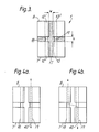
- Figures 5, 7a, 8a, 9a, 10 and 11 include schematic plan views of the switch of Figure 1 to indicate relevant driving current arrangements.
- a switch according to the present invention comprises a Fabry-Perot, semiconductor injection laser 1 mounted on a copper blade 2 between two pairs of current inputs 3, 4, 5, 6. Each end facet 7,8 of the laser 1 is exposed.
- the laser 1 is based on a GaAs substrate 11 with a number of layers of semiconductor material grown epitaxially onto it.
- Four contacts 12, 12 ⁇ and 13, 13 ⁇ comprise a double metal layer extending over the whole top surface of the laser 1 except for a transverse gap H, across the width of the laser 1, and a longitudinal gap W, which extends the length of the laser 1, between the two stripe windows 18, 19 in the dielectric layer 17.
- Each current input 3, 4, 5, 6 only is connected to a corresponding one of each of the contacts 12, 12 ⁇ , 13, 13 ⁇ which can then be driven independently of the other three contacts in each case.
- Each current input 3, 4, 5, 6 comprises a 1 mm wide copper conduction rail on a microstrip board 20, coupled to its respective contact by means of a gold wire and silver epoxy connection points (not shown).
- the structure and fabrication of the laser 1 are those conventional regarding a double heterostructure Ga (1-x) Al x As laser, x being 0.3.
- the substrate 11 is 100 ⁇ m thick, comprises Ga As and is metallised on its lowermost face 14. Onto the substrate 11 are grown, by conventional epitaxial growth techniques, four layers: a 2 ⁇ m layer 21 of n-doped Ga Al As; a 0.2 ⁇ m active layer 22 of Ga As; a 0.8 ⁇ m p-doped layer 15 of Ga Al As; and a 0.8 ⁇ m p-doped contact layer 16 of Ga As. Each of the doped layers is doped to a conventional level for use in semiconductor laser technology.
- the active layer 22 lies between two layers 21, 15 of higher band gap and lower refractive index material to give both optical and carrier confinement in a direction normal to the layers.
- the contact layer 16 Onto the contact layer 16 is deposited the dielectric layer 17 of SiO2. Two stripe windows 18, 19 are etched through the SiO2 down to the level of the contact layer 16. Zn is diffused onto the contact layer 16 in the region of the stripe windows 18, 19 to give doping levels of the order of 3 ⁇ 1017 cm ⁇ 3.
- a double metal layer of 3 ⁇ m of Au on 60 Angstroms of Ti is deposited on the dielectric layer 17 and into the stripe windows 18, 19, then etched to form the four contacts 12, 12 ⁇ , 13, 13 ⁇ by forming the transverse and longitudinal gaps H and W. Although both the Ti and the Au layers are etched to form the transverse gap H, only the Au layer is etched to form the longitudinal gap W.
- the laser 1 is 400 ⁇ m long, between its end facets 7, 8, and 200 ⁇ m wide, while each stripe window 18, 19 is 4 ⁇ m wide. The distance between the mid-heaven of the stripe windows 18, 19 is 7 ⁇ m.
- the transverse gap H is 15 ⁇ m wide. The resistance measured between each pair of contacts in a direction across the width of the laser 1 is about 60 ohms while that measured in a direction along the laser 1, traversing the transverse gap H, is about 900 ohms.
- each current input 3, 4, 5, 6 being connected via a 50 ohm chip resistor 23, 24 (only two shown) to an OSSM connector 25.
- Bias currents can be fed independently to each of the contacts 12, 12 ⁇ , 13, 13 ⁇ and trigger pulses can be superimposed on the bias current of any one or more of the contacts.
- the laser 1 can be used either to generate optical radiation by lasing or to amplify an optical input signal.
- the semiconductor injection laser 1 can be considered as providing two optical channels, each channel lying below one of the stripe windows 18, 19. It can lase or amplify in two or more different stable modes, light being carried in different distributions between the optical channels.
- light generated by the laser 1 may be confined to one optical channel or distributed between both.
- light input 40 to one of the channels may be carried and emitted from that channel, the switch being in a bar state as shown in figure 4a, or it may be coupled into and emitted from the other channel, the switch being in a cross state as shown in Figure 4b, or it may propagate in the channels in a combination of cross and bar states.
- the current to each contact 12, 12 ⁇ , 13, 13 ⁇ was designated i1, i2, i3, and i4 respectively.
- Variable currents i1 and i4 were fed to the other diagonal pair of contacts 12, 13 ⁇ , these currents being maintained equal to each other.
- the total light output from one end facet of the laser 1 was measured in mV using a photodetector.
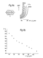
- the variable currents i1 and i4 were increased from zero, the light output remained substantially constant, increasing only a little, before showing a discontinuity and sharp increase 60 when the sum of i1 and i4 equalled slightly more than 100mA.
- the two values A, B lay either side of the sharp increase 60 in light output seen in Figure 5.
- the positions 26, 27 of the stripe windows, 18, 19 and therefore of the two optical channels, in relation to the light output distribution 28 were also recorded.
- the discontinuity in light output corresponded to a change in mode of the laser 1.
- the laser 1 emitted spontaneous light substantially from under the 26 of only one stripe window 18.
- the laser 1 was lasing, emitting light form under the positions 26, 27 of both stripe windows 18, 19.
- the laser 1 had switched from a first mode, in which light was generated in and emitted from only one optical channel, to a second mode, in which light was generated and emitted from both optical channels.
- the on/off ratio between the two bistable states was as large as 8:1.
- optical switching could be used in the above configuration, by replacing the electrical pulses with optical pulses, input to the ends of the waveguiding paths under the contacts.
- optical radiation of a wavelength corresponding to that of radiation generated by the laser 1 focussed onto different input positions of the laser facet, switching behaviour as described above with respect to 10ns electrical pulses can be achieved.
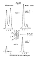
- near field measurements were carried out to plot the optical output across each facet 7, 8 of the laser 1 when driven to operate in different (lasing) modes.
- Figure 11a where similar drive currents were supplied to each of the four contacts, predominantly twin-peaked near fields were observed at each facet 7,8.
- a small interstripe peak 70 was also observed at one facet, resulting from interference between the curved wavefronts of the optical radiation emerging at the facet concerned.
- each optical output plot is plotted in the same transverse direction with respect to the laser 1).
- the total driving current supplied to the contacts in order to achieve the modes shown in Figure 11 was compared as a measure of the effective absorption in the laser 1 in each case.
- the threshold current for the bar state of Figure 11d was 175mA while those for the cross-coupled mode of Figure 11b and for the divided mode of Figure 11c were 399mA and 360mA respectively. This indicated increases in the effective absorption of 28% (22cm ⁇ 1) and 6% (4.5cm ⁇ 1) respectively.
- the drive currents i1, i2, i3, i4 may remain constant, at a level below any lasing threshold of the laser, and an optical input signal used to operate the switch.
- an optical input signal may be injected into a first optical channel of the laser 1 at an end facet 7.
- the signal should be of a wavelength suitable for amplification by the laser 1.
- the optical input signal may then be selectively switched to emerge from either of the optical channels at the other end of facet 8 of the laser 1.
- the contacts could again be driven at a current below any lasing threshold of the laser 1, and an optical input signal injected into a channel of the laser 1, but the optical trigger pulse could be replaced by an electrical trigger pulse to one or more of the contacts, superimposed on the driving current concerned.
- the present invention is directed to switching optical signals between alternative optical channels in a laser and should not be considered to be limited to switching between only two channels. For instance, there may be present a matrix of at least three optical channels between which an optical signal may be switched.
- two optical channels may share a common section.
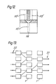
- a forked stripe window 118 may be provided which has three associated contacts 112, 112 ⁇ , 113 ⁇ .
- Two optical channels are then available which both incorporate one of the contacts 112, but which then diverge to follow each of the remaining contacts 112 ⁇ 113 ⁇ respectively.
- Such a switch could be controlled by means of electrical trigger pulses supplied to the remaining contacts 112 ⁇ , 113 ⁇ .
- the laser 1 of the embodiment described generates optical radiation of wavelength 0.8 ⁇ m but lasers which will generate or amplify different wavelengths may be substituted. Further, lasers of different structures, for instance having different contact arrangements, semiconductor materials or layer arrangements may be substituted.
- the transverse gap H should extend only through the Au/Ti contact material. It may also extend into the layers of semiconductor material. For instance opposing facets may be etched or ion milled into the semiconductor material. Under these circumstances, dielectric material could be used to fill the transverse gap H.
- the transverse gap H need not be uniformly parallel sided but may provide different distances between the pairs of contacts it separates along the laser 1. That is, between the segments of each optical channel. However the width of the transverse gap H between each of these pairs of contacts is preferably limited.
- the unpumped region of the switch produced by the gap H introduces absorption in the laser cavity. If the absorption is too high, absorptive bistability can occur, particularly where higher feedback is used, which reduces the speed of operation of the switch. To avoid the onset of significant absorptive effects in a Fabry Perot laser structure having facets of reflectivity of the order of 20%, it has been calculated that in a laser structure 400 microns long, the gap H should preferably be less than or equal to 40 microns.
- the onset of absorptive effects was found to depend on the ratio of currents, for instance, i2:i1, supplied to the contacts either side of the gap H in one of the stripe windows 18, 19.
- the ratio had to be kept small, for instance, of the order of 1:1.
- the ratio i2:i1 could be increased.
- a second constraint on the width of gap H is that it should be more than or equal to the distance between the mid-heaven of the stripe windows 18, 19 in the region of the gap H. This constraint is dictated by the requirement that optical coupling between the two different optical channels by diffraction is facilitated.
- width of the gap H and the length of the laser structure can be generalised as ratios generally applicable to laser structures of other lengths.
- an optical trigger pulse it need only be of a wavelength having sufficient photon energy to generate charge carriers in or near the optical channel to which it is input. These charge carriers then effect switching by changing the feedback characteristics, the optical gain, or the refractive index.
- the characteristics determining the optical channels may be varied. For instance refractive index guiding may be provided in a direction perpendicular to the direction of current flow. Further, the channels need not be straight. However the distance between the optical channels in the region of a discontinuity in the associated contacts, that is the distance between the longitudinal axes of the channels, should not be so great as to prevent diffractive coupling of radiation from one channel to the other. The latter distance is typically required to lie in the range form 2 ⁇ m to 10 ⁇ m inclusive but might be found satisfactory above that range where tight control over refractive index variations in the semiconductor materials is available.
- the switch of the present invention may act not just as an isolated switch but as part of a variable beam splitter or matrix switch.
- an array of lasers 1 might be joined to act in a matrix with light output 51 from the matrix being controlled by the pattern of light input 52 as well as by the associated pattern of drive currents to the electrical contacts (not shown).
- an example of such an extended device may have nine contacts 73, some of which may optionally be coupled together and some of which may optionally not require a driving current at all, depending on the application to which such a device is to be put.
- two extra contacts 90, 91 are provided after provision of a facet trench 92 in the optical channels provided by the stripe windows 18, 19.
- a facet trench 92 can be produced by wet chemical etching for instance.
- M Wade et al describe facet etching techniques.
- the facet trench 92 extends through the contact material into the layer above the active layer of the device and can be produced using known etchants for the relevant material of the layers.
- Devices according to embodiments of the present invention can be used to switch input optical signals, even when driven over the lasing threshold, since the signals appear, amplified, superimposed on the light generated by the laser structure.
Landscapes
- Physics & Mathematics (AREA)
- Nonlinear Science (AREA)
- General Physics & Mathematics (AREA)
- Optics & Photonics (AREA)
- Semiconductor Lasers (AREA)
- Switches With Compound Operations (AREA)
- Switches Operated By Changes In Physical Conditions (AREA)
- Keying Circuit Devices (AREA)
- Electronic Switches (AREA)
- Optical Integrated Circuits (AREA)
Priority Applications (1)
| Application Number | Priority Date | Filing Date | Title |
|---|---|---|---|
| AT87302059T ATE88300T1 (de) | 1986-03-10 | 1987-03-10 | Opto-elektronischer wechselschalter. |
Applications Claiming Priority (2)
| Application Number | Priority Date | Filing Date | Title |
|---|---|---|---|
| GB868605862A GB8605862D0 (en) | 1986-03-10 | 1986-03-10 | Opto-electronic directional switch |
| GB8605862 | 1986-03-10 |
Publications (3)
| Publication Number | Publication Date |
|---|---|
| EP0241143A2 true EP0241143A2 (de) | 1987-10-14 |
| EP0241143A3 EP0241143A3 (en) | 1988-02-03 |
| EP0241143B1 EP0241143B1 (de) | 1993-04-14 |
Family
ID=10594326
Family Applications (1)
| Application Number | Title | Priority Date | Filing Date |
|---|---|---|---|
| EP87302059A Expired - Lifetime EP0241143B1 (de) | 1986-03-10 | 1987-03-10 | Opto-elektronischer Wechselschalter |
Country Status (7)
| Country | Link |
|---|---|
| US (1) | US4809290A (de) |
| EP (1) | EP0241143B1 (de) |
| JP (1) | JPS6326637A (de) |
| AT (1) | ATE88300T1 (de) |
| CA (1) | CA1284836C (de) |
| DE (1) | DE3785382T2 (de) |
| GB (1) | GB8605862D0 (de) |
Cited By (2)
| Publication number | Priority date | Publication date | Assignee | Title |
|---|---|---|---|---|
| WO1991003760A1 (en) * | 1989-09-09 | 1991-03-21 | British Telecommunications Public Limited Company | Optically coupled waveguides |
| US5454058A (en) * | 1990-03-30 | 1995-09-26 | Bt&D Technologies, Ltd. | Selective optical signal switch and/or combiner |
Families Citing this family (7)
| Publication number | Priority date | Publication date | Assignee | Title |
|---|---|---|---|---|
| GB8805620D0 (en) * | 1988-03-09 | 1988-04-07 | British Telecomm | Polarisation switching in active devices |
| JP2656598B2 (ja) * | 1989-01-30 | 1997-09-24 | 株式会社日立製作所 | 半導体光スイッチ及び半導体光スイッチアレイ |
| JPH0693532B2 (ja) * | 1990-03-27 | 1994-11-16 | 工業技術院長 | 半導体レーザ |
| US5052006A (en) * | 1990-12-18 | 1991-09-24 | Thermo Electron Technologies Corp. | Scanner beam semiconductor switching apparatus |
| JP3154241B2 (ja) * | 1991-11-22 | 2001-04-09 | 古河電気工業株式会社 | 半導体光部品とその製造方法 |
| US6272163B1 (en) * | 1999-02-24 | 2001-08-07 | Agere Systems Inc. | Method for fabricating high speed Fabry-Perot lasers for data communication |
| US6775312B2 (en) * | 2002-05-15 | 2004-08-10 | Quantum Devices, Inc. | Photonic integrated circuit |
Family Cites Families (5)
| Publication number | Priority date | Publication date | Assignee | Title |
|---|---|---|---|---|
| US3436679A (en) * | 1966-03-07 | 1969-04-01 | Gen Electric | Semiconductor junction laser with electronically displaceable and deflectable beam |
| US3465159A (en) * | 1966-06-27 | 1969-09-02 | Us Army | Light amplifying device |
| US4219785A (en) * | 1978-06-26 | 1980-08-26 | Xerox Corporation | Optical beam scanning by phase delays |
| US4210803A (en) * | 1979-03-15 | 1980-07-01 | University Of Delaware | Method and apparatus for signal transmission via an optical fiber |
| JPS60149030A (ja) * | 1983-12-21 | 1985-08-06 | Nec Corp | 光スイツチ |
-
1986
- 1986-03-10 GB GB868605862A patent/GB8605862D0/en active Pending
-
1987
- 1987-03-09 CA CA000531528A patent/CA1284836C/en not_active Expired - Lifetime
- 1987-03-10 JP JP62056420A patent/JPS6326637A/ja active Pending
- 1987-03-10 DE DE87302059T patent/DE3785382T2/de not_active Expired - Fee Related
- 1987-03-10 US US07/024,129 patent/US4809290A/en not_active Expired - Fee Related
- 1987-03-10 EP EP87302059A patent/EP0241143B1/de not_active Expired - Lifetime
- 1987-03-10 AT AT87302059T patent/ATE88300T1/de not_active IP Right Cessation
Cited By (2)
| Publication number | Priority date | Publication date | Assignee | Title |
|---|---|---|---|---|
| WO1991003760A1 (en) * | 1989-09-09 | 1991-03-21 | British Telecommunications Public Limited Company | Optically coupled waveguides |
| US5454058A (en) * | 1990-03-30 | 1995-09-26 | Bt&D Technologies, Ltd. | Selective optical signal switch and/or combiner |
Also Published As
| Publication number | Publication date |
|---|---|
| GB8605862D0 (en) | 1986-04-16 |
| EP0241143B1 (de) | 1993-04-14 |
| US4809290A (en) | 1989-02-28 |
| DE3785382D1 (de) | 1993-05-19 |
| EP0241143A3 (en) | 1988-02-03 |
| CA1284836C (en) | 1991-06-11 |
| JPS6326637A (ja) | 1988-02-04 |
| DE3785382T2 (de) | 1993-11-18 |
| ATE88300T1 (de) | 1993-04-15 |
Similar Documents
| Publication | Publication Date | Title |
|---|---|---|
| EP0641049B1 (de) | Optischer Halbleitervorrichtung und Herstellungsverfahren | |
| US7112827B2 (en) | Tunable wavelength laser | |
| EP0851548B1 (de) | Optischer Halbleiterverstärker | |
| US6639241B2 (en) | Optical device using semiconductor | |
| EP0692853B1 (de) | Wellenlängenabstimmbarer Halbleiterlaser | |
| US6111998A (en) | Semiconductor optical device, fiber optical amplifier and optical transmission system | |
| EP0378098B1 (de) | Optische Halbleitervorrichtung | |
| EP0241143B1 (de) | Opto-elektronischer Wechselschalter | |
| JP3284994B2 (ja) | 半導体光集積素子及びその製造方法 | |
| US5742423A (en) | Semiconductor optical modulator | |
| US4947400A (en) | Laser-photodetector assemblage | |
| US5239600A (en) | Optical device with an optical coupler for effecting light branching/combining by splitting a wavefront of light | |
| EP0332446B1 (de) | Polarisationsumschaltung in aktiven Elementen | |
| JPH04783A (ja) | 半導体光素子 | |
| US20010026671A1 (en) | Waveguide optical device | |
| EP1263099B1 (de) | Halbleiterlaser | |
| US5675602A (en) | Optical integrated circuit device and driving method therefor | |
| JP2004311556A (ja) | 半導体レーザ並びにそれを用いた光モジュール及び機能集積型レーザ | |
| EP0269061A2 (de) | Optische Filtervorrichtung | |
| JPS6136987A (ja) | 光検出器付分布帰還形半導体レ−ザ | |
| JP3154417B2 (ja) | 半導体レーザの発振波長制御駆動方法 | |
| CN112350148A (zh) | 半导体光学元件和包括该元件的半导体光学装置 | |
| JP3255111B2 (ja) | 半導体レーザ及びその製造方法 | |
| EP1309050A1 (de) | Laservorrichtung und Verfahren | |
| JPH07312457A (ja) | 半導体レーザ装置 |
Legal Events
| Date | Code | Title | Description |
|---|---|---|---|
| PUAI | Public reference made under article 153(3) epc to a published international application that has entered the european phase |
Free format text: ORIGINAL CODE: 0009012 |
|
| AK | Designated contracting states |
Kind code of ref document: A2 Designated state(s): AT BE CH DE ES FR GB GR IT LI LU NL SE |
|
| PUAL | Search report despatched |
Free format text: ORIGINAL CODE: 0009013 |
|
| AK | Designated contracting states |
Kind code of ref document: A3 Designated state(s): AT BE CH DE ES FR GB GR IT LI LU NL SE |
|
| 17P | Request for examination filed |
Effective date: 19880414 |
|
| 17Q | First examination report despatched |
Effective date: 19910327 |
|
| GRAA | (expected) grant |
Free format text: ORIGINAL CODE: 0009210 |
|
| AK | Designated contracting states |
Kind code of ref document: B1 Designated state(s): AT BE CH DE ES FR GB GR IT LI LU NL SE |
|
| PG25 | Lapsed in a contracting state [announced via postgrant information from national office to epo] |
Ref country code: LI Effective date: 19930414 Ref country code: GR Free format text: LAPSE BECAUSE OF FAILURE TO SUBMIT A TRANSLATION OF THE DESCRIPTION OR TO PAY THE FEE WITHIN THE PRESCRIBED TIME-LIMIT Effective date: 19930414 Ref country code: CH Effective date: 19930414 Ref country code: BE Effective date: 19930414 Ref country code: AT Effective date: 19930414 |
|
| REF | Corresponds to: |
Ref document number: 88300 Country of ref document: AT Date of ref document: 19930415 Kind code of ref document: T |
|
| REF | Corresponds to: |
Ref document number: 3785382 Country of ref document: DE Date of ref document: 19930519 |
|
| ITF | It: translation for a ep patent filed | ||
| PG25 | Lapsed in a contracting state [announced via postgrant information from national office to epo] |
Ref country code: ES Free format text: LAPSE BECAUSE OF FAILURE TO SUBMIT A TRANSLATION OF THE DESCRIPTION OR TO PAY THE FEE WITHIN THE PRESCRIBED TIME-LIMIT Effective date: 19930725 |
|
| REG | Reference to a national code |
Ref country code: CH Ref legal event code: PL |
|
| ET | Fr: translation filed | ||
| PLBE | No opposition filed within time limit |
Free format text: ORIGINAL CODE: 0009261 |
|
| STAA | Information on the status of an ep patent application or granted ep patent |
Free format text: STATUS: NO OPPOSITION FILED WITHIN TIME LIMIT |
|
| PG25 | Lapsed in a contracting state [announced via postgrant information from national office to epo] |
Ref country code: LU Free format text: LAPSE BECAUSE OF NON-PAYMENT OF DUE FEES Effective date: 19940331 |
|
| 26N | No opposition filed | ||
| EAL | Se: european patent in force in sweden |
Ref document number: 87302059.8 |
|
| PGFP | Annual fee paid to national office [announced via postgrant information from national office to epo] |
Ref country code: FR Payment date: 19950208 Year of fee payment: 9 |
|
| PGFP | Annual fee paid to national office [announced via postgrant information from national office to epo] |
Ref country code: SE Payment date: 19950213 Year of fee payment: 9 |
|
| PGFP | Annual fee paid to national office [announced via postgrant information from national office to epo] |
Ref country code: GB Payment date: 19950216 Year of fee payment: 9 |
|
| PGFP | Annual fee paid to national office [announced via postgrant information from national office to epo] |
Ref country code: DE Payment date: 19950217 Year of fee payment: 9 |
|
| PGFP | Annual fee paid to national office [announced via postgrant information from national office to epo] |
Ref country code: NL Payment date: 19950331 Year of fee payment: 9 |
|
| PG25 | Lapsed in a contracting state [announced via postgrant information from national office to epo] |
Ref country code: GB Effective date: 19960310 |
|
| PG25 | Lapsed in a contracting state [announced via postgrant information from national office to epo] |
Ref country code: SE Effective date: 19960311 |
|
| PG25 | Lapsed in a contracting state [announced via postgrant information from national office to epo] |
Ref country code: NL Effective date: 19961001 |
|
| GBPC | Gb: european patent ceased through non-payment of renewal fee |
Effective date: 19960310 |
|
| PG25 | Lapsed in a contracting state [announced via postgrant information from national office to epo] |
Ref country code: FR Effective date: 19961129 |
|
| NLV4 | Nl: lapsed or anulled due to non-payment of the annual fee |
Effective date: 19961001 |
|
| PG25 | Lapsed in a contracting state [announced via postgrant information from national office to epo] |
Ref country code: DE Effective date: 19961203 |
|
| EUG | Se: european patent has lapsed |
Ref document number: 87302059.8 |
|
| REG | Reference to a national code |
Ref country code: FR Ref legal event code: ST |
|
| PG25 | Lapsed in a contracting state [announced via postgrant information from national office to epo] |
Ref country code: IT Free format text: LAPSE BECAUSE OF NON-PAYMENT OF DUE FEES;WARNING: LAPSES OF ITALIAN PATENTS WITH EFFECTIVE DATE BEFORE 2007 MAY HAVE OCCURRED AT ANY TIME BEFORE 2007. THE CORRECT EFFECTIVE DATE MAY BE DIFFERENT FROM THE ONE RECORDED. Effective date: 20050310 |