EP0241873A2 - Fabrication de dispositifs à semi-conducteur en utilisant comme patrons des couches métalliques - Google Patents
Fabrication de dispositifs à semi-conducteur en utilisant comme patrons des couches métalliques Download PDFInfo
- Publication number
- EP0241873A2 EP0241873A2 EP87105317A EP87105317A EP0241873A2 EP 0241873 A2 EP0241873 A2 EP 0241873A2 EP 87105317 A EP87105317 A EP 87105317A EP 87105317 A EP87105317 A EP 87105317A EP 0241873 A2 EP0241873 A2 EP 0241873A2
- Authority
- EP
- European Patent Office
- Prior art keywords
- metal
- substrate
- growth
- molecules
- patterned metal
- Prior art date
- Legal status (The legal status is an assumption and is not a legal conclusion. Google has not performed a legal analysis and makes no representation as to the accuracy of the status listed.)
- Granted
Links
Images

Classifications
-
- H—ELECTRICITY
- H10—SEMICONDUCTOR DEVICES; ELECTRIC SOLID-STATE DEVICES NOT OTHERWISE PROVIDED FOR
- H10P—GENERIC PROCESSES OR APPARATUS FOR THE MANUFACTURE OR TREATMENT OF DEVICES COVERED BY CLASS H10
- H10P14/00—Formation of materials, e.g. in the shape of layers or pillars
- H10P14/40—Formation of materials, e.g. in the shape of layers or pillars of conductive or resistive materials
- H10P14/412—Deposition of metallic or metal-silicide materials
-
- C—CHEMISTRY; METALLURGY
- C23—COATING METALLIC MATERIAL; COATING MATERIAL WITH METALLIC MATERIAL; CHEMICAL SURFACE TREATMENT; DIFFUSION TREATMENT OF METALLIC MATERIAL; COATING BY VACUUM EVAPORATION, BY SPUTTERING, BY ION IMPLANTATION OR BY CHEMICAL VAPOUR DEPOSITION, IN GENERAL; INHIBITING CORROSION OF METALLIC MATERIAL OR INCRUSTATION IN GENERAL
- C23C—COATING METALLIC MATERIAL; COATING MATERIAL WITH METALLIC MATERIAL; SURFACE TREATMENT OF METALLIC MATERIAL BY DIFFUSION INTO THE SURFACE, BY CHEMICAL CONVERSION OR SUBSTITUTION; COATING BY VACUUM EVAPORATION, BY SPUTTERING, BY ION IMPLANTATION OR BY CHEMICAL VAPOUR DEPOSITION, IN GENERAL
- C23C16/00—Chemical coating by decomposition of gaseous compounds, without leaving reaction products of surface material in the coating, i.e. chemical vapour deposition [CVD] processes
- C23C16/44—Chemical coating by decomposition of gaseous compounds, without leaving reaction products of surface material in the coating, i.e. chemical vapour deposition [CVD] processes characterised by the method of coating
- C23C16/48—Chemical coating by decomposition of gaseous compounds, without leaving reaction products of surface material in the coating, i.e. chemical vapour deposition [CVD] processes characterised by the method of coating by irradiation, e.g. photolysis, radiolysis, particle radiation
- C23C16/483—Chemical coating by decomposition of gaseous compounds, without leaving reaction products of surface material in the coating, i.e. chemical vapour deposition [CVD] processes characterised by the method of coating by irradiation, e.g. photolysis, radiolysis, particle radiation using coherent light, UV to IR, e.g. lasers
-
- H—ELECTRICITY
- H10—SEMICONDUCTOR DEVICES; ELECTRIC SOLID-STATE DEVICES NOT OTHERWISE PROVIDED FOR
- H10D—INORGANIC ELECTRIC SEMICONDUCTOR DEVICES
- H10D64/00—Electrodes of devices having potential barriers
- H10D64/01—Manufacture or treatment
- H10D64/011—Manufacture or treatment of electrodes ohmically coupled to a semiconductor
- H10D64/0111—Manufacture or treatment of electrodes ohmically coupled to a semiconductor to Group IV semiconductors
-
- H—ELECTRICITY
- H10—SEMICONDUCTOR DEVICES; ELECTRIC SOLID-STATE DEVICES NOT OTHERWISE PROVIDED FOR
- H10D—INORGANIC ELECTRIC SEMICONDUCTOR DEVICES
- H10D64/00—Electrodes of devices having potential barriers
- H10D64/01—Manufacture or treatment
- H10D64/011—Manufacture or treatment of electrodes ohmically coupled to a semiconductor
- H10D64/0116—Manufacture or treatment of electrodes ohmically coupled to a semiconductor to Group III-V semiconductors
-
- Y—GENERAL TAGGING OF NEW TECHNOLOGICAL DEVELOPMENTS; GENERAL TAGGING OF CROSS-SECTIONAL TECHNOLOGIES SPANNING OVER SEVERAL SECTIONS OF THE IPC; TECHNICAL SUBJECTS COVERED BY FORMER USPC CROSS-REFERENCE ART COLLECTIONS [XRACs] AND DIGESTS
- Y10—TECHNICAL SUBJECTS COVERED BY FORMER USPC
- Y10S—TECHNICAL SUBJECTS COVERED BY FORMER USPC CROSS-REFERENCE ART COLLECTIONS [XRACs] AND DIGESTS
- Y10S438/00—Semiconductor device manufacturing: process
- Y10S438/903—Catalyst aided deposition
Definitions
- This invention relates generally to a method of fabricating semiconductor devices which includes growing patterned metal layers and particularly to such a method which uses laser activated chemical vapor deposition.
- a patterned metal layer may be grown directly on a substrate by illuminating the substrate, which is heated to an elevated temperature, with the desired pattern in the presence of a metal-containing gas which is adsorbed at subatmospheric pressure thereby decomposing the adsorbed metal-containing molecules. The radiation is then turned off, and the metal present on the surface catalyzes the growth of additional metal.
- the patterned metal comprises aluminum and the metal-containing gas comprises triisobutylaluminum. Depending upon the intensity of the initial illumination, either a positive or negative image of the pattern may be produced.
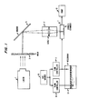
- FIG. 1 A schematic representation of apparatus useful for practicing a method of this invention is depicted in FIG. 1. Depicted are light source 1, mask 3, mirror 5, growth chamber 7, mass flow controllers 9 and 11, gas reservoir 13, and pump 15. Lens 17 permits the mask image to be imaged onto the substrate.
- the reservoir contains the metal-containing molecule.
- Gas source 19 is used if a carrier gas is desired.
- the light source was a excimer laser, such as one using KrF, which operated at a repetition rate of 100 Hz. Such lasers are desirable because of, for example, their relatively high intensity output. The precise repetition rate is not critical. It should, of course, emit at a frequency absorbed by the molecule.
- the power delivered to the substrate determines whether a positive or negative image is produced. A low power level produces growth in the illuminated areas, by photolyzing said adsorbed molecules, while a high power level produces growth in the non-illuminated areas. High power is believed to result in gas phase reactions with the products diffusing to the non-illuminated areas while inhibiting growth in the illuminated areas for reasons not perfectly understood.
- the growth chamber was a stainless steel cell which desirably has heating means which enable the substrate temperature to be raised during growth. It has been found desirable to heat only the substrate at approximately 250°C with the remainder of the chamber remaining only slightly above ambient temperature.
- the reactant molecules are transported to the growth chamber through stainless steel tubing from the reservoir. It has been found desirable to grow at growth chamber pressures between 6.7 Pa and 20 Pa (.05 and .15 Tprr). Lesser pressures lead to undesirably slow growth rates, and higher pressures lead to bad growth morphology.
- the molecule should surface react to leave metal behind when irradiated.
- the radiation will typically be light from, e.g., a laser, capable of decomposing the molecule although it is to be understood that electron or ion beams might also be used to achieve the same decomposition.
- a carrier gas is generally not used except for flushing the growth chamber.
- a carrier gas e.g., H 2 , is required for the surface catalysis reaction.
- the desired substrate is solvent degreased, acid etched, rinsed in de-ionized water, and blown dry with, for example, N 2 . These preparatory steps are well known in the semiconductor art and need not be described in more detail. It is then placed in the growth chamber, and the substrate temperature is raised to approximately 250 o C. After the cell temperature has stabilized, the reactant gas and H 2 are allowed to flow through the cell to purge it of contaminants. After purging has been completed, the flow of H 2 is stopped, and the substrate is illuminated through the illumination system depicted. A typical duration of the illumination period is between 15 and 600 seconds with each pulse depositing approximately 10-20 mJ/cm 2 at the substrate surface.
- the reactant molecule is triisobutylaluminum (TIBA).
- Tsao used a highly localized heat source, namely, a C0 2 laser focused to approximately 100 pm for the thermal growth segment of their process. It is believed that TIBA decomposes into diisobutylaluminum-hydride (DIBAH) as well as butylenes at temperatures above 50°C.
- DIBAH diisobutylaluminum-hydride
- DIBAH has an equilibrium vapor pressure which is lower than that of TIBA and adlayers can form at lower pressure or at significantly higher temperatures. If it is additionally assumed that these layers have a substantial residence time on the substrate, the hypothesis that laser activation involves a surface photoreaction becomes plausible. T sao was probably unable to create a significant DIBAH partial pressure because he heated only a small area of material and thus did not form the requisite adlayer.
- Selectivity obtained when Al was deposited on preexisting Al wires means that the native oxide on the A1 is sufficient to block non-selective growth, since Al would certainly grow on Al.
- extremely good, i.e., low resistance, Al/ A l contacts were obtained.
- the native oxide in conventional deposition technique blocks contact formation. This result for multilevel interconnects is important.
- the surface need not be chemically uniform. For example, good results were also obtained when openings were selectively made in an Si0 2 layer on Si. This is obviously important for making field effect transistors. Also, good conformal coverage was obtained, as growth was obtained on both the oxide and the oxide cuts.
- the degree of spatial selectivity on the surface of a GaAs substrate is also surprising because this surface is not chemically inert. For example, it is known that it acts to catalytically decompose trimethylgallium and arsine to grow GaAs. It is believed that several monolayers of native oxide are formed prior to introducing the substrate into the growth chamber and these are sufficient to block the surface reaction.
- oxide layers may be detrimental to the usefulness of this method for making devices if present in undesired quantity.
- Depositions were performed on lightly doped n-type GaAs as an initial test of the quality of contacts formed.
- a representative I-V characteristic curve is depicted in FIG. 2. This figure depicts the current vertically in units of 20pa per division and voltage horizontally in units of 5 volts per division. The particular device is a dot approximately 25pm in diameter and the curve indicates that diode like behavior is obtained.
- the reverse breakdown voltage between 15-18 volts, is typical of GaAs and indicates that no substantial substrate damage occurred during the laser activation process.
- the relatively high forward biased turn-on voltage approximately 1-2 volts, suggests the presence of a small amount of surface oxide.
- the resistivity of the metal features produced approaches that of bulk Al indicating that high speed operation can be obtained.
- Al atoms can be used to dope Si p-type thereby, for example, forming a p-n junction if the Si were initially n-type or forming ohmic contacts if the Si is p-type or n + .
- Ohmic contacts have been fabricated and are good candidates for source and drain contacts for field effect transistors (FET) since metal depositions on Si0 2 are used for FET gates. Complete transistor fabrication is envisioned and has been demonstrated. It is desirable to anneal, after deposition, at a temperature between 450 and 600°C for a time between 1 and 10 minutes.
- the reactant gas need not be a metal-organic molecule. Any system which grows by surface catalysis can be used.
Landscapes
- Chemical & Material Sciences (AREA)
- Chemical Kinetics & Catalysis (AREA)
- Materials Engineering (AREA)
- Toxicology (AREA)
- Optics & Photonics (AREA)
- General Chemical & Material Sciences (AREA)
- Physics & Mathematics (AREA)
- Engineering & Computer Science (AREA)
- Health & Medical Sciences (AREA)
- Mechanical Engineering (AREA)
- Metallurgy (AREA)
- Organic Chemistry (AREA)
- Chemical Vapour Deposition (AREA)
- Chemically Coating (AREA)
- Electrodes Of Semiconductors (AREA)
Applications Claiming Priority (2)
| Application Number | Priority Date | Filing Date | Title |
|---|---|---|---|
| US06/853,676 US4701347A (en) | 1986-04-18 | 1986-04-18 | Method for growing patterned metal layers |
| US853676 | 1992-03-19 |
Publications (3)
| Publication Number | Publication Date |
|---|---|
| EP0241873A2 true EP0241873A2 (fr) | 1987-10-21 |
| EP0241873A3 EP0241873A3 (en) | 1989-12-27 |
| EP0241873B1 EP0241873B1 (fr) | 1993-10-06 |
Family
ID=25316628
Family Applications (1)
| Application Number | Title | Priority Date | Filing Date |
|---|---|---|---|
| EP87105317A Expired - Lifetime EP0241873B1 (fr) | 1986-04-18 | 1987-04-10 | Fabrication de dispositifs à semi-conducteur en utilisant comme patrons des couches métalliques |
Country Status (5)
| Country | Link |
|---|---|
| US (1) | US4701347A (fr) |
| EP (1) | EP0241873B1 (fr) |
| JP (1) | JPS62296421A (fr) |
| CA (1) | CA1270070A (fr) |
| DE (1) | DE3787662T2 (fr) |
Cited By (2)
| Publication number | Priority date | Publication date | Assignee | Title |
|---|---|---|---|---|
| DE3730644A1 (de) * | 1987-09-11 | 1989-03-30 | Baeuerle Dieter | Verfahren zur vorgegeben strukturierten abscheidung von mikrostrukturen mit laserlicht |
| EP0470784A3 (en) * | 1990-08-10 | 1993-03-03 | Motorola Inc. | Method for selectively depositing a thin film |
Families Citing this family (12)
| Publication number | Priority date | Publication date | Assignee | Title |
|---|---|---|---|---|
| US5264108A (en) * | 1992-09-08 | 1993-11-23 | The United States Of America As Represented By The United States Department Of Energy | Laser patterning of laminated structures for electroplating |
| JPH0737887A (ja) * | 1993-07-22 | 1995-02-07 | Mitsubishi Electric Corp | 配線形成方法,配線修復方法,及び配線パターン変更方法 |
| US6878417B2 (en) | 1997-11-12 | 2005-04-12 | John C. Polanyi | Method of molecular-scale pattern imprinting at surfaces |
| US6319566B1 (en) | 1997-11-12 | 2001-11-20 | John C. Polanyi | Method of molecular-scale pattern imprinting at surfaces |
| US6156393A (en) * | 1997-11-12 | 2000-12-05 | John C. Polanyi | Method of molecular-scale pattern imprinting at surfaces |
| US6248658B1 (en) | 1999-01-13 | 2001-06-19 | Advanced Micro Devices, Inc. | Method of forming submicron-dimensioned metal patterns |
| JP2004356134A (ja) * | 2003-05-27 | 2004-12-16 | Canon Inc | 微小構造の加工方法、該加工法を用いて作製した微小素子の作製方法、微小素子 |
| KR20070112870A (ko) * | 2005-03-22 | 2007-11-27 | 셀 인터나쵸나아레 레사아치 마아츠샤피 비이부이 | 반응기 시스템 및 에틸렌옥사이드의 제조방법 |
| US20090208672A1 (en) * | 2008-01-30 | 2009-08-20 | Polanyi John C | Method of linear patterning at surfaces |
| US10727317B2 (en) | 2018-10-04 | 2020-07-28 | International Business Machines Corporation | Bottom contact formation for vertical transistor devices |
| WO2020207759A1 (fr) * | 2019-04-12 | 2020-10-15 | Asml Netherlands B.V. | Procédé et appareil de formation de couche de matériau à motif |
| US20230279544A1 (en) * | 2020-09-03 | 2023-09-07 | Tcm Research Ltd. | Additive chemical vapor deposition methods and systems |
Family Cites Families (6)
| Publication number | Priority date | Publication date | Assignee | Title |
|---|---|---|---|---|
| US3061465A (en) * | 1959-10-09 | 1962-10-30 | Ethyl Corp | Method of metal plating with a group iv-b organometallic compound |
| US3271180A (en) * | 1962-06-19 | 1966-09-06 | Ibm | Photolytic processes for fabricating thin film patterns |
| US4133908A (en) * | 1977-11-03 | 1979-01-09 | Western Electric Company, Inc. | Method for depositing a metal on a surface |
| US4340617A (en) * | 1980-05-19 | 1982-07-20 | Massachusetts Institute Of Technology | Method and apparatus for depositing a material on a surface |
| WO1983004269A1 (fr) * | 1982-06-01 | 1983-12-08 | Massachusetts Institute Of Technology | Formation de films a motifs sans l'utilisation de masque |
| US4451503A (en) * | 1982-06-30 | 1984-05-29 | International Business Machines Corporation | Photo deposition of metals with far UV radiation |
-
1986
- 1986-04-18 US US06/853,676 patent/US4701347A/en not_active Expired - Fee Related
-
1987
- 1987-04-10 EP EP87105317A patent/EP0241873B1/fr not_active Expired - Lifetime
- 1987-04-10 DE DE87105317T patent/DE3787662T2/de not_active Expired - Fee Related
- 1987-04-16 CA CA000534963A patent/CA1270070A/fr not_active Expired
- 1987-04-18 JP JP62094332A patent/JPS62296421A/ja active Pending
Cited By (2)
| Publication number | Priority date | Publication date | Assignee | Title |
|---|---|---|---|---|
| DE3730644A1 (de) * | 1987-09-11 | 1989-03-30 | Baeuerle Dieter | Verfahren zur vorgegeben strukturierten abscheidung von mikrostrukturen mit laserlicht |
| EP0470784A3 (en) * | 1990-08-10 | 1993-03-03 | Motorola Inc. | Method for selectively depositing a thin film |
Also Published As
| Publication number | Publication date |
|---|---|
| DE3787662D1 (de) | 1993-11-11 |
| EP0241873B1 (fr) | 1993-10-06 |
| US4701347A (en) | 1987-10-20 |
| EP0241873A3 (en) | 1989-12-27 |
| JPS62296421A (ja) | 1987-12-23 |
| CA1270070A (fr) | 1990-06-05 |
| DE3787662T2 (de) | 1994-02-03 |
Similar Documents
| Publication | Publication Date | Title |
|---|---|---|
| US4701347A (en) | Method for growing patterned metal layers | |
| US4451503A (en) | Photo deposition of metals with far UV radiation | |
| US4608117A (en) | Maskless growth of patterned films | |
| KR100267145B1 (ko) | 박막트랜지스터 제작방법 | |
| GB2097820A (en) | Radiation induced deposition of metal on semiconductor surfaces | |
| CN105103271B (zh) | 用于脉冲式光激发沉积与蚀刻的装置与方法 | |
| US6348367B1 (en) | Method for manufacturing a semiconductor device | |
| JPH1050624A (ja) | 化学元素の受容材料中への導入方法 | |
| WO1990001794A1 (fr) | Procede de formation d'un mince film semi-conducteur et appareil de realisation dudit procede | |
| US5817559A (en) | Production method for a semiconductor device | |
| JPH11135436A (ja) | 化合物半導体膜の形成方法 | |
| JP3157911B2 (ja) | 化合物半導体基板の熱処理方法及びその熱処理装置 | |
| Micheli et al. | Laser microfabrication of thin films: Part one | |
| JPH0337186A (ja) | 化合物半導体薄膜の形成方法 | |
| Esrom et al. | Uv Excimer Laser Induced Prenucleation of Surfaces from Spin-on Films Followed by Electroless Metallization | |
| EP0248883B1 (fr) | Procede de depot selectif | |
| JPH08264460A (ja) | 窒素化合物半導体結晶成長方法および成長装置 | |
| Osgood Jr | An Overview of Laser Chemical Processing | |
| JP2832982B2 (ja) | 薄膜形成方法 | |
| KR20000015506A (ko) | 광 조사에 의한 원자층 증착 방법을 이용한 선택적 박막 형성방법 및 장치 | |
| JPS60167316A (ja) | 被膜の形成方法 | |
| JPH01215019A (ja) | オーミック電極の形成方法 | |
| JPH05251369A (ja) | 有機金属化学気相成長方法 | |
| JPH0443631A (ja) | 化合物半導体結晶の成長方法およびその実施のための装置 | |
| KR20020021871A (ko) | 레이저를 이용하는 질화물반도체의 억셉터 활성화 방법 |
Legal Events
| Date | Code | Title | Description |
|---|---|---|---|
| PUAI | Public reference made under article 153(3) epc to a published international application that has entered the european phase |
Free format text: ORIGINAL CODE: 0009012 |
|
| AK | Designated contracting states |
Kind code of ref document: A2 Designated state(s): DE FR GB IT NL |
|
| RTI1 | Title (correction) | ||
| PUAL | Search report despatched |
Free format text: ORIGINAL CODE: 0009013 |
|
| AK | Designated contracting states |
Kind code of ref document: A3 Designated state(s): DE FR GB IT NL |
|
| 17P | Request for examination filed |
Effective date: 19900514 |
|
| 17Q | First examination report despatched |
Effective date: 19910627 |
|
| GRAA | (expected) grant |
Free format text: ORIGINAL CODE: 0009210 |
|
| AK | Designated contracting states |
Kind code of ref document: B1 Designated state(s): DE FR GB IT NL |
|
| REF | Corresponds to: |
Ref document number: 3787662 Country of ref document: DE Date of ref document: 19931111 |
|
| ET | Fr: translation filed | ||
| ITF | It: translation for a ep patent filed | ||
| PGFP | Annual fee paid to national office [announced via postgrant information from national office to epo] |
Ref country code: GB Payment date: 19940325 Year of fee payment: 8 |
|
| PGFP | Annual fee paid to national office [announced via postgrant information from national office to epo] |
Ref country code: DE Payment date: 19940405 Year of fee payment: 8 |
|
| PGFP | Annual fee paid to national office [announced via postgrant information from national office to epo] |
Ref country code: FR Payment date: 19940408 Year of fee payment: 8 |
|
| PGFP | Annual fee paid to national office [announced via postgrant information from national office to epo] |
Ref country code: NL Payment date: 19940430 Year of fee payment: 8 |
|
| RAP4 | Party data changed (patent owner data changed or rights of a patent transferred) |
Owner name: AT&T CORP. |
|
| PLBE | No opposition filed within time limit |
Free format text: ORIGINAL CODE: 0009261 |
|
| STAA | Information on the status of an ep patent application or granted ep patent |
Free format text: STATUS: NO OPPOSITION FILED WITHIN TIME LIMIT |
|
| 26N | No opposition filed | ||
| PG25 | Lapsed in a contracting state [announced via postgrant information from national office to epo] |
Ref country code: GB Effective date: 19950410 |
|
| PG25 | Lapsed in a contracting state [announced via postgrant information from national office to epo] |
Ref country code: NL Effective date: 19951101 |
|
| GBPC | Gb: european patent ceased through non-payment of renewal fee |
Effective date: 19950410 |
|
| PG25 | Lapsed in a contracting state [announced via postgrant information from national office to epo] |
Ref country code: FR Effective date: 19951229 |
|
| NLV4 | Nl: lapsed or anulled due to non-payment of the annual fee |
Effective date: 19951101 |
|
| PG25 | Lapsed in a contracting state [announced via postgrant information from national office to epo] |
Ref country code: DE Effective date: 19960103 |
|
| REG | Reference to a national code |
Ref country code: FR Ref legal event code: ST |
|
| PG25 | Lapsed in a contracting state [announced via postgrant information from national office to epo] |
Ref country code: IT Free format text: LAPSE BECAUSE OF NON-PAYMENT OF DUE FEES;WARNING: LAPSES OF ITALIAN PATENTS WITH EFFECTIVE DATE BEFORE 2007 MAY HAVE OCCURRED AT ANY TIME BEFORE 2007. THE CORRECT EFFECTIVE DATE MAY BE DIFFERENT FROM THE ONE RECORDED. Effective date: 20050410 |