EP0243621B1 - Lötverfahren und Gerät - Google Patents
Lötverfahren und Gerät Download PDFInfo
- Publication number
- EP0243621B1 EP0243621B1 EP87103203A EP87103203A EP0243621B1 EP 0243621 B1 EP0243621 B1 EP 0243621B1 EP 87103203 A EP87103203 A EP 87103203A EP 87103203 A EP87103203 A EP 87103203A EP 0243621 B1 EP0243621 B1 EP 0243621B1
- Authority
- EP
- European Patent Office
- Prior art keywords
- fluid
- substrate
- temperature
- solder
- contact
- Prior art date
- Legal status (The legal status is an assumption and is not a legal conclusion. Google has not performed a legal analysis and makes no representation as to the accuracy of the status listed.)
- Expired - Lifetime
Links
Images


Classifications
-
- B—PERFORMING OPERATIONS; TRANSPORTING
- B23—MACHINE TOOLS; METAL-WORKING NOT OTHERWISE PROVIDED FOR
- B23K—SOLDERING OR UNSOLDERING; WELDING; CLADDING OR PLATING BY SOLDERING OR WELDING; CUTTING BY APPLYING HEAT LOCALLY, e.g. FLAME CUTTING; WORKING BY LASER BEAM
- B23K1/00—Soldering, e.g. brazing, or unsoldering
- B23K1/012—Soldering with the use of hot gas
-
- B—PERFORMING OPERATIONS; TRANSPORTING
- B23—MACHINE TOOLS; METAL-WORKING NOT OTHERWISE PROVIDED FOR
- B23K—SOLDERING OR UNSOLDERING; WELDING; CLADDING OR PLATING BY SOLDERING OR WELDING; CUTTING BY APPLYING HEAT LOCALLY, e.g. FLAME CUTTING; WORKING BY LASER BEAM
- B23K2101/00—Articles made by soldering, welding or cutting
- B23K2101/36—Electric or electronic devices
- B23K2101/42—Printed circuits
-
- H—ELECTRICITY
- H10—SEMICONDUCTOR DEVICES; ELECTRIC SOLID-STATE DEVICES NOT OTHERWISE PROVIDED FOR
- H10W—GENERIC PACKAGES, INTERCONNECTIONS, CONNECTORS OR OTHER CONSTRUCTIONAL DETAILS OF DEVICES COVERED BY CLASS H10
- H10W72/00—Interconnections or connectors in packages
- H10W72/071—Connecting or disconnecting
- H10W72/0711—Apparatus therefor
-
- H—ELECTRICITY
- H10—SEMICONDUCTOR DEVICES; ELECTRIC SOLID-STATE DEVICES NOT OTHERWISE PROVIDED FOR
- H10W—GENERIC PACKAGES, INTERCONNECTIONS, CONNECTORS OR OTHER CONSTRUCTIONAL DETAILS OF DEVICES COVERED BY CLASS H10
- H10W72/00—Interconnections or connectors in packages
- H10W72/071—Connecting or disconnecting
- H10W72/0711—Apparatus therefor
- H10W72/07125—Means for controlling the bonding environment, e.g. valves or vacuum pumps
-
- H—ELECTRICITY
- H10—SEMICONDUCTOR DEVICES; ELECTRIC SOLID-STATE DEVICES NOT OTHERWISE PROVIDED FOR
- H10W—GENERIC PACKAGES, INTERCONNECTIONS, CONNECTORS OR OTHER CONSTRUCTIONAL DETAILS OF DEVICES COVERED BY CLASS H10
- H10W72/00—Interconnections or connectors in packages
- H10W72/071—Connecting or disconnecting
- H10W72/072—Connecting or disconnecting of bump connectors
- H10W72/07231—Techniques
- H10W72/07236—Soldering or alloying
Definitions
- the present invention relates generally to solder reflow assembly techniques and apparatus therefor, more particularly to an apparatus and method for forming solder terminals between a substrate and a device, and rework processes.
- solder connections between same.
- Patents which describes such solder connections and a method of forming these connections are US-A-3.429.040 and 3.495.133.
- solder wettable pads are surrounded by non-solder wettable material, i.e., glass or quartz are provided on the device and also on the substrate.
- Solder is evaporated through a mask on either the device or substrate and heated to the melting point of the solder which causes it to ball up over the pads into mounds. After the solder balls have solidified, the device is positioned over the substrate with the respective solder pads in alignment, and the assembly heated to again melt or reflow the solder.
- solder balls When the solder balls are remelted and allowed to solidify solder connections are established between the solder wettable pads of the device and substrate. The surface tension of the molten solder will shift the device to correct for minor misalignments. If a device or a connection is defective, the device can be removed and replaced by remelting the solder connections, lifting off the device, and replacing it. When the substrate contains numerous devices, multiple device rework operations may be necessary before all the connections are perfect or to replace devices that fail in use.
- intermetallics are compounds or alloys of the molecules of the solder and possibly the metals in the pad that have been placed in intimate contact during a process of brazing or soldering.
- exposure of the solder terminals to high temperatures causes grain growth within the terminals. Both intermetallics and grain growth degrade the solder connection by making it more brittle and less resistant to stress and strain. Strain is imposed on the solder connections by thermal cycling which normally occurs during use, particularly when the coefficients of expansion of the materials of the device and substrate are different.
- solder mounds it is conventional to reflow the solder mounds to form a connection by placing the substrate with devices in place on a belt furnace and passing the assembly through the heated environment.
- the same basic process is used for other solder connections such as I/O pins to a substrate.
- This exposes the substrate, the device, and the solder bonds to a prolonged heating period, typically on the order of 20 minutes or longer.
- the mass of the substrate increased, the non-uniformity of temperature in the substrate increased, the time at elevated temperature increased and the cooling rate decreased.
- the prolonged heating may damage the devices by degrading the metallurgy and spreading the diffused impurities thus moving the PN junctions and expanding the device impurity regions.
- EP-A_5883 discloses an other similar process for soldering components on substrates. Successively, the substrates are preheated, followed by heating to the soldering temperature, after which they are cooled.
- An object of this invention is to provide a new apparatus for reflowing solder connections which materially shortens the time period that the device, the substrate, and the solder connections are exposed to elevated temperatures.
- Another object is to provide more uniform heating of the substrate area.
- Another object of this invention is to provide a new method for reflowing solder connections which materially shortens the time period that the device, the substrate, and the solder connections are exposed to elevated temperatures.
- Yet another object of this invention is to provide an apparatus and a method that will perform solder reflow operations and eliminate or minimize device and solder bond degradation.
- an apparatus for reflowing solder terminals that join an electronic element to a support substrate which includes (1) a stage for supporting the substrate, a quantity of fluid capable of being heated to a temperature in excess of the melting point of the solder of the solder terminals, a means to contact a surface of the substrate with the fluid, the means including at least one reservoir for maintaining fluid at a temperature in excess of the melting point of the solder, and a pumping means to move the fluid from reservoir into contact with a surface of the substrate.
- Fig. 1 is a front elevational view, in cross section, of the apparatus of the invention with various elements and their relationship illustrated schematically.
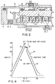
- Fig. 2 is a front elevational view in an enlarged scale and broken section of the heating chamber of the apparatus of the invention.
- Fig. 3 is a front elevational view, in cross section, illustrating another embodiment of the apparatus of the invention.
- Fig. 4 is a heating profile of temperature versus time that depicts typical heating cycle used by the apparatus and process of the invention.
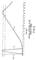
- Fig. 5 is another heating profile of temperature versus time that provides a comparison of the heat cycle associated with this invention, and a typical heat cycle associated with a belt furnace performing a similar reflow operation.
- the apparatus 10 for reflowing solder bonds has a container 12 having a stage 14 that supports substrate 16 above the floor 18 of container 12.
- the stage 14 can be pegs, fins, or any other suitable structure that engages the bottom surface of substrate 12 and maintains it at a predetermined height in the container.
- Devices 20 are shown positioned on and joined to substrate 16 with solder connections 22.
- fluid is pumped into container 12 through opening 24 to contact the bottom surface of substrate 16 to either heat or cool the substrate.
- the level of fluid is controlled by wier 26 as more clearly illustrated in Fig. 2.
- a cover 30 can be provided for container 12 to provide an inert gas atmosphere which can also be heated, for heating the devices 20 on substrate 16.
- the cover 30 has openings 32 and 34 for introducing and removing inert or heated gas to container 12. Any desirable gas can be introduced and exhausted through openings 32 and 34 including forming gas, hydrogen gas for flux free joining and inert gases.
- the various gases can be either heated, cooled, or at room temperature.
- a seal 36 positioned between the cover 30 and the top surface of substrate 16 confines the chosen environment to the surface area of the substrate and also keeps fluid and fluid vapor from contacting the top surface.
- another seal element 38 can be provided between the outer perimeter of cover 30 and container 12.
- the embodiment in Fig. 2 also includes an arrangement that provides support for pins 40 during the reflow heating cycle, when the pins are soldered or brazed on the substrate 16.
- the solder may soften during the heat cycle and stretch the solder securing them to the substrate.
- An apertured plate preferably of graphite, is supported in container 12. Openings 42 have a diameter greater than the diameter of pins 40.
- Openings 42 have a diameter greater than the diameter of pins 40.
- the fluid applies hydraulic pressure against the pins and has a frictional drag on the pins surface which exerts upward forces that aid in supporting the pins.
- Additional openings 44 can be provided to permit a greater rate of fluid flow.
- the pattern of the openings can be varied to achieve uniform heating of the substrate e.g., if corners lag then fewer holes are provided at the center of the substrate and more at the corners.
- any suitable fluid can be used in the practice of this invention.
- the fluid will be a liquid, such as oil or the like.
- the fluid must have a boiling point above the melting point of the solder material being reflowed and a relatively low vapor pressure as well as being non-explosive and non-toxic.
- the fluid should be sufficiently inert so that the surface of the substrate that it contacts is not degraded nor otherwise adversely affected. I have discovered that a suitable fluid is polyphenyl ether.
- a substrate temperature profile 46 consisting of a heat phase 48 where the substrate temperature increases at a rapid rate, a hold phase 50 where the substrate temperature is constant for a short time, and finally a cooling phase 52 where the substrate temperature is decreased rapidly.
- the fluid temperature profile 54 is maintained in container 12 by a mechanism to be described. Since there is a time lag between the substrate temperature and the fluid temperature.
- the profile 54 depicting fluid temperature therefore is several degrees higher than the substrate temperature as depicted by profile 46. Heating or cooling the substrate with liquid is much faster and more efficient than cooling with air or gas as a heating medium, or radiant heat.
- sump tank 60 receiving the fluid from container 12 that has overflowed wier 26 after coming in contact with substrate 16.
- the fluid is cooled and subsequently returned to holding tanks 62 and 64 where the temperature of the fluid is maintained, or the fluid heated.
- the fluid is stored at either a relatively low temperature for cooling purposes or a high temperature for heating purposes.
- Pumps 63 and 65 are provided in tanks 62 and 64, respectively, to supply the fluids, properly blended, to achieve the proper temperature to container 12.
- Valves 66 and 68 that control the flow of fluid from pumps 63 and 65 shift the flow from circulation within the tank to ensure uniformity of temperature throughout the tank to delivery to the processing containers.
- the computer controls the speed of the two pumps.
- Computer 70 is programmed to provide the proper blend of hot and cool liquids at the proper time to achieve an oil temperature profile, such as depicted in Fig. 4.
- the plumbing and the tanks are enclosed in a chamber 72 and a nitrogen environment maintained therein for safety.
- FIG. 3 there is depicted another preferred specific embodiment of the apparatus 80.
- Apparatus 80 does not have the capability of providing a closely controlled heating profile possible with apparatus 10.
- the apparatus is useful for removing devices 20 from substrates 16 for rework or for joining devices by manually placing and removing substrates on stage 14.
- the substrate 16 is accessible through opening 82 in glove box 84.
- Normally an inert gas environment is provided in glove box 84.
- Fluid is forced from the sump 60 into chamber 86 by pump 88.
- the fluid is forced upwardly through opening 24 into contact with the substrates 16.
- the fluid after overflowing wier 26 flows back to sump 60 and the process is repeated.
- a heating element 90 provides control of the fluid temperature.
- Fig. 5 of the drawing illustrates a heating profile 46 of the temperature on the top of ceramic substrate vs. time obtained by using the apparatus and process of this invention using a heated liquid, and subsequently a cooling liquid applied to the bottom surface of the substrate.
- comparison profile 56 vs. a plate of temperature on the top of the same ceramic substrate vs. time obtained with a belt furnace.
- the apparatus and method of the invention is particularly suited for solder bonding integrated circuit semiconductor devices to a ceramic substrate.
- the invention can be used for any application where it is advantageous to solder, braze, or otherwise bond elements to a workpiece without exposing the elements and/or the bond to elevated temperatures for lengthy periods of time or otherwise control the temperature for any reason.
- the invention is useful for bonding I/O pins, capacitors, attachment chips and the like to substrates of any material, and to remove and rebond elements where the assembly must be re-worked to correct for defects and the like.
- the environment on a surface of the substrate can be controlled to protect the elements to be bonded, or achieve conditions that are conducive to bonding integrity.
Landscapes
- Engineering & Computer Science (AREA)
- Mechanical Engineering (AREA)
- Electric Connection Of Electric Components To Printed Circuits (AREA)
- Wire Bonding (AREA)
Claims (15)
- Eine Vorrichtung (10) zum Neuaufschmelzen von Lötanschlüssen (22), die ein elektronisches Bauelement (20) mit einem Trägersubstrat (16) verbinden, enthaltend:
eine Stufe (14) zum Tragen des Substrates,
eine Fluidmenge, die auf eine Temperatur oberhalb des Schmelzpunktes des Lotes an den Lötanschlüssen erhitzbar ist,
eine Einrichtung zum Zuführen des Fluides zur Kontaktierung einer Oberfläche des Substrates (16) mit dem Fluid, wobei die Vorrichtung mit wenigstens einem Reservoir (62, 64) verbunden ist, und
Pumpenmittel (63, 65) zum Fördern der Flüssigkeit von dem Reservoir zum Kontakt mit einer Oberfläche, wobei die Vorrichtung dadurch gekennzeichnet ist, daß sie weiterhin enthält:
Mittel (66, 68, 70) zur Steuerung der Temperatur des Fluides, die in Kontakt mit dem Substrat gefördert wird, um anfangs die Temperatur des Fluides zu erhöhen und nachfolgend die Temperatur des Fluides zu verringern, wobei die Temperatur des Fluides, das in Kontakt mit dem Substrat ist, abhängig von der Steuereinrichtung geändert wird. - Die Vorrichtung von Anspruch 1, worin das elektronische Bauelement (2O) auf der oberen Oberfläche des Substrates (16) angeordnet ist und die Mittel zum Kontaktieren des Substrates mit Fluid die Bodenoberfläche des Substrates mit erhitztem Fluid kontaktieren.
- Die Vorrichtung von Anspruch 2, worin die Mittel zur Zufuhr von Fluid zur Kontaktierung des Substrates mit wenigstens zwei Fluidreservoiren (62, 64), die das Fluid bei unterschiedlichen Temperaturen bevorraten, einer Fluidpumpe (63, 65) und einem Mischventil (66, 68) verbunden sind, wobei die Steuervorrichtung die Fluidpumpen und die Mischventile (66, 68) steuert, um ein erhitztes Fluid mit sich ändernden Temperaturen zur Kontaktierung des Substrates zu fördern.
- Die Vorrichtung von Anspruch 3, worin das elektronische Bauteil ein integriertes Halbleiterbauteil ist, das eine Mehrzahl von Lötanschlüssen hat, die mit entsprechenden Lötkontakten auf der oberen Oberfläche des Substrates zu verbinden sind, und wobei das Substrat ein Mehrschichtkeramiksubstrat mit E/A-Anschlußstiften an der Bodenoberfläche ist.
- Die Vorrichtung von Anspruch 4, worin die Mittel zum Kontaktieren des Substrates mit Fluid weiterhin einen Behälter (12) aufweisen zum Aufnehmen und Tragen des Substrates darin in einer bestimmten Höhe, sowie ein Wehr (26) zum Aufrechterhalten des Pegels des Fluides in dem Behälter in einer Höhe, um den Kontakt des Fluides mit der Bodenoberfläche des Substrates aufrecht zu erhalten.
- Die Vorrichtung von Anspruch 5, die weiterhin eine Platte mit Öffnungen (42) aufweist zur Aufnahme der E/A-Anschlußstifte (40), wobei die Öffnungen eine Größe haben, um einen Freiraum zwischen den Stiften zu schaffen, so daß ein Fluidfluß zwischen der Öffnungswand und dem Anschlußstift ermöglicht ist, und wobei der Behälter ein Abdeckelement (30), ein Dichtelement (38) zwischen dem Abdeckelement und ein Substrat, das in dem Behälter gehalten ist, aufweist, so daß ein abgedichteter geschlossener Raum oberhalb der oberen Oberfläche des Bauteils, das auf der oberen Oberfläche angeordnet ist, geschaffen wird.
- Die Vorrichtung von Anspruch 6, worin Mittel (32, 34) vorgesehen sind, um ein Inertgas oder reduzierendes Gas in die abgeschlossene Umgebung einzubringen und in dieser zu zirkulieren.
- Die Vorrichtung von Anspruch 3, worin ein erstes Fluidreservoir (64) ein erhitztes Fluid und ein zweites Fluidreservoir (62) ein gekühltes Fluid beinhaltet, wobei die Steuervorrichtung so wirkt, daß Fluide von dem ersten Reservoir und dem zweiten Reservoir gemischt werden, um die Temperatur des Fluides, welches das Substrat kontaktiert, oberhalb des Schmelzpunktes des Lotes zu erhöhen und nachfolgend die Temperatur des Fluides, welches das Substrat kontaktiert, zu verringern, wobei ein Sammeltank (60) zur Aufnahme des Fluides, nachdem es das Substrat kontaktiert hat und eine Leitungsvorrichtung vorgesehen sind, um das Fluid von dem Sammeltank zu dem Fluidreservoir und dem zweiten Fluidreservoir zurückzuführen.
- Die Vorrichtung von Anspruch 8, worin eine Heizvorrichtung in jedem der ersten und zweiten Fluidreservoire vorgesehen ist und das Fluid Polyphenylether ist.
- Die Vorrichtung von Anspruch 1, worin das Reservoir in seiner Oberseite eine Öffnung aufweist (Fig. 3) und weiterhin aufweist:
eine Stütze zum Halten des Substrates oberhalb der Öffnung,
ein Wehr (26), das die Öffnung zum Aufrechterhalten eines Fluidpegels oberhalb der Bodenoberfläche eines Substrates umgibt, wenn dieses auf dem Träger angeordnet ist,
und einen Sammeltank zum Sammeln von Fluid, welches das Wehr überfließt,
eine Handschuhkammer (84) über dem Substrat,
und wobei:
die Pumpeneinrichtung Fluid von dem Sammeltank in das Fluidreservoir fördert,
das Fluid Polyphenyl-Äther ist,
ein Mittel vorgesehen ist, um eine Inertgas-Umgebung in der Handschuhkammer aufrecht zu erhalten,
ein Mittel vorgesehen ist, um das in die erhitzte Umgebung eingebrachte Gas zu erhitzen. - Die Vorrichtung von Anspruch 6, worin zusätzliche Öffnungen in der Platte vorgesehen sind, um zusätzliches Fluid in Richtung des Substrates zu fördern, um das Erreichen einer gleichförmigeren oberen Oberflächentemperatur des Substrates zu unterstützen.
- Ein Verfahren zum Neuaufschmelzen von Lötverbindungen, das ein elektronisches Bauteil mit einem Substrat verbindet, umfassend die folgenden Schritte:
Kontaktieren der Bodenoberfläche des Substrates mit einer zirkulierenden Flüssigkeit,
Steuern der Temperatur der Flüssigkeit, die in Kontakt mit dem Substrat gefördert wird, so daß die Temperatur der Flüssigkeit, die in Kontakt mit dem Substrat ist, geändert wird, umfassend:
Erhöhen der Temperatur der Flüssigkeit von einer Temperatur unterhalb des Schmelzpunktes des Lotes auf eine Temperatur, die den Schmelzpunkt des Lotmaterials der Lötanschlüsse überschreitet, und
nachfolgendes Absenken der Temperatur der Flüssigkeit auf eine Temperatur unterhalb des Schmelzpunktes des Lotmaterials,
wobei die Flüssigkeit in Richtung des Substrates von einem ersten und einem zweiten Tank fließt, wo die Temperatur oberhalb bzw. unterhalb der Lot-Schmelztemperatur gehalten ist. - Das Verfahren von Anspruch 12, worin das elektronische Bauteil ein integrierter Halbleiterbauteil ist, das eine Mehrzahl von Lötanschlüssen aufweist, die an seiner Unterseite verteilt sind und wobei das Substrat ein Mehrschichtkeramiksubstrat mit einer entsprechenden Mehrzahl von Lötanschlüssen auf seiner oberen Oberfläche ist.
- Das Verfahren von Anspruch 13, worin der gesamte Heiz- und Abkühlzyklus weniger als fünf Minuten dauert.
- Das Verfahren von Anspruch 12, worin das Lotmaterial der Verbindungen neu aufgeschmolzen wird, um elektrische Verbindungen herzustellen.
Applications Claiming Priority (2)
| Application Number | Priority Date | Filing Date | Title |
|---|---|---|---|
| US856516 | 1986-04-28 | ||
| US06/856,516 US4747533A (en) | 1986-04-28 | 1986-04-28 | Bonding method and apparatus |
Publications (3)
| Publication Number | Publication Date |
|---|---|
| EP0243621A2 EP0243621A2 (de) | 1987-11-04 |
| EP0243621A3 EP0243621A3 (en) | 1990-05-16 |
| EP0243621B1 true EP0243621B1 (de) | 1993-12-29 |
Family
ID=25323824
Family Applications (1)
| Application Number | Title | Priority Date | Filing Date |
|---|---|---|---|
| EP87103203A Expired - Lifetime EP0243621B1 (de) | 1986-04-28 | 1987-03-06 | Lötverfahren und Gerät |
Country Status (4)
| Country | Link |
|---|---|
| US (1) | US4747533A (de) |
| EP (1) | EP0243621B1 (de) |
| JP (1) | JPS62257737A (de) |
| DE (1) | DE3788589T2 (de) |
Families Citing this family (9)
| Publication number | Priority date | Publication date | Assignee | Title |
|---|---|---|---|---|
| US5102028A (en) * | 1990-04-02 | 1992-04-07 | International Business Machines Corporation | Localized soldering station using state changing medium |
| DE4024181C1 (en) * | 1990-07-30 | 1992-02-13 | Siemens Nixdorf Informationssysteme Ag, 4790 Paderborn, De | Vapour phase soldering installation - has valve in by=pass opening in dependence on preset temp. of sec. medium in soldering tank |
| JP4271299B2 (ja) * | 1999-06-28 | 2009-06-03 | 光洋サーモシステム株式会社 | リフロー炉 |
| EP1270130B1 (de) * | 2001-06-20 | 2010-03-24 | ALSTOM Technology Ltd | Lötverbindung und Verfahren zur Herstellung einer Lötverbindung |
| JP2007180447A (ja) * | 2005-12-28 | 2007-07-12 | Toyota Industries Corp | 半田付け方法、半田付け装置、及び半導体装置の製造方法 |
| JP4640170B2 (ja) * | 2005-12-28 | 2011-03-02 | 株式会社豊田自動織機 | 半田付け方法及び半導体モジュールの製造方法並びに半田付け装置 |
| JP4375491B1 (ja) * | 2008-06-23 | 2009-12-02 | 日本ジョイント株式会社 | 電子部品のはんだ付け装置およびはんだ付け方法 |
| US9166139B2 (en) * | 2009-05-14 | 2015-10-20 | The Neothermal Energy Company | Method for thermally cycling an object including a polarizable material |
| US11445650B2 (en) * | 2019-10-22 | 2022-09-13 | International Business Machines Corporation | Localized rework using liquid media soldering |
Family Cites Families (19)
| Publication number | Priority date | Publication date | Assignee | Title |
|---|---|---|---|---|
| US30399A (en) * | 1860-10-16 | Gas-kegttlatob | ||
| US3054174A (en) * | 1958-05-13 | 1962-09-18 | Rca Corp | Method for making semiconductor devices |
| US3825994A (en) * | 1972-11-15 | 1974-07-30 | Rca Corp | Method of soldering circuit components to a substrate |
| US4077467A (en) * | 1976-01-28 | 1978-03-07 | Spigarelli Donald J | Method and apparatus for soldering, fusing or brazing |
| US4055217A (en) * | 1976-02-02 | 1977-10-25 | Western Electric Company, Inc. | Method for maintaining a vapor blanket in a condensation heating facility |
| USRE30399E (en) | 1977-08-19 | 1980-09-09 | Western Electric Co., Inc. | Method for soldering, fusing or brazing |
| NL7805800A (nl) * | 1978-05-29 | 1979-12-03 | Philips Nv | Werkwijze en inrichting voor het solderen van onderde- len op een gatloos dikke-film substraat alsmede dikke-film substraat met onderdelen gesoldeerd met de werkwijze. |
| US4334646A (en) * | 1980-04-17 | 1982-06-15 | Harris Corporation | Method of solder reflow assembly |
| DE3040274C2 (de) * | 1980-10-23 | 1983-06-09 | ERSA Ernst Sachs KG, GmbH & Co, 6980 Wertheim | Vorrichtung zum Auslöten elektronischer Bauteile aus Leiterplatten |
| JPS57141993A (en) * | 1981-02-25 | 1982-09-02 | Matsushita Electric Industrial Co Ltd | Printed circuit board mounted with chip part and method of mounting chip part on printed circuit board |
| US4441647A (en) * | 1982-06-04 | 1984-04-10 | Northern Telecom Limited | Resoldering tool for ceramic substrate hybrid electronic circuits |
| US4474322A (en) * | 1982-11-12 | 1984-10-02 | Epe Corporation | Displacement soldering device |
| GB8312503D0 (en) * | 1983-05-06 | 1983-06-08 | Isc Chemicals Ltd | Vapour phase soldering |
| US4538757A (en) * | 1983-08-01 | 1985-09-03 | Motorola, Inc. | Wave soldering in a reducing atmosphere |
| FR2556083B1 (fr) * | 1983-10-11 | 1986-04-25 | Piezo Ceram Electronique | Machine perfectionnee de chauffage d'un article ou produit par condensation de vapeur sur celui-ci |
| US4561584A (en) * | 1983-10-17 | 1985-12-31 | Storage Technology Partners | Integrated circuit package removal |
| US4561586A (en) * | 1984-09-04 | 1985-12-31 | Burroughs Corporation | Method of removing a soldered integrated circuit package from a printed circuit board |
| US4580716A (en) * | 1984-10-17 | 1986-04-08 | Rca Corporation | Apparatus and method for vapor phase solder reflow |
| JPS6264475A (ja) * | 1985-09-17 | 1987-03-23 | Kenji Kondo | 物品の融着接合装置 |
-
1986
- 1986-04-28 US US06/856,516 patent/US4747533A/en not_active Expired - Fee Related
-
1987
- 1987-03-03 JP JP62046944A patent/JPS62257737A/ja active Granted
- 1987-03-06 DE DE3788589T patent/DE3788589T2/de not_active Expired - Fee Related
- 1987-03-06 EP EP87103203A patent/EP0243621B1/de not_active Expired - Lifetime
Also Published As
| Publication number | Publication date |
|---|---|
| EP0243621A2 (de) | 1987-11-04 |
| EP0243621A3 (en) | 1990-05-16 |
| JPS62257737A (ja) | 1987-11-10 |
| US4747533A (en) | 1988-05-31 |
| DE3788589D1 (de) | 1994-02-10 |
| DE3788589T2 (de) | 1994-06-30 |
| JPH0432542B2 (de) | 1992-05-29 |
Similar Documents
| Publication | Publication Date | Title |
|---|---|---|
| EP0918354B1 (de) | Methode zur Scheibenbereichsanordnung von Packungen in Chip-Grösse | |
| CN1066578C (zh) | 用于将集成电路芯片焊到芯片载体上的倒装片法 | |
| US5816473A (en) | Method of fabricating electronic circuit device and apparatus for performing the same method | |
| JP4759509B2 (ja) | はんだバンプ形成方法及び装置 | |
| US4334646A (en) | Method of solder reflow assembly | |
| EP0955676A2 (de) | Scheibenbereichsanordnung von Packungen in Chip-Grösse | |
| KR100669061B1 (ko) | 리플로 납땜 방법 | |
| US8925170B2 (en) | Method for removing an electronic component from a substrate | |
| US4747533A (en) | Bonding method and apparatus | |
| US20060065431A1 (en) | Self-reflowing printed circuit board and application methods | |
| EP0145975B1 (de) | Apparate und Verfahren zum Erhitzen von Gegenständen z.B. Chips während des Lötens und zum Halten der Temperatur der Gegenstände auf einem gewünschten Wert | |
| US6808958B2 (en) | Methods of bonding microelectronic elements | |
| CA2314036A1 (en) | Inert atmosphere soldering apparatus | |
| GB2353749A (en) | Reflow soldering apparatus and method | |
| RU2329624C2 (ru) | Способ и устройство для пайки оплавленным припоем с возможностью управления объемным потоком | |
| JP3718671B2 (ja) | フレキシブル基板上に電子部品を取付けるためのシステム及び方法 | |
| US5860582A (en) | Inert atmosphere soldering apparatus | |
| US4802276A (en) | Apparatus for printed wiring board component assembly | |
| US4805831A (en) | Bonding method | |
| CN101303989B (zh) | 焊料隆起形成方法及装置 | |
| JP2002373923A (ja) | 相互接続を除去する方法及び装置 | |
| JP3753524B2 (ja) | 電子部品の製造方法 | |
| US20260076244A1 (en) | Method and an apparatus for forming an electronic device | |
| JPH01289566A (ja) | ベーパーフェイズ・リフロー半田付装置 | |
| Pandey et al. | Thermal profile optimization for ceramic column grid array package assembly in selective reflow system for high reliability applications |
Legal Events
| Date | Code | Title | Description |
|---|---|---|---|
| PUAI | Public reference made under article 153(3) epc to a published international application that has entered the european phase |
Free format text: ORIGINAL CODE: 0009012 |
|
| AK | Designated contracting states |
Kind code of ref document: A2 Designated state(s): DE FR GB IT |
|
| 17P | Request for examination filed |
Effective date: 19880224 |
|
| PUAL | Search report despatched |
Free format text: ORIGINAL CODE: 0009013 |
|
| AK | Designated contracting states |
Kind code of ref document: A3 Designated state(s): DE FR GB IT |
|
| 17Q | First examination report despatched |
Effective date: 19910704 |
|
| GRAA | (expected) grant |
Free format text: ORIGINAL CODE: 0009210 |
|
| AK | Designated contracting states |
Kind code of ref document: B1 Designated state(s): DE FR GB IT |
|
| PG25 | Lapsed in a contracting state [announced via postgrant information from national office to epo] |
Ref country code: IT Free format text: LAPSE BECAUSE OF FAILURE TO SUBMIT A TRANSLATION OF THE DESCRIPTION OR TO PAY THE FEE WITHIN THE PRESCRIBED TIME-LIMIT;WARNING: LAPSES OF ITALIAN PATENTS WITH EFFECTIVE DATE BEFORE 2007 MAY HAVE OCCURRED AT ANY TIME BEFORE 2007. THE CORRECT EFFECTIVE DATE MAY BE DIFFERENT FROM THE ONE RECORDED. Effective date: 19931229 |
|
| REF | Corresponds to: |
Ref document number: 3788589 Country of ref document: DE Date of ref document: 19940210 |
|
| ET | Fr: translation filed | ||
| PLBE | No opposition filed within time limit |
Free format text: ORIGINAL CODE: 0009261 |
|
| STAA | Information on the status of an ep patent application or granted ep patent |
Free format text: STATUS: NO OPPOSITION FILED WITHIN TIME LIMIT |
|
| 26N | No opposition filed | ||
| PGFP | Annual fee paid to national office [announced via postgrant information from national office to epo] |
Ref country code: DE Payment date: 19950330 Year of fee payment: 9 |
|
| PGFP | Annual fee paid to national office [announced via postgrant information from national office to epo] |
Ref country code: FR Payment date: 19960307 Year of fee payment: 10 |
|
| PG25 | Lapsed in a contracting state [announced via postgrant information from national office to epo] |
Ref country code: DE Effective date: 19961203 |
|
| PGFP | Annual fee paid to national office [announced via postgrant information from national office to epo] |
Ref country code: GB Payment date: 19970224 Year of fee payment: 11 |
|
| PG25 | Lapsed in a contracting state [announced via postgrant information from national office to epo] |
Ref country code: FR Free format text: LAPSE BECAUSE OF NON-PAYMENT OF DUE FEES Effective date: 19971128 |
|
| REG | Reference to a national code |
Ref country code: FR Ref legal event code: ST |
|
| PG25 | Lapsed in a contracting state [announced via postgrant information from national office to epo] |
Ref country code: GB Free format text: LAPSE BECAUSE OF NON-PAYMENT OF DUE FEES Effective date: 19980306 |
|
| GBPC | Gb: european patent ceased through non-payment of renewal fee |
Effective date: 19980306 |