EP0246802A2 - Procédé pour nettoyer la surface d'un substrat semi-conducteur - Google Patents
Procédé pour nettoyer la surface d'un substrat semi-conducteur Download PDFInfo
- Publication number
- EP0246802A2 EP0246802A2 EP87304228A EP87304228A EP0246802A2 EP 0246802 A2 EP0246802 A2 EP 0246802A2 EP 87304228 A EP87304228 A EP 87304228A EP 87304228 A EP87304228 A EP 87304228A EP 0246802 A2 EP0246802 A2 EP 0246802A2
- Authority
- EP
- European Patent Office
- Prior art keywords
- substrate
- semiconductor substrate
- cleaning
- wet cleaning
- silicon
- Prior art date
- Legal status (The legal status is an assumption and is not a legal conclusion. Google has not performed a legal analysis and makes no representation as to the accuracy of the status listed.)
- Withdrawn
Links
Images

Classifications
-
- H—ELECTRICITY
- H10—SEMICONDUCTOR DEVICES; ELECTRIC SOLID-STATE DEVICES NOT OTHERWISE PROVIDED FOR
- H10P—GENERIC PROCESSES OR APPARATUS FOR THE MANUFACTURE OR TREATMENT OF DEVICES COVERED BY CLASS H10
- H10P70/00—Cleaning of wafers, substrates or parts of devices
- H10P70/10—Cleaning before device manufacture, i.e. Begin-Of-Line process
- H10P70/18—Cleaning before device manufacture, i.e. Begin-Of-Line process by combined dry cleaning and wet cleaning
-
- H—ELECTRICITY
- H10—SEMICONDUCTOR DEVICES; ELECTRIC SOLID-STATE DEVICES NOT OTHERWISE PROVIDED FOR
- H10P—GENERIC PROCESSES OR APPARATUS FOR THE MANUFACTURE OR TREATMENT OF DEVICES COVERED BY CLASS H10
- H10P50/00—Etching of wafers, substrates or parts of devices
- H10P50/20—Dry etching; Plasma etching; Reactive-ion etching
- H10P50/24—Dry etching; Plasma etching; Reactive-ion etching of semiconductor materials
- H10P50/242—Dry etching; Plasma etching; Reactive-ion etching of semiconductor materials of Group IV materials
Definitions
- the present invention relates to a process for treating a surface of a semiconductor substrate, more specifically, to a process for cleaning a surface of a semiconductor substrate for example prior to forming an epitaxial layer, a CVD layer a thermal oxide layer, a thermal nitride layer, or other film layer on the substrate.
- a more effective process for cleaning a surface of a semiconductor substrate in which the surface of the semiconductor substrate is preoxidized (also referred to as sacrifical oxidation) before wet cleaning as mentioned-above.
- This process comprises, for example, sequentially wet cleaning a substrate, oxidizing a surface of the substrate, removing the oxidized layer from the substrate, wet cleaning the surface of the substrate again, and forming a required layer on the surface of the substrate.
- this process is disadvantageous in that it involves many complicated steps, including the oxidation step.
- the heat treatment necessary for oxidation causes contaminants to diffuse into the semiconductor substrate, so that removal of the contaminants is made more difficult.
- an extremely thin layer such as a gate insulating layer of a MOS-VLSI is formed on the cleaned surface of the substrate, such remaining contaminants cause a deterioration of the extremely thin layer.
- An embodiment of the present invention may provide a process for treating a surface of a semiconductor substrate, which process permits an unimpaired layer to be formed on the treated surface of the substrate.
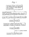
- a process for treating a surface of a semiconductor substrate comprising the steps of: etching a surface of the semiconductor in a atmosphere containing a free halogen or a halogen compound and irradiating at least one of the atmosphere above the semiconductor substrate and the surface of the semiconductor substrate with ultraviolet rays; and then wet cleaning the surface of the semiconductor substrate with a cleaning solution.
- a process for treating a surface of a silicon semiconductor substrate comprising the steps of: etching a surface of the silicon semiconductor substrate by placing the substrate in an atmosphere containing a free halogen or halogen compound and irradiating at least one of the atmosphere above the substrate and the surface of the semiconductor substrate with ultraviolet rays; rinsing the substrate; wet cleaning the surface of the substrate with an aqueous fluoric acid solution; rinsing the substrate; wet cleaning the surface of the substrate with an aqueous solution containing hydrogen peroxide and ammonia; and rinsing the substrate.
- reaction products formed from halogen and subst rate-constituting materials for example, silicon
- halogen and subst rate-constituting materials for example, silicon
- a p-type silicon substrate 2 for example, was placed on the susceptor 3 in chamber 1 and heated to about 100°C.
- High purity chlorine (Cl2) gas as an etching gas, was introduced from the chlorine container 9 into the chamber 1 and the chamber 1 evacuated to about 20 Torr.
- UV rays having a wavelength of 150 to 350 nm were irradiated toward the substrate 2 through the window 5 at a strength of 10 to 200 mW/cm2 for 1 to 5 minutes.
- This irradiation caused the chlorine gas to become excited and be brought to a radical state, and thus etch the surface of the silicon substrate 2 to a depth of 10 to 100 nm.
- the substrate 2 was then rinsed with running deionized water followed by immersion in boiling deionized water. Subsequently, the substrate was subjected to conventional wet solution cleaning, wherein first the substrate was wet cleaned with a 3% aqueous fluoric acid solution, rinsed with running deionized water and boiling deionized water, and then wet cleaned with an aqueous solution containing 22% hydrogen peroxide and 16% ammonia.
- the substrate was rinsed with running deionized water and then immersed in boiling deionized water.
- the cleaned surface of the silicon substrate was oxidized at 1000°C for 10 minutes to form a silicon dioxide layer having a thickness of 20 nm.
- the breakdown voltage of the silicon dioxide layer was 10.5 MV/cm.
- the same silicon substrate as above was subjected to the same wet solution cleaning as above, without a prior irradiationof UV rays in a halogen-containing atmosphere, and oxidized to form a silicon dioxide layer having a thickness of 20 nm.
- the breakdown voltage of this silicon dioxide layer was 9.5 MV/cm.
- the semiconductor substrate may be a compound semiconductor substrate.
- Other wet cleaning solutions for example, a solution containing hydrogen chloride and hydrogen peroxide (HCl ⁇ H2O2 ⁇ H2O) or nitric acid (HNO3) solution may be used.
Landscapes
- Cleaning Or Drying Semiconductors (AREA)
- Cleaning In General (AREA)
- Drying Of Semiconductors (AREA)
Applications Claiming Priority (2)
| Application Number | Priority Date | Filing Date | Title |
|---|---|---|---|
| JP61116423A JPS62272541A (ja) | 1986-05-20 | 1986-05-20 | 半導体基板の表面処理方法 |
| JP116423/86 | 1986-05-20 |
Publications (2)
| Publication Number | Publication Date |
|---|---|
| EP0246802A2 true EP0246802A2 (fr) | 1987-11-25 |
| EP0246802A3 EP0246802A3 (fr) | 1988-05-25 |
Family
ID=14686718
Family Applications (1)
| Application Number | Title | Priority Date | Filing Date |
|---|---|---|---|
| EP87304228A Withdrawn EP0246802A3 (fr) | 1986-05-20 | 1987-05-13 | Procédé pour nettoyer la surface d'un substrat semi-conducteur |
Country Status (3)
| Country | Link |
|---|---|
| EP (1) | EP0246802A3 (fr) |
| JP (1) | JPS62272541A (fr) |
| KR (1) | KR900004054B1 (fr) |
Cited By (8)
| Publication number | Priority date | Publication date | Assignee | Title |
|---|---|---|---|---|
| EP0316835A1 (fr) * | 1987-11-19 | 1989-05-24 | Oki Electric Industry Company, Limited | Méthode et dispositif pour nettoyer des substrats |
| EP0331555A1 (fr) * | 1988-02-26 | 1989-09-06 | Fujitsu Limited | Procédé de traitement gettering |
| WO1990007791A1 (fr) * | 1988-12-23 | 1990-07-12 | Eastman Kodak Company | Procede de nettoyage gazeux de dispositifs en silicium |
| US5225355A (en) * | 1988-02-26 | 1993-07-06 | Fujitsu Limited | Gettering treatment process |
| FR2703510A1 (fr) * | 1993-03-31 | 1994-10-07 | Fujitsu Ltd | Appareil et procédé de traitement de la surface d'une couche semiconductrice par plasma. |
| EP0758796A1 (fr) * | 1995-08-14 | 1997-02-19 | AT&T Corp. | Un procédé de fabrication d'un dispositif semi-conducteur |
| WO1998019336A1 (fr) * | 1996-10-31 | 1998-05-07 | Fsi International, Inc. | Traitement halogene/uv pour gravure par un oxyde anhydre |
| RU2195046C2 (ru) * | 2000-06-15 | 2002-12-20 | Акционерное общество открытого типа "НИИ молекулярной электроники и завод "Микрон" | Способ очистки поверхности |
Families Citing this family (5)
| Publication number | Priority date | Publication date | Assignee | Title |
|---|---|---|---|---|
| JPH0748482B2 (ja) * | 1989-10-14 | 1995-05-24 | 大日本スクリーン製造株式会社 | 酸化膜等の被膜除去処理後における基板表面の洗浄方法 |
| JP2853211B2 (ja) * | 1989-11-01 | 1999-02-03 | 富士通株式会社 | 半導体装置の製造方法 |
| JPH03211832A (ja) * | 1990-01-17 | 1991-09-17 | Fujitsu Ltd | 半導体装置の製造方法 |
| US6447604B1 (en) * | 2000-03-13 | 2002-09-10 | Advanced Technology Materials, Inc. | Method for achieving improved epitaxy quality (surface texture and defect density) on free-standing (aluminum, indium, gallium) nitride ((al,in,ga)n) substrates for opto-electronic and electronic devices |
| JP3341763B2 (ja) * | 2000-04-27 | 2002-11-05 | 住友電気工業株式会社 | 化合物半導体装置の製造方法および化合物半導体装置の製造装置 |
Family Cites Families (4)
| Publication number | Priority date | Publication date | Assignee | Title |
|---|---|---|---|---|
| US4264374A (en) * | 1978-09-25 | 1981-04-28 | International Business Machines Corporation | Cleaning process for p-type silicon surface |
| JPS58127328A (ja) * | 1982-01-26 | 1983-07-29 | Seiko Epson Corp | 半導体基板の絶縁保護膜の蝕刻方法 |
| JPS5986222A (ja) * | 1982-11-10 | 1984-05-18 | Toshiba Corp | ドライエツチング方法 |
| JPS59124124A (ja) * | 1982-12-29 | 1984-07-18 | Fujitsu Ltd | 半導体装置の製造方法 |
-
1986
- 1986-05-20 JP JP61116423A patent/JPS62272541A/ja active Pending
-
1987
- 1987-05-13 EP EP87304228A patent/EP0246802A3/fr not_active Withdrawn
- 1987-05-18 KR KR1019870004881A patent/KR900004054B1/ko not_active Expired
Cited By (13)
| Publication number | Priority date | Publication date | Assignee | Title |
|---|---|---|---|---|
| EP0316835A1 (fr) * | 1987-11-19 | 1989-05-24 | Oki Electric Industry Company, Limited | Méthode et dispositif pour nettoyer des substrats |
| US4871416A (en) * | 1987-11-19 | 1989-10-03 | Oki Electric Industry Co., Ltd. | Method and device for cleaning substrates |
| EP0331555A1 (fr) * | 1988-02-26 | 1989-09-06 | Fujitsu Limited | Procédé de traitement gettering |
| US5225355A (en) * | 1988-02-26 | 1993-07-06 | Fujitsu Limited | Gettering treatment process |
| WO1990007791A1 (fr) * | 1988-12-23 | 1990-07-12 | Eastman Kodak Company | Procede de nettoyage gazeux de dispositifs en silicium |
| US5919336A (en) * | 1993-03-31 | 1999-07-06 | Fujitsu Limited | Apparatus for fabricating semiconductor device and method for fabricating semiconductor device |
| FR2703510A1 (fr) * | 1993-03-31 | 1994-10-07 | Fujitsu Ltd | Appareil et procédé de traitement de la surface d'une couche semiconductrice par plasma. |
| US6024045A (en) * | 1993-03-31 | 2000-02-15 | Fujitsu Limited | Apparatus for fabricating semiconductor device and method for fabricating semiconductor device |
| EP0758796A1 (fr) * | 1995-08-14 | 1997-02-19 | AT&T Corp. | Un procédé de fabrication d'un dispositif semi-conducteur |
| US5814562A (en) * | 1995-08-14 | 1998-09-29 | Lucent Technologies Inc. | Process for semiconductor device fabrication |
| WO1998019336A1 (fr) * | 1996-10-31 | 1998-05-07 | Fsi International, Inc. | Traitement halogene/uv pour gravure par un oxyde anhydre |
| US5922219A (en) * | 1996-10-31 | 1999-07-13 | Fsi International, Inc. | UV/halogen treatment for dry oxide etching |
| RU2195046C2 (ru) * | 2000-06-15 | 2002-12-20 | Акционерное общество открытого типа "НИИ молекулярной электроники и завод "Микрон" | Способ очистки поверхности |
Also Published As
| Publication number | Publication date |
|---|---|
| JPS62272541A (ja) | 1987-11-26 |
| KR870011680A (ko) | 1987-12-26 |
| KR900004054B1 (ko) | 1990-06-09 |
| EP0246802A3 (fr) | 1988-05-25 |
Similar Documents
| Publication | Publication Date | Title |
|---|---|---|
| US5221423A (en) | Process for cleaning surface of semiconductor substrate | |
| US5534107A (en) | UV-enhanced dry stripping of silicon nitride films | |
| EP0688045A1 (fr) | Procédé de nettoyage | |
| US6692903B2 (en) | Substrate cleaning apparatus and method | |
| US5451547A (en) | Method of manufacturing semiconductor substrate | |
| KR100391840B1 (ko) | 반도체기판표면상의절연막형성방법및그형성장치 | |
| US5679171A (en) | Method of cleaning substrate | |
| US5516730A (en) | Pre-thermal treatment cleaning process of wafers | |
| WO1997013646A1 (fr) | Procede de nettoyage | |
| EP0246802A2 (fr) | Procédé pour nettoyer la surface d'un substrat semi-conducteur | |
| US5725677A (en) | Dry cleaning process for cleaning a surface | |
| Hattori et al. | Contamination Removal by Single‐Wafer Spin Cleaning with Repetitive Use of Ozonized Water and Dilute HF | |
| JPH06314679A (ja) | 半導体基板の洗浄方法 | |
| KR19990083236A (ko) | Al/Cu 금속라인상에서 포스트-RIE 폴리머를 제거하는 방법 | |
| KR970003887B1 (ko) | 집적 회로 어셈블리로부터 금속-함유 오염물질을 제거하기 위한 기체상 세정제 및 이를 사용하는 방법 | |
| EP0946978B1 (fr) | Traitement par irradiation et halogene pour gravure anhydrique d'un oxyde | |
| US6465374B1 (en) | Method of surface preparation | |
| JPH0496226A (ja) | 半導体装置の製造方法 | |
| EP1562226B1 (fr) | Procédé d'élimination d'oxydes d'une surface d'un substrat semiconducteur en Germanium | |
| JPH0536653A (ja) | 基板表面処理方法 | |
| JP2002543616A (ja) | 選択エッチングによるシリコンボディの欠陥の除去法 | |
| Meuris et al. | Cleaning technology for improved gate oxide integrity | |
| Butterbaugh et al. | Gas phase wafer cleaning technology | |
| JPS63117424A (ja) | 基板表面処理方法 | |
| JPH0821560B2 (ja) | 半導体装置の製造方法 |
Legal Events
| Date | Code | Title | Description |
|---|---|---|---|
| PUAI | Public reference made under article 153(3) epc to a published international application that has entered the european phase |
Free format text: ORIGINAL CODE: 0009012 |
|
| AK | Designated contracting states |
Kind code of ref document: A2 Designated state(s): DE FR GB |
|
| PUAL | Search report despatched |
Free format text: ORIGINAL CODE: 0009013 |
|
| AK | Designated contracting states |
Kind code of ref document: A3 Designated state(s): DE FR GB |
|
| 17P | Request for examination filed |
Effective date: 19880801 |
|
| 17Q | First examination report despatched |
Effective date: 19900404 |
|
| STAA | Information on the status of an ep patent application or granted ep patent |
Free format text: STATUS: THE APPLICATION HAS BEEN WITHDRAWN |
|
| 18W | Application withdrawn |
Withdrawal date: 19950828 |
|
| APAF | Appeal reference modified |
Free format text: ORIGINAL CODE: EPIDOSCREFNE |
|
| RIN1 | Information on inventor provided before grant (corrected) |
Inventor name: SUGINO, RINSHI Inventor name: ITO, TAKASHI |