EP0247603A2 - Eine Methode, um einen Photolack von einer Aluminiumlegierung zu entfernen - Google Patents
Eine Methode, um einen Photolack von einer Aluminiumlegierung zu entfernen Download PDFInfo
- Publication number
- EP0247603A2 EP0247603A2 EP87107743A EP87107743A EP0247603A2 EP 0247603 A2 EP0247603 A2 EP 0247603A2 EP 87107743 A EP87107743 A EP 87107743A EP 87107743 A EP87107743 A EP 87107743A EP 0247603 A2 EP0247603 A2 EP 0247603A2
- Authority
- EP
- European Patent Office
- Prior art keywords
- gas
- substrate
- aluminum alloy
- etching
- stripping
- Prior art date
- Legal status (The legal status is an assumption and is not a legal conclusion. Google has not performed a legal analysis and makes no representation as to the accuracy of the status listed.)
- Granted
Links
Images
Classifications
-
- H—ELECTRICITY
- H10—SEMICONDUCTOR DEVICES; ELECTRIC SOLID-STATE DEVICES NOT OTHERWISE PROVIDED FOR
- H10P—GENERIC PROCESSES OR APPARATUS FOR THE MANUFACTURE OR TREATMENT OF DEVICES COVERED BY CLASS H10
- H10P70/00—Cleaning of wafers, substrates or parts of devices
- H10P70/20—Cleaning during device manufacture
- H10P70/27—Cleaning during device manufacture during, before or after processing of conductive materials, e.g. polysilicon or amorphous silicon layers
- H10P70/273—Cleaning during device manufacture during, before or after processing of conductive materials, e.g. polysilicon or amorphous silicon layers the processing being a delineation of conductive layers, e.g. by RIE
-
- G—PHYSICS
- G03—PHOTOGRAPHY; CINEMATOGRAPHY; ANALOGOUS TECHNIQUES USING WAVES OTHER THAN OPTICAL WAVES; ELECTROGRAPHY; HOLOGRAPHY
- G03F—PHOTOMECHANICAL PRODUCTION OF TEXTURED OR PATTERNED SURFACES, e.g. FOR PRINTING, FOR PROCESSING OF SEMICONDUCTOR DEVICES; MATERIALS THEREFOR; ORIGINALS THEREFOR; APPARATUS SPECIALLY ADAPTED THEREFOR
- G03F7/00—Photomechanical, e.g. photolithographic, production of textured or patterned surfaces, e.g. printing surfaces; Materials therefor, e.g. comprising photoresists; Apparatus specially adapted therefor
- G03F7/26—Processing photosensitive materials; Apparatus therefor
- G03F7/42—Stripping or agents therefor
- G03F7/427—Stripping or agents therefor using plasma means only
-
- H—ELECTRICITY
- H10—SEMICONDUCTOR DEVICES; ELECTRIC SOLID-STATE DEVICES NOT OTHERWISE PROVIDED FOR
- H10P—GENERIC PROCESSES OR APPARATUS FOR THE MANUFACTURE OR TREATMENT OF DEVICES COVERED BY CLASS H10
- H10P50/00—Etching of wafers, substrates or parts of devices
- H10P50/20—Dry etching; Plasma etching; Reactive-ion etching
- H10P50/28—Dry etching; Plasma etching; Reactive-ion etching of insulating materials
- H10P50/286—Dry etching; Plasma etching; Reactive-ion etching of insulating materials of organic materials
- H10P50/287—Dry etching; Plasma etching; Reactive-ion etching of insulating materials of organic materials by chemical means
-
- G—PHYSICS
- G03—PHOTOGRAPHY; CINEMATOGRAPHY; ANALOGOUS TECHNIQUES USING WAVES OTHER THAN OPTICAL WAVES; ELECTROGRAPHY; HOLOGRAPHY
- G03F—PHOTOMECHANICAL PRODUCTION OF TEXTURED OR PATTERNED SURFACES, e.g. FOR PRINTING, FOR PROCESSING OF SEMICONDUCTOR DEVICES; MATERIALS THEREFOR; ORIGINALS THEREFOR; APPARATUS SPECIALLY ADAPTED THEREFOR
- G03F7/00—Photomechanical, e.g. photolithographic, production of textured or patterned surfaces, e.g. printing surfaces; Materials therefor, e.g. comprising photoresists; Apparatus specially adapted therefor
- G03F7/26—Processing photosensitive materials; Apparatus therefor
- G03F7/42—Stripping or agents therefor
Definitions
- This invention relates to a method for stripping a photo resist coated on a layer of an aluminum alloy, such as aluminum-copper, formed on a semiconductor substrate.
- Aluminum or aluminum-silicon alloy containing several percent of silicon has been generally used for an interconnection layer on a semiconductor device.
- the interconnection layer may be broken by electromigration, particularly in a semiconductor device where a very fine interconnection is required, such as 4 ⁇ m for a high speed ECL (Emitter Coupled Logic) or 1 ⁇ m for MOS (Metal Oxide Semiconductor), to achieve a greater density of integration, and a correspondingly higher density of the current flowing therethrough is required.
- ECL Electrode Coupled Logic
- MOS Metal Oxide Semiconductor
- an aluminum-copper alloy containing 2 to 4% of copper has come to be used, particularly where a high current-density is handled as in a bipolar device or a high-speed logic circuit.
- the aluminum-copper alloy suffers from problems due to residual chlorine therein.
- the HCl then reacts with the Al to produce AlCl3 again as follows: Al + 3 HCl ⁇ AlCl3 + 1 ⁇ 2 H2O.
- Al-Ti aluminum-titanium
- Al-Si aluminum-silicon
- the residual chlorine component on the substrate made of the above-mentioned aluminum or aluminum alloys can be removed, and thus the corrosion can be prevented.
- an aluminum alloy such as aluminum-copper (Al-Cu) or aluminum-copper-silicon (Al-Cu-Si) is etched, its chlorine component remains in the form of Cu x Cl y or a mixture of Cu, Cl, Al and carbon from the photo resist, which are difficult to remove as they have much higher sublimation temperatures than aluminum chloride, and may therefore cause corrosion even after the above-described chlorine-removal processing is carried out.
- a method for etching an aluminum alloy pattern on a semiconductor substrate comprises the steps of: forming a layer of aluminum alloy on a semiconductor substrate having an insulation layer thereon; forming a resist pattern on said aluminum alloy layer; etching an exposed portion of said aluminum alloy layer by the use of said resist pattern as a mask, whereby said aluminum alloy layer is patterned; stripping said resist pattern in an atmosphere containing a reactive species; and heating the substrate in a vacuum at a temperature higher than 100°C, whereby residual etching agent on the substrate is removed, said heating step being carried out concurrently with said stripping step or after said stripping step.
- the method includes the steps of: forming a layer of aluminum-copper alloy on a semiconductor substrate; forming a resist pattern on said alloy layer; etching said alloy layer by the use of said resist pattern in a chlorinated gas plasma so as to form an alloy pattern; downstream stripping said resist pattern in an atmosphere containing a reactive species; and heating the thus-processed substrate in a vacuum at a temperature higher than 100°C, to remove the residual chlorine component.
- the stripping process and the heating process may be combined; that is to say, be carried out concurrently.
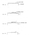
- Figs. 1(a) to 1(d) the fabrication steps in a preferred embodiment of the present invention are as follows:
- a semiconductor substrate 1 is fabricated with IC devices therein and coated with an insulation film thereon, for example of PSG (phospho silicate glass).
- a layer 2 of an aluminum-copper alloy, for example Al-Cu(4%) up to approximately 8000 ⁇ thick is formed all over the semiconductor substrate 1 by a known general method, such as sputtering, as shown in Fig. 1(a).
- a photo resist film is formed upon the alloy layer 2, and the resist film is patterned, as denoted by 3 in Fig. 1(b), by a known general lithography technique.
- the exposed portion of the alloy layer 2, i.e. the portion not masked by the photo resist pattern 3, is removed by a known general dry etching method.
- the dry etching may be a reactive ion etching method using as etching agent an etching gas such as a mixture of chlorine (Cl2) gas (24 sccm (standard cubic centimeter per minute)) and silicon tetrachloride (SiCl4) gas (40 sccm).
- etching gas such as a mixture of chlorine (Cl2) gas (24 sccm (standard cubic centimeter per minute)) and silicon tetrachloride (SiCl4) gas (40 sccm).
- the gas pressure is reduced to approximately 0.02 Torr (2.67 Pa), and radio frequency power of 13.56 MHz, for example, and 250 W, for example, is applied thereto for 5 minutes, for example, by well known methods.
- the etching gas is dissociated in a glow discharge driven by the applied radio frequency power and the chlorine atoms produced are active to react with the aluminum as well as the copper of the alloy.
- the aluminum chloride sublimes in the same manner as explained in the description of the prior art, and the copper chloride is sputtered by the energetic ion bombardment, so that the exposed portion of the alloy is etched and removed leaving the patterned layer 2 ⁇ , as shown in Fig. 1(c).
- the substrate 1 is transferred to a dry processing apparatus for stripping the patterned photo resist 3, passing through a vacuum system or an inert gas purged system, in order to avoid being exposed to the atmosphere. If the substrate is exposed to the atmosphere, the residual chlorine on the substrate reacts with water contained in the air and corrodes the alloy, as explained in the prior art.
- the patterned photo resist 3 on the patterned alloy layer 2 ⁇ is then stripped by a known downstream etching method.
- a stripping apparatus using microwave power which is preferably employed in this stripping step, and is also called a downstream ashing or an after-glow ashing, will be described in detail later.
- a reaction gas in the dry etching a mixture of a CF4 gas (100 sccm) and oxygen (O2) gas (1500 sccm), for example, is used at approximately 1 Torr (1.33 x 10² Pa), and microwave power of 2.45 GHz and 1 KW is applied thereto for 2 minutes, for example, while the substrate is kept at room temperature, such as 30°C.
- the substrate is heated so that the residual chlorine component is baked out.
- the heating is effected by the electric heater 31 built in the stage 25 to approximately 300°C for 2 minutes for example while the apparatus is pumped out to 0.2-0.3 Torr (0.27-0.4 x 10² Pa).
- the substrate is brought out of the apparatus, thus the processes of the invention are all finished.
- This method will be referred to as method I. It is also possible to heat the substrate on a separate heating stage from the stripping stage 25 in the vacuum chamber in order to save the cycle time for heating/cooling the massive stage.
- the last baking process of method I may be combined with the stripping process. In other words, these two processes can be carried out concurrently.
- the stripping process is carried out while the substrate 1 is heated to 200 to 300°C by an electric heater 31 mounted in the stage 25. This method will be referred to as method II.
- the etching gas may be a mixture of nitrogen (N2) gas (100 sccm) and oxygen (O2) gas (1500 sccm) at approximately 1 Torr (1.33 x 10² Pa), and the substrate may be heated at 200 to 300°C.
- N2 nitrogen
- O2 oxygen
- the combination of the heating and the downstream stripping is essential, because heating without stripping cannot remove the residual chlorine components under 400°C.
- conventional plasma stripping causes a particle problem by Al2O3 formation.
- the processed substrate was exposed to the atmosphere for 2 days.
- the alloy pattern was then optically observed to check for corrosion, and the residual chlorine atoms were measured by X-ray fluorescence spectroscopy.
- the check results are set out in the following table, in which
- the temperature must be lower than 400°C, and preferably be chosen between 250 and 300°C.
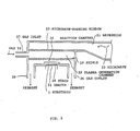
- the apparatus employs microwave power for producing reactive species as etching agent.
- the substrate 1 is loaded on the stage 25 in a reaction chamber 30.
- an electric heater 31 and a thermometer (not shown in the Figure) are mounted to heat the substrate when required.
- the chamber 30 is evacuated through gas outlets 26 by conventional evacuation equipment, which is not shown in the Figure.
- An etching gas is introduced into the chamber 30 through the gas inlet 27. By balancing the gas evacuation and gas introduction, the gas pressure within the chamber 30 is controlled to obtain the required gas pressure.
- Microwave power 22 is fed through the wave guide 21 and through the microwave-passing window 23 into the plasma generation chamber 29.
- the etching gas is made into plasma by the excitation by the microwave power.
- a reactive species, such as oxygen atoms, produced in the plasma comes out through the holes of the shield plate 28 and flows directly down on to the substrate 1, i.e.
- This reactive species is very reactive with the photo resist on the substrate, but does not harm the substrate by an ionic bombardment as in the plasma etching because the species coming out of the holes of the shield plate 28 is not ionic and no other ionic gas comes out at all. Therefore, this type of apparatus is advantageously employed for stripping the photo resist.
- aluminum-copper alloy is referred to in the above-described embodiment as the material to be processed, the present invention is also effective for other alloys such as AlCuSi and AlSiTiCu.
- etching gas for etching the alloy in the above-described embodiment
- gases of chlorine family such as BCl3, CCl4 and CHCl3, can be also used therein, as is well known.
- etching gas for stripping the photo resist in the above-described embodiment
- other fluorinated gases such as CHF3, C2F6, SF6, NF3 or CBrF3
- nitrogen-containing gases such as N2O or NO2
- a dry etching apparatus using a microwave frequency of 2.45 GHz is referred to in the above-described embodiment for stripping the photo resist
- other types of dry etching apparatus e.g. using a radio frequency of 13.56 MHz, can also be used, as is well known.
Landscapes
- Physics & Mathematics (AREA)
- Engineering & Computer Science (AREA)
- Plasma & Fusion (AREA)
- General Physics & Mathematics (AREA)
- Drying Of Semiconductors (AREA)
- ing And Chemical Polishing (AREA)
Applications Claiming Priority (3)
| Application Number | Priority Date | Filing Date | Title |
|---|---|---|---|
| JP12412386 | 1986-05-29 | ||
| JP61124123A JPS62281331A (ja) | 1986-05-29 | 1986-05-29 | エツチング方法 |
| JP124123/86 | 1986-05-29 |
Publications (3)
| Publication Number | Publication Date |
|---|---|
| EP0247603A2 true EP0247603A2 (de) | 1987-12-02 |
| EP0247603A3 EP0247603A3 (de) | 1988-07-20 |
| EP0247603B1 EP0247603B1 (de) | 1999-08-25 |
Family
ID=14877494
Family Applications (1)
| Application Number | Title | Priority Date | Filing Date |
|---|---|---|---|
| EP87107743A Expired - Lifetime EP0247603B1 (de) | 1986-05-29 | 1987-05-27 | Eine Methode, um einen Photolack von einer Aluminiumlegierung zu entfernen |
Country Status (5)
| Country | Link |
|---|---|
| US (2) | US6184148B1 (de) |
| EP (1) | EP0247603B1 (de) |
| JP (1) | JPS62281331A (de) |
| KR (2) | KR900004053B1 (de) |
| DE (1) | DE3752290T2 (de) |
Cited By (12)
| Publication number | Priority date | Publication date | Assignee | Title |
|---|---|---|---|---|
| EP0416774A1 (de) * | 1989-08-28 | 1991-03-13 | Hitachi, Ltd. | Verfahren zur Behandlung eines Aluminium enthaltenden Musters |
| DE4040061A1 (de) * | 1990-07-04 | 1992-01-23 | Mitsubishi Electric Corp | Verfahren zur herstellung einer strukturierten verbindungsschicht |
| EP0485802A1 (de) * | 1990-10-30 | 1992-05-20 | Nec Corporation | Verfahren zur Korrosionsverhinderung von Aluminiumlegierungen |
| FR2720854A1 (fr) * | 1993-12-28 | 1995-12-08 | Fujitsu Ltd | Procédé de fabrication de dispositifs à semiconducteurs dotés d'un câblage en aluminium par gravure et chauffage sous vide. |
| EP0651437A3 (de) * | 1993-10-29 | 1996-04-17 | Applied Materials Inc | Plasma-Ätzverfahren. |
| EP0709877A4 (de) * | 1993-05-20 | 1997-11-26 | Hitachi Ltd | Verfahren für plasma-behandlung |
| US5868854A (en) * | 1989-02-27 | 1999-02-09 | Hitachi, Ltd. | Method and apparatus for processing samples |
| WO1999004606A3 (en) * | 1997-07-14 | 1999-04-22 | Lam Res Corp | Compact microwave downstream plasma system |
| GB2339494A (en) * | 1998-07-09 | 2000-01-26 | Nec Corp | Patterning conductive lines without after-corrosion |
| US6060397A (en) * | 1995-07-14 | 2000-05-09 | Applied Materials, Inc. | Gas chemistry for improved in-situ cleaning of residue for a CVD apparatus |
| US6077788A (en) * | 1989-02-27 | 2000-06-20 | Hitachi, Ltd. | Method and apparatus for processing samples |
| US6989228B2 (en) | 1989-02-27 | 2006-01-24 | Hitachi, Ltd | Method and apparatus for processing samples |
Families Citing this family (12)
| Publication number | Priority date | Publication date | Assignee | Title |
|---|---|---|---|---|
| JP2728483B2 (ja) * | 1989-02-01 | 1998-03-18 | 株式会社日立製作所 | 試料後処理方法と装置 |
| US6451217B1 (en) * | 1998-06-09 | 2002-09-17 | Speedfam-Ipec Co., Ltd. | Wafer etching method |
| US20050022839A1 (en) * | 1999-10-20 | 2005-02-03 | Savas Stephen E. | Systems and methods for photoresist strip and residue treatment in integrated circuit manufacturing |
| US6660646B1 (en) * | 2000-09-21 | 2003-12-09 | Northrop Grumman Corporation | Method for plasma hardening photoresist in etching of semiconductor and superconductor films |
| US20020142612A1 (en) * | 2001-03-30 | 2002-10-03 | Han-Ming Wu | Shielding plate in plasma for uniformity improvement |
| KR100928098B1 (ko) * | 2002-12-24 | 2009-11-24 | 동부일렉트로닉스 주식회사 | 산화막을 이용한 메탈라인 형성방법 |
| US20070186953A1 (en) * | 2004-07-12 | 2007-08-16 | Savas Stephen E | Systems and Methods for Photoresist Strip and Residue Treatment in Integrated Circuit Manufacturing |
| KR100734778B1 (ko) | 2005-08-25 | 2007-07-03 | 세메스 주식회사 | 플라즈마를 이용한 기판 처리 장치 및 방법 |
| US20080061112A1 (en) * | 2006-09-07 | 2008-03-13 | Shih-Ju Liang | Method for soldering charge coupled device and tooling thereof |
| CN102226635B (zh) * | 2011-06-09 | 2013-02-27 | 四川宏普微波科技有限公司 | 一种微波连续冻干装置 |
| CN102929110B (zh) * | 2012-11-06 | 2014-03-19 | 中国科学院微电子研究所 | 一种微波激发的超临界干燥装置及方法 |
| US10866516B2 (en) | 2016-08-05 | 2020-12-15 | Taiwan Semiconductor Manufacturing Co., Ltd. | Metal-compound-removing solvent and method in lithography |
Family Cites Families (17)
| Publication number | Priority date | Publication date | Assignee | Title |
|---|---|---|---|---|
| JPS53112065A (en) * | 1977-03-11 | 1978-09-30 | Toshiba Corp | Removing method of high molecular compound |
| US4183781A (en) * | 1978-09-25 | 1980-01-15 | International Business Machines Corporation | Stabilization process for aluminum microcircuits which have been reactive-ion etched |
| JPS5852324B2 (ja) * | 1979-10-11 | 1983-11-22 | 富士通株式会社 | 半導体装置の製造方法 |
| JPS57170534A (en) * | 1981-04-15 | 1982-10-20 | Hitachi Ltd | Dry etching method for aluminum and aluminum alloy |
| US4370195A (en) * | 1982-03-25 | 1983-01-25 | Rca Corporation | Removal of plasma etching residues |
| US4718976A (en) * | 1982-03-31 | 1988-01-12 | Fujitsu Limited | Process and apparatus for plasma treatment |
| JPS593927A (ja) | 1982-06-29 | 1984-01-10 | Fujitsu Ltd | 薄膜のエツチング方法 |
| JPS59186326A (ja) | 1983-04-06 | 1984-10-23 | Hitachi Ltd | プラズマ処理装置 |
| JPS59210644A (ja) * | 1983-05-16 | 1984-11-29 | Oki Electric Ind Co Ltd | 半導体装置の製造方法 |
| JPS6016424A (ja) * | 1983-07-08 | 1985-01-28 | Fujitsu Ltd | マイクロ波プラズマ処理方法及びその装置 |
| JPS6130036A (ja) * | 1984-07-23 | 1986-02-12 | Fujitsu Ltd | マイクロ波プラズマ処理装置 |
| US4592800A (en) * | 1984-11-02 | 1986-06-03 | Oerlikon-Buhrle U.S.A. Inc. | Method of inhibiting corrosion after aluminum etching |
| US4631105A (en) * | 1985-04-22 | 1986-12-23 | Branson International Plasma Corporation | Plasma etching apparatus |
| US4699689A (en) * | 1985-05-17 | 1987-10-13 | Emergent Technologies Corporation | Method and apparatus for dry processing of substrates |
| JPH0722153B2 (ja) * | 1985-09-09 | 1995-03-08 | 日本電信電話株式会社 | ドライエツチング方法および装置 |
| US4632719A (en) * | 1985-09-18 | 1986-12-30 | Varian Associates, Inc. | Semiconductor etching apparatus with magnetic array and vertical shield |
| US4662977A (en) * | 1986-05-05 | 1987-05-05 | University Patents, Inc. | Neutral particle surface alteration |
-
1986
- 1986-05-29 JP JP61124123A patent/JPS62281331A/ja active Granted
-
1987
- 1987-05-27 EP EP87107743A patent/EP0247603B1/de not_active Expired - Lifetime
- 1987-05-27 DE DE3752290T patent/DE3752290T2/de not_active Expired - Fee Related
- 1987-05-29 KR KR1019870005360A patent/KR900004053B1/ko not_active Expired
- 1987-05-29 KR KR1019870005360A patent/KR870011678A/ko active Granted
-
1997
- 1997-04-18 US US08/839,371 patent/US6184148B1/en not_active Expired - Fee Related
-
2000
- 2000-08-16 US US09/639,113 patent/US6486073B1/en not_active Expired - Fee Related
Cited By (23)
| Publication number | Priority date | Publication date | Assignee | Title |
|---|---|---|---|---|
| US7132293B2 (en) | 1989-02-27 | 2006-11-07 | Hitachi, Ltd. | Method and apparatus for processing samples |
| US6537415B2 (en) | 1989-02-27 | 2003-03-25 | Hitachi, Ltd. | Apparatus for processing samples |
| US6254721B1 (en) | 1989-02-27 | 2001-07-03 | Hitachi, Ltd. | Method and apparatus for processing samples |
| US6077788A (en) * | 1989-02-27 | 2000-06-20 | Hitachi, Ltd. | Method and apparatus for processing samples |
| US6537417B2 (en) | 1989-02-27 | 2003-03-25 | Hitachi, Ltd. | Apparatus for processing samples |
| US6656846B2 (en) | 1989-02-27 | 2003-12-02 | Hitachi, Ltd. | Apparatus for processing samples |
| US6036816A (en) * | 1989-02-27 | 2000-03-14 | Hitachi, Ltd. | Apparatus for processing a sample having a metal laminate |
| US6989228B2 (en) | 1989-02-27 | 2006-01-24 | Hitachi, Ltd | Method and apparatus for processing samples |
| US5952245A (en) * | 1989-02-27 | 1999-09-14 | Hitachi, Ltd. | Method for processing samples |
| US5868854A (en) * | 1989-02-27 | 1999-02-09 | Hitachi, Ltd. | Method and apparatus for processing samples |
| US5380397A (en) * | 1989-08-28 | 1995-01-10 | Hitachi, Ltd. | Method of treating samples |
| US5556714A (en) * | 1989-08-28 | 1996-09-17 | Hitachi, Ltd. | Method of treating samples |
| EP0416774A1 (de) * | 1989-08-28 | 1991-03-13 | Hitachi, Ltd. | Verfahren zur Behandlung eines Aluminium enthaltenden Musters |
| US6329298B1 (en) | 1989-08-28 | 2001-12-11 | Hitachi, Ltd. | Apparatus for treating samples |
| US5198388A (en) * | 1990-07-04 | 1993-03-30 | Mitsubishi Denki Kabushiki Kaisha | Method of forming interconnection patterns |
| DE4040061A1 (de) * | 1990-07-04 | 1992-01-23 | Mitsubishi Electric Corp | Verfahren zur herstellung einer strukturierten verbindungsschicht |
| EP0485802A1 (de) * | 1990-10-30 | 1992-05-20 | Nec Corporation | Verfahren zur Korrosionsverhinderung von Aluminiumlegierungen |
| EP0709877A4 (de) * | 1993-05-20 | 1997-11-26 | Hitachi Ltd | Verfahren für plasma-behandlung |
| EP0651437A3 (de) * | 1993-10-29 | 1996-04-17 | Applied Materials Inc | Plasma-Ätzverfahren. |
| FR2720854A1 (fr) * | 1993-12-28 | 1995-12-08 | Fujitsu Ltd | Procédé de fabrication de dispositifs à semiconducteurs dotés d'un câblage en aluminium par gravure et chauffage sous vide. |
| US6060397A (en) * | 1995-07-14 | 2000-05-09 | Applied Materials, Inc. | Gas chemistry for improved in-situ cleaning of residue for a CVD apparatus |
| WO1999004606A3 (en) * | 1997-07-14 | 1999-04-22 | Lam Res Corp | Compact microwave downstream plasma system |
| GB2339494A (en) * | 1998-07-09 | 2000-01-26 | Nec Corp | Patterning conductive lines without after-corrosion |
Also Published As
| Publication number | Publication date |
|---|---|
| KR870011678A (ko) | 1987-12-26 |
| JPH057862B2 (de) | 1993-01-29 |
| EP0247603A3 (de) | 1988-07-20 |
| US6184148B1 (en) | 2001-02-06 |
| DE3752290T2 (de) | 2000-01-27 |
| KR900004053B1 (ko) | 1990-06-09 |
| US6486073B1 (en) | 2002-11-26 |
| JPS62281331A (ja) | 1987-12-07 |
| EP0247603B1 (de) | 1999-08-25 |
| DE3752290D1 (de) | 1999-09-30 |
Similar Documents
| Publication | Publication Date | Title |
|---|---|---|
| EP0247603A2 (de) | Eine Methode, um einen Photolack von einer Aluminiumlegierung zu entfernen | |
| US4028155A (en) | Process and material for manufacturing thin film integrated circuits | |
| US4547260A (en) | Process for fabricating a wiring layer of aluminum or aluminum alloy on semiconductor devices | |
| EP0416774B1 (de) | Verfahren zur Behandlung eines Aluminium enthaltenden Musters | |
| US6589890B2 (en) | Precleaning process for metal plug that minimizes damage to low-κ dielectric | |
| JP3090476B2 (ja) | プラズマ化学蒸着を用いてフッ化シリコン酸化物層を形成する方法 | |
| EP0489179B1 (de) | Verfahren zum herstellen eines integrierten halbleiterschaltkreises | |
| KR100255960B1 (ko) | 질화 실리콘막의 uv-촉진된 건식 스트리핑 방법 | |
| US7202176B1 (en) | Enhanced stripping of low-k films using downstream gas mixing | |
| US4938839A (en) | Method of removing photoresist on a semiconductor wafer | |
| EP0047002A2 (de) | Plasma-Ätzvorrichtung | |
| EP0019915B1 (de) | Verfahren zur Korrosionsverhinderung von Aluminium und Aluminiumlegierungen | |
| GB2080737A (en) | Plasma passivation of plasma-etched aluminium films | |
| JP2000012514A (ja) | 後処理方法 | |
| US4229247A (en) | Glow discharge etching process for chromium | |
| US5211804A (en) | Method for dry etching | |
| US6162733A (en) | Method for removing contaminants from integrated circuits | |
| KR950005351B1 (ko) | 알루미늄 합금의 부식 방지 방법 | |
| JPH0793293B2 (ja) | 後処理方法 | |
| Jimbo et al. | Resist and Sidewall Film Removal after Al Reactive Ion Etching (RIE) Employing F+ H2O Downstream Ashing | |
| JPH04316327A (ja) | ドライエッチング装置及びチャンバの洗浄方法 | |
| JPH0472082A (ja) | ドライエッチング方法 | |
| Voshchenkov | PLASMA ETCHING PROCESSES FOR GIGAHERTZ SILICON INTEGRATED CIRCUITS (Part 2) | |
| JPH0855838A (ja) | 微細加工装置のクリーニング方法 | |
| JPH07201813A (ja) | 半導体装置の製造方法およびその製造装置 |
Legal Events
| Date | Code | Title | Description |
|---|---|---|---|
| PUAI | Public reference made under article 153(3) epc to a published international application that has entered the european phase |
Free format text: ORIGINAL CODE: 0009012 |
|
| AK | Designated contracting states |
Kind code of ref document: A2 Designated state(s): DE FR GB |
|
| PUAL | Search report despatched |
Free format text: ORIGINAL CODE: 0009013 |
|
| AK | Designated contracting states |
Kind code of ref document: A3 Designated state(s): DE FR GB |
|
| 17P | Request for examination filed |
Effective date: 19881209 |
|
| 17Q | First examination report despatched |
Effective date: 19910625 |
|
| APAB | Appeal dossier modified |
Free format text: ORIGINAL CODE: EPIDOS NOAPE |
|
| GRAG | Despatch of communication of intention to grant |
Free format text: ORIGINAL CODE: EPIDOS AGRA |
|
| GRAH | Despatch of communication of intention to grant a patent |
Free format text: ORIGINAL CODE: EPIDOS IGRA |
|
| GRAG | Despatch of communication of intention to grant |
Free format text: ORIGINAL CODE: EPIDOS AGRA |
|
| GRAH | Despatch of communication of intention to grant a patent |
Free format text: ORIGINAL CODE: EPIDOS IGRA |
|
| GRAG | Despatch of communication of intention to grant |
Free format text: ORIGINAL CODE: EPIDOS AGRA |
|
| GRAG | Despatch of communication of intention to grant |
Free format text: ORIGINAL CODE: EPIDOS AGRA |
|
| GRAH | Despatch of communication of intention to grant a patent |
Free format text: ORIGINAL CODE: EPIDOS IGRA |
|
| GRAG | Despatch of communication of intention to grant |
Free format text: ORIGINAL CODE: EPIDOS AGRA |
|
| GRAH | Despatch of communication of intention to grant a patent |
Free format text: ORIGINAL CODE: EPIDOS IGRA |
|
| GRAH | Despatch of communication of intention to grant a patent |
Free format text: ORIGINAL CODE: EPIDOS IGRA |
|
| GRAA | (expected) grant |
Free format text: ORIGINAL CODE: 0009210 |
|
| AK | Designated contracting states |
Kind code of ref document: B1 Designated state(s): DE FR GB |
|
| REF | Corresponds to: |
Ref document number: 3752290 Country of ref document: DE Date of ref document: 19990930 |
|
| ET | Fr: translation filed | ||
| PLBE | No opposition filed within time limit |
Free format text: ORIGINAL CODE: 0009261 |
|
| STAA | Information on the status of an ep patent application or granted ep patent |
Free format text: STATUS: NO OPPOSITION FILED WITHIN TIME LIMIT |
|
| 26N | No opposition filed | ||
| REG | Reference to a national code |
Ref country code: GB Ref legal event code: IF02 |
|
| PGFP | Annual fee paid to national office [announced via postgrant information from national office to epo] |
Ref country code: FR Payment date: 20050511 Year of fee payment: 19 |
|
| PGFP | Annual fee paid to national office [announced via postgrant information from national office to epo] |
Ref country code: DE Payment date: 20050519 Year of fee payment: 19 |
|
| PGFP | Annual fee paid to national office [announced via postgrant information from national office to epo] |
Ref country code: GB Payment date: 20050525 Year of fee payment: 19 |
|
| APAH | Appeal reference modified |
Free format text: ORIGINAL CODE: EPIDOSCREFNO |
|
| PG25 | Lapsed in a contracting state [announced via postgrant information from national office to epo] |
Ref country code: GB Free format text: LAPSE BECAUSE OF NON-PAYMENT OF DUE FEES Effective date: 20060527 |
|
| PG25 | Lapsed in a contracting state [announced via postgrant information from national office to epo] |
Ref country code: DE Free format text: LAPSE BECAUSE OF NON-PAYMENT OF DUE FEES Effective date: 20061201 |
|
| GBPC | Gb: european patent ceased through non-payment of renewal fee |
Effective date: 20060527 |
|
| REG | Reference to a national code |
Ref country code: FR Ref legal event code: ST Effective date: 20070131 |
|
| PG25 | Lapsed in a contracting state [announced via postgrant information from national office to epo] |
Ref country code: FR Free format text: LAPSE BECAUSE OF NON-PAYMENT OF DUE FEES Effective date: 20060531 |