EP0250152A2 - Circuit de transformation - Google Patents
Circuit de transformation Download PDFInfo
- Publication number
- EP0250152A2 EP0250152A2 EP87305110A EP87305110A EP0250152A2 EP 0250152 A2 EP0250152 A2 EP 0250152A2 EP 87305110 A EP87305110 A EP 87305110A EP 87305110 A EP87305110 A EP 87305110A EP 0250152 A2 EP0250152 A2 EP 0250152A2
- Authority
- EP
- European Patent Office
- Prior art keywords
- signals
- transform
- circuit
- multipliers
- responsive
- Prior art date
- Legal status (The legal status is an assumption and is not a legal conclusion. Google has not performed a legal analysis and makes no representation as to the accuracy of the status listed.)
- Granted
Links
Images


Classifications
-
- G—PHYSICS
- G06—COMPUTING OR CALCULATING; COUNTING
- G06T—IMAGE DATA PROCESSING OR GENERATION, IN GENERAL
- G06T1/00—General purpose image data processing
-
- H—ELECTRICITY
- H04—ELECTRIC COMMUNICATION TECHNIQUE
- H04N—PICTORIAL COMMUNICATION, e.g. TELEVISION
- H04N19/00—Methods or arrangements for coding, decoding, compressing or decompressing digital video signals
- H04N19/60—Methods or arrangements for coding, decoding, compressing or decompressing digital video signals using transform coding
-
- G—PHYSICS
- G06—COMPUTING OR CALCULATING; COUNTING
- G06F—ELECTRIC DIGITAL DATA PROCESSING
- G06F17/00—Digital computing or data processing equipment or methods, specially adapted for specific functions
- G06F17/10—Complex mathematical operations
- G06F17/14—Fourier, Walsh or analogous domain transformations, e.g. Laplace, Hilbert, Karhunen-Loeve, transforms
- G06F17/147—Discrete orthonormal transforms, e.g. discrete cosine transform, discrete sine transform, and variations therefrom, e.g. modified discrete cosine transform, integer transforms approximating the discrete cosine transform
Definitions
- This relates to data processing apparatus for encoding and decoding two-dimensional information in an efficient manner. More particularly, this relates to apparatus for the creation of a two-dimensional cosine transform and its inverse.
- Image data compression has been a topic of considerable interest in recent years because of the burgeoning fields of information and communication. Compression of image data is necessary because in order to achieve pleasing results a picture must contain a large number of pixels, or elemental picture elements. Such images, however, contain a large amount of redundant information.
- researchers have tried to encode images in a number of ways to reduce this redundancy and to thereby realize transmission and storage savings. These encoding approaches can be broadly divided into pulse code modulation, interpolative or extrapolative coding, vector quantization, and transform coding.
- DPCM differential pulse code modulation
- an image block is decomposed into a set of vectors. From the possible signal patterns and corresponding vectors, a subset of representative vectors is selected and included in a code book. When encoding, the developed sets of vectors are replaced with the closest representative vectors in the code book, and compression is achieved by further replacing the representative vectors with labels.
- transform coding instead of coding the image as discrete intensity values of sampling points, an alternative representation is made first by transforming blocks of pixels into a set of coefficients. It is the coefficients that are quantized and transmitted.
- transformations such as the Hadamard, the Karhunen-Loeve, and the Discrete Cosine Transforms. These transforms conserve the signal energy in the transform domain but, typically, most of the energy is concentrated in relatively few samples. Samples that are very close to zero need not be transmitted, and samples of relatively low value can be quantized coarsely. This results in substantial compression of the data that needs to be either stored or transmitted. Huffman coding is often used after quantizing to further reduce the transmission rate.
- the Discrete Cosine Transform is a commonly applied transform. It is usually realized with processors built from TTL or ECL hardware which processes video at rates of about 8-10 megasamples per second.
- the transformation consists of multiplying an -n x n matrix by an n element vector. Since parallel hardware multipliers are expensive, most theoretical work has concentrated on exploiting the symmetries of the cosine matrix to partition it into smaller matrices, so that the total number of multiplications is reduced. This results in a variety of "Fast Discrete Cosine Transform" algorithms, which are close cousins of the FFT.
- R. L. Wilhelm describes a multiple point discrete transform processor in U.S. Patent 4,449,194, issued May 15, 1984.
- the Wilhelm processor approximates each term of the Discrete Cosine Transform by power of 2 terms so that all mathematical steps are performed by shifting and/or subtracting digital signals.
- symmetries of the cosine matrix of coefficients are utilized to allow all multiplications to be done by "constant multipliers" comprising combinations of look-up tables and adders.
- Transform coefficients are developed by dividing each into a sequence of blocks of preselected size, the information in the blocks is sorted to develop a specific order and the reordered blocks are applied seriatim to a first one-dimensional cosine transform circuit employing the constant multipliers.
- the output of the first cosine transform circuit is applied to a transposing memory and then to a second cosine transform circuit that also employs "constant multipliers". Both the direct discrete cosine transform and the inverse discrete cosine transform are accomplished in this manner, and in one illustrative implementation both transforms are generated with the same constant multipliers and essentially the same support circuitry.
- Transform coding is usually applied as an intraframe coding technique which eliminates the redundancy in each single frame of video.
- the picture is divided into blocks of size n x n (n pixels x n lines) where n is a power of 2 and is usually 8, 16 or 32.
- the transform operation is applied to each block, and its results replace the pixel values (local information) with n 2 transform coefficients (block-wide information).
- Each of the transform coefficients says something about the entire block.
- the "DC coefficient" represents the average value of the pixels in the block.
- Other coefficients represent the extent to which certain two-dimensional spatial frequency patterns are present in the block. Because the cosine vector set is orthogonal, information in one coefficient cannot be represented by any any combination of the others.
- Compression is achieved by discarding a number of coefficients (replacing them by zero at the decoder) and by restricting others to a smaller or coarser range of values. This approach works well because most of the information in the picture is contained in the low spatial frequency patterns, and the high frequency patterns have values close to zero. The eye is unlikely to miss the high frequency information that is thrown away.
- Huffman coding is often used to reduce the transmission rate still further. Rare large values of high spatial frequency coefficients are given long codes while values at or near zero are given have very short codes.
- FIG. 1 is a the block diagram of a 16 x 16 transform processor with m bit words.
- m ranges from 12 to 16 to avoid round-off errors. If compression is high, quantization error will be high and 12 bit accuracy will be sufficient. For more modest compression and higher quality, 14 to 16 bits is more appropriate.
- an initial 16 line "block reordering memory" 10 is used to rearrange each block of 16 raster scanned lines into blocks of 16 by 16, or 256 pels. It also serves the function of reordering the samples in each block in accordance with a preselected reordering pattern. One such pattern is described below.
- the output of memory 10 is applied to a one-dimensional transform circuit 20; the output of transform circuit 20 is applied to a "scan transpose" memory 30; and the output of memory 30 is applied to a second one-dimensional cosine transform circuit 40 that is identical to circuit 20.
- Memory 30 is of size 256 x m, and it is used to reorder the horizontally transformed results of the first 16 element transform so that the second transform is applied "vertically”.
- circuit 20 provides a scrambled output (i.e., out of cardinal order of subscripts) circuit 40 requires a differently reordered sequence of inputs, it is the function of memory 30 to develop whatever sequence of signals required by circuit 40 from the sequence of signals provided by circuit 20.
- the output of circuit 40 is the set of desired coefficients of the two-dimensional Discrete Cosine Transform.
- the output of circuit 40 may be applied, as it is in FIG. 1, to a quantizer 50, followed by additional compression in a circuit such as the variable length encoder, 60.
- a decoder is the inverse of the encoder.
- the decoder of FIG. 2 includes a buffer 15, Huffman decoder 25, and a representative value look-up ("de-quantizer") table 35 followed by the inverse cosine transform circuitry.
- the inverse cosine transform circuitry in accordance with the principles of my invention includes two identical transform stages, 45 and 65, surrounding a 256 x m scan transpose memory 55. Optionally, there may be another memory (75) following stage 65.
- the inverse cosine transform differs from the forward transform in that its cosine coefficients matrix is the transpose of the forward transform's matrix. This "matrix transpose" operation should not be confused with the "scan transpose", which re-orders coefficients in the two-dimensional space.
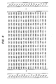
- FIG. 3 describes the matrix operation involved in computing a 16 x 16 cosine transform.
- the P elements represent the pel samples
- the numbers in the matrix are the cosine coefficients, (multiplied by 1000 merely to simplify the presentation) and the C elements represent the developed cosine transform coefficients.
- FIG. 4 presents one of a number of possible reorderings of the FIG. 3 matrix operation which highlights the symmetries present in the cosine coefficients matrix. This order produces segments or "blocks" in the matrix in which the constants on the left-bottom to top-right diagonals have the same absolute values.
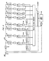
- FIG. 5 depicts an embodiment of the cosine transform circuit (20) of FIG. 1 which employs the symmetries apparent in FIG. 4.
- the FIG. 4 matrix can be segregated into two one coefficient segments (.707), a two coefficient segment (.923 and .382), a four coefficient segment (.980, .555, .195, and .831), and an eight coefficient segment (.995, .471, .773, .290, .098, .881, .634, and .956).
- the FIG. 5 circuit can be similarly segregated: e.g., multiplier 201 and its associated circuits, multipliers 202-203 and their associated circuitry, multipliers 204-207 and their associated circuits, and multipliers 208-215 and their associated circuits.
- multipliers 204-207 are responsive to input pel samples which are applied on line 200 in the order depicted in FIG. 4; to wit, p 0, P 5 , p 3 , P 6 , p 7 , p 2 , p 4 , P 1 , p 15 , P 10 , P 12 , p 9 , p 8 , p 13 , p 11 , and Pi4.
- Multipliers 204-207 develop output signals corresponding to the product of the signed input signals with the unsigned constants .980, .555, .195, and .831, respectively.
- Multipliers 204-207 (and the other multipliers in the FIG. 5 circuit - i.e., 201-203 and 208-215) are most simply implemented with small read-only memories, or combinations of read-only memories and adders as described, for example, in U. S. Patent application by S. Ganapathy, Serial No. 725,921, filed April 22, 1985.
- the output signals of multipliers 204-207 are applied to sign control circuits 304-307, respectively.
- Sign control circuits 304-307 account for the different signs that the multiplier coefficients must have (per the FIG. 4 matrix) under control of control signals applied by bus 300. More specifically, the circuit of FIG. 5 includes 15 sign control circuits (301-315) and, most simply, . bus 300 includes 15 leads; each connected to a different sign control circuit.
- the output of sign control circuit 304 is applied to adder 404 and the output of adder 404 is applied to register 504.
- the output of sign control circuit 305 and the output of register 504 are applied to adder 405 and the output of adder 405 is applied to register 505.
- the output of sign control circuit 306 and the output of register 505 are applied to adder 406 and the output of adder 406 is applied to register 506.
- the output of sign control circuit 307 and the output of register 506 are applied to adder 407 and the output of adder 407 is applied to register 507.
- Transform coefficient C 2 is developed by cycling through the sequence of multipliers .980, .555, .195, and .831. Offset by one, the transform coefficient C io is developed by cycling through the sequence of multipliers .555, .195, .831, and .980. Offset by one more, is transform coefficient C 14 , and lastly comes transform coefficient C 6 .
- the C 2 output is developed by multiplying P o in multiplier 204, temporarily storing the product in register 504, adding to that the product developed in multiplier 205 and storing it in register 505, adding to that the product developed in multiplier 206 and temporarily storing it in register 506 and, lastly, adding to that the product of multiplier 207.
- register 504 temporarily stores the partial product for transform coefficient C 2
- register 505 temporarily stores the partial product for coefficient C io
- register 506 stores the partial product for coefficient C 14
- register 507 stores the partial product for coefficient C 6 .
- the output of register 507 contains the coefficient C 2
- the output of register 504 contains the coefficient C lo
- the output of register 505 contains the coefficient C 14
- the output of register 506 contains the coefficient C 6 .
- These output coefficients are applied in the FIG. 5 circuit to parallel-to-serial converter register 600 which outputs on lead 601 a stream of the coefficients C o - C 3 in accordance with the order depicted in FIG. 4.
- the above-described four-coefficient segment is representative of other segments. They differ only in the number of multipliers and the number of stages in the cyclical pipeline accumulator, and in the constants by which the input signals are multiplied.
- All of the circuits making up the circuit of FIG. 5 are conventional digital elements.
- the representations of numbers can be in sign-magnitude form or any other signed representation. There is a slight advantage to the sign-magnitude form since elements 301-315 can simply perform on exclusive OR on the sign bit.
- Sign control ROM, 320 which develops the output signals on bus 300 is a small read-only memory. For the FIG. 5 circuit, it may simply be a 15x15 memory. Actually, additional symmetries can be employed to reduce the size of ROM 320, as well as the overall circuitry, as shown below.
- FIG. 6 shows a simple re-arrangement of the matrix multiplication in FIG. 4 that exploits this symmetry
- FIG. 7 presents an architecture that implements this: It replaces the 16 one-constant multipliers of FIG. 5 with 8 two-constant multipliers.
- Multiplexers 602-604 are arranged to permit calculation of either the even coefficients (with three independently operating segments) as specified by the upper portion of FIG. 6, or the odd coefficients (with one operating segment) as specified by the lower portion of FIG. 6.
- multiplexer switches 602-604 When used to calculate the odd coefficients, multiplexer switches 602-604 are connected to terminals II, as shown in FIG. 7; when used for the even, they are switched to terminals I. It may be noted that more symmetry exists in the top of the matrix and that this symmetry could be used to further reduce the number of multiplications required to calculate the even coefficients. However, as 8 multipliers are required anyway for the odd coefficients, there is little to be gained in doing so.
- Input adder module 605 provides for the appropriate delay and combining of the input signals, as specified by FIG.
- pels P o through P 1 are delayed in register 606, added to pels P 15 through P 14 respectively in adder 607, and passed to multipliers 701-708 through multiplexer switch 608. Concurrently, pels P 15 through P 14 are subtracted from the delayed pels P o through P 1 in element 609, and the developed difference signals are delayed in register 610 and applied through multiplexer switch 608 to multipliers 701-708.
- Multipliers 701-708 differ from multipliers 301-315 in that they are arranged to multiply by either one of two constants. Their implementation can be almost identical to that of multipliers 301-315. It may be noted that for sake of clarity that the FIG. 7 circuit does not show some of the obvious details.
- FIG. 8 illustrates another embodiment for adder module 605. It is more complex than the module depicted in FIG. 7, but, as will come to light below, the FIG. 8 module may be employed in the inverse discrete cosine transform as well.
- element 611 is a two-input and two-output arithmetic element. In response to inputs A and B, element 611 develops both A+B and A-B output signals. The A-B output is applied through multiplexer switch 612 to a 4-pel register 613, and the A+B output is applied to 2-pel register 614 and to 2-input multiplexer switch 615.
- the output of register 614 is applied to a second 2-pel register, 618, and to a first input of a 4-input multiplexer switch, 616.
- the output of register 618 is applied to a second input of switch 616, while the output of register 613 is applied to a third input of switch 616 and to the input of a second 4-pel register 617.
- the output of register 617 is applied to the fourth input of multiplexer switch 616 and to a second input of switch 615.
- switch 612 is connected to the "in" input (as shown in FIG. 8) and switch 615 is connected to the output of register 617.
- the output of register 617 (and hence at the output of switch 615) is P o - P 15 through P 1 - P 14 of the previous sequence of pel signals.
- pels P o through P 1 are stored in registers 617 and 613, switch 612 is connected to the A-B input, switch 615 is connected to the A+B output element of 611, and switch 616 is connected to the output of register 617.
- Pel signals P 15 thorough P 14 are then applied to the B input of element 611, yielding P o + P 15 at the A+B output of element 611 and, correspondingly, at the output of switch 615; while yielding P o - P 15 at the A-B output of 611 and into register 613 through switch 612.
- the sum signals P o + P 15 through P 1 + P 14 appear at the output while the difference signals P o - P 15 through P 1 - P 14 are stored within registers 613 and 617 for output at the next sequence, as referenced above.
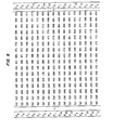
- FIG. 9 presents the inverse transform matrix equation.
- the matrix of coefficients employed in computing the inverse transform is the mathematical transpose of that of the forward transform and, accordingly, the transposes of the blocks segregated in FIG. 5 can also be segregated in FIG. 9.
- FIG. 9 presents the inverse transform matrix equation.
- the matrix of coefficients employed in computing the inverse transform is the mathematical transpose of that of the forward transform and, accordingly, the transposes of the blocks segregated in FIG. 5 can also be segregated in FIG. 9.
- three observations were made which led to the realization of the FIG.
- the input samples are transform coefficients C, in the order C o , C 8 , C 4 , C 12 , C 2 , C 10 , C 14 , C 6 , C 1 , Cn, C 7 , C 13 , C 15 , C 5 , Cg, and C 3
- the output is pel samples P, in the order P o , P s , P 3 , P 6 , P 7 , P 2 , P 4 , P 1 , P 15 , P 10 , P 12 , Pg, P 8 , P 13 , P n , and P 14 .
- FIG. 10 illustrates a rearranged version of the FIG. 9 matrix which highlights the horizontal as well as the vertical symmetries present in the . matrix.
- the output pel samples can be obtained by adding four components, as specified by the four columns. Elements [A, B], [C, D], [E, F, G, H], and [1, J, K, L, M, N, O, P] identified in the upper portion of FIG. 10 are computed as specified in the lower portion of FIG. 10.
- FIG. 11 is a transform generator that is capable of realizing both the forward discrete cosine transform and the inverse discrete cosine transform. Its operation in the forward transform mode has essentially been described earlier; so the following addresses only the inverse transform operation, except for the following comment.
- input signals on line 110 are applied to adder module 605 through multiplexer switch 111, and from there to line 200 through multiplexer switch 212.
- the output of the circuit is derived from parallel to serial converter 600 through multiplexer switch 113. Switches 111, 112, and 113 are shown in FIG. 11 in their inverse discrete cosine transform position.
- input signals (which are the cosine transform coefficients, C) are applied to bus 200 via multiplex switch 112 without going through adder module 605. It is assumed that the order of the applied cosine transform coefficients is as described above and depicted in FIG. 9. If a rearrangement in the order of the applied coefficients needs to be made, a memory may be provided to perform the reordering.
- the A and B components of FIG. 10 are computed with the aid of multipliers 701 and 702, respectively.
- the A component is stored in register 501 and the B component is stored in register 502.
- multipliers 703 and 704 are activated, and the cyclic pipeline accumulator segment of FIG. 11 which includes adders 403 an 404 and registers 503 and 504 develops the C and D components.
- the C component is stored in register 503 while the D component is stored in register 504.
- multipliers 705-708 are activated and the cyclic pipeline accumulator segment of FIG.
- registers 505-508 which contain those components, and the contents of registers 501-504 are transferred to parallel-to-serial converter 600.
- register 601 shifts its content through line 601 and switch 612 to adder module 605.
- multipliers 701-708 compute the I through P components in a manner identical to the computations performed in the forward transform.
- the contents of registers 505-508 are transferred to parallel-to-serial converter 600 and shifted out via line 601 to adder module 605.
- Adder module 605 receives the A through P components, seriatim, and its function is to add the various components in accordance with the specification embodied in the upper portion of FIG. 10. To develop P o , for example, it needs to compute the value of A+C+E+I. To develop P 7 , it needs to compute the value of A+C-E+M. This combining of the necessary components is accomplished in the adder module depicted in FIG. 8 by controlling switches 616 and 615 in accordance with the table below.
- the memories preceding these circuits must implement the sample orderings that are prescribed. This can be achieved with very simple combinatorial circuits or, simpler still, with very small read-only memories that control the writing and reading in the memories.
- FIGS. 2 and 3 The remaining circuitry in FIGS. 2 and 3 is completely conventional and is therefore left to the practitioner to select a design that best suits the designer.
- sequence 15, 10, 12, 9, 8, 13, 11, and 14 can be easily obtained by taking one's complement of the sequence 0, 5, 3, 6, 7, 2, 4, and 1; and that the latter sequence can easily be obtained by shifting right the binary representation of the sequence 1, 11, 7, 13, 15, 5, 9, and 3.
- the following presents a method by which the sequences can be obtained for 8, 16, and 32 point transforms.
- N is half the number of points in the transform
- p(x) be the xth pel subscript and c(x) be the xth coefficient subscript
- "x" represents the position of the subscript p(x) or c(x) in the list of subscripts.
- the resulting permutation sets that involve all values from 0 to N are valid (some will be degenerate).
- To find the corresponding c(x) the "ancestor" of each p(x) must be found by swapping values N apart such that the smaller ones end up on the left.
- the series p(x) 0 ⁇ x ⁇ N-1 will correspond to the first N terms of the "ancestor" 2N point transform.
- the final N subscripts are given by the following:
Landscapes
- Engineering & Computer Science (AREA)
- Physics & Mathematics (AREA)
- General Physics & Mathematics (AREA)
- Mathematical Physics (AREA)
- Theoretical Computer Science (AREA)
- Data Mining & Analysis (AREA)
- Pure & Applied Mathematics (AREA)
- Mathematical Analysis (AREA)
- Mathematical Optimization (AREA)
- Computational Mathematics (AREA)
- Signal Processing (AREA)
- Algebra (AREA)
- Discrete Mathematics (AREA)
- Databases & Information Systems (AREA)
- Software Systems (AREA)
- General Engineering & Computer Science (AREA)
- Multimedia (AREA)
- Complex Calculations (AREA)
- Compression Or Coding Systems Of Tv Signals (AREA)
Applications Claiming Priority (2)
| Application Number | Priority Date | Filing Date | Title |
|---|---|---|---|
| US06/876,076 US4829465A (en) | 1986-06-19 | 1986-06-19 | High speed cosine transform |
| US876076 | 1992-04-28 |
Publications (3)
| Publication Number | Publication Date |
|---|---|
| EP0250152A2 true EP0250152A2 (fr) | 1987-12-23 |
| EP0250152A3 EP0250152A3 (fr) | 1991-03-13 |
| EP0250152B1 EP0250152B1 (fr) | 1994-11-30 |
Family
ID=25366957
Family Applications (1)
| Application Number | Title | Priority Date | Filing Date |
|---|---|---|---|
| EP87305110A Expired - Lifetime EP0250152B1 (fr) | 1986-06-19 | 1987-06-10 | Circuit de transformation |
Country Status (7)
| Country | Link |
|---|---|
| US (1) | US4829465A (fr) |
| EP (1) | EP0250152B1 (fr) |
| JP (1) | JP2672302B2 (fr) |
| KR (1) | KR950012222B1 (fr) |
| CA (1) | CA1294053C (fr) |
| DE (1) | DE3750791T2 (fr) |
| ES (1) | ES2064315T3 (fr) |
Cited By (6)
| Publication number | Priority date | Publication date | Assignee | Title |
|---|---|---|---|---|
| DE4038240A1 (de) * | 1989-12-01 | 1991-06-06 | Ricoh Kk | Prozessor zum durchfuehren einer orthogonaltransformation |
| EP0467718A3 (en) * | 1990-07-20 | 1992-05-13 | Matsushita Electric Industrial Co., Ltd. | High efficiency coding apparatus and high efficiency decoding apparatus |
| GB2261969A (en) * | 1991-11-22 | 1993-06-02 | Intel Corp | Mutiplyless discrete cosine transform |
| EP0542261A3 (fr) * | 1991-11-12 | 1994-01-26 | Japan Broadcasting Corp | |
| EP0474246A3 (fr) * | 1990-09-06 | 1994-03-23 | Matsushita Electric Industrial Co Ltd | |
| US5359549A (en) * | 1989-12-01 | 1994-10-25 | Ricoh Company, Ltd. | Orthogonal transformation processor for compressing information |
Families Citing this family (64)
| Publication number | Priority date | Publication date | Assignee | Title |
|---|---|---|---|---|
| EP0576749B1 (fr) * | 1992-06-30 | 1999-06-02 | Discovision Associates | Système de données en pipeline |
| GB9405914D0 (en) * | 1994-03-24 | 1994-05-11 | Discovision Ass | Video decompression |
| FR2643477B1 (fr) * | 1989-02-23 | 1991-06-07 | France Etat | Procede de determination de transformee en cosinus discrete |
| JPH02237369A (ja) * | 1989-03-10 | 1990-09-19 | Casio Comput Co Ltd | 画像データ制御装置 |
| IT1235263B (it) * | 1989-06-02 | 1992-06-26 | Sgs Thomson Microelectronics | Metodo e dispositivo per il calcolo aritmetico di trasformate bidimensionali. |
| KR920008270B1 (ko) * | 1990-04-03 | 1992-09-26 | 정호선 | 신경회로망을 이용한 이산형 코사인 변환용 집적회로 |
| US5875266A (en) * | 1990-07-31 | 1999-02-23 | Fujitsu Limited | Image data processing a method and apparatus |
| US5933538A (en) * | 1990-07-31 | 1999-08-03 | Fujitsu Limited | Image data processing method and apparatus |
| EP0469855B1 (fr) | 1990-07-31 | 1999-12-01 | Fujitsu Limited | Méthode et appareil de traitement de données d'image |
| JPH04236664A (ja) * | 1991-01-18 | 1992-08-25 | Sony Corp | 演算回路 |
| JP2964172B2 (ja) * | 1991-03-08 | 1999-10-18 | 富士通株式会社 | Dctマトリクス演算回路 |
| JP2866754B2 (ja) * | 1991-03-27 | 1999-03-08 | 三菱電機株式会社 | 演算処理装置 |
| US5410500A (en) * | 1992-02-21 | 1995-04-25 | Sony Corporation | Discrete cosine transform apparatus and inverse discrete cosine transform apparatus |
| JP3323950B2 (ja) * | 1992-03-17 | 2002-09-09 | サン・マイクロシステムズ・インコーポレーテッド | デジタル画像処理システムでidctを実施する方法及びそのためのidctプロセッサ |
| US5224062A (en) * | 1992-03-17 | 1993-06-29 | Sun Microsystems, Inc. | Method and apparatus for fast implementation of inverse discrete cosine transform in a digital image processing system using optimized lookup tables |
| SG45281A1 (en) * | 1992-06-26 | 1998-01-16 | Discovision Ass | Method and arrangement for transformation of signals from a frequency to a time domain |
| US6067417A (en) * | 1992-06-30 | 2000-05-23 | Discovision Associates | Picture start token |
| US5768561A (en) * | 1992-06-30 | 1998-06-16 | Discovision Associates | Tokens-based adaptive video processing arrangement |
| US6079009A (en) * | 1992-06-30 | 2000-06-20 | Discovision Associates | Coding standard token in a system compromising a plurality of pipeline stages |
| US6330665B1 (en) | 1992-06-30 | 2001-12-11 | Discovision Associates | Video parser |
| US6047112A (en) * | 1992-06-30 | 2000-04-04 | Discovision Associates | Technique for initiating processing of a data stream of encoded video information |
| US5784631A (en) | 1992-06-30 | 1998-07-21 | Discovision Associates | Huffman decoder |
| US6112017A (en) * | 1992-06-30 | 2000-08-29 | Discovision Associates | Pipeline processing machine having a plurality of reconfigurable processing stages interconnected by a two-wire interface bus |
| US7095783B1 (en) | 1992-06-30 | 2006-08-22 | Discovision Associates | Multistandard video decoder and decompression system for processing encoded bit streams including start codes and methods relating thereto |
| US6435737B1 (en) | 1992-06-30 | 2002-08-20 | Discovision Associates | Data pipeline system and data encoding method |
| US5809270A (en) * | 1992-06-30 | 1998-09-15 | Discovision Associates | Inverse quantizer |
| US5394349A (en) * | 1992-07-10 | 1995-02-28 | Xing Technology Corporation | Fast inverse discrete transform using subwords for decompression of information |
| KR940004467A (ko) * | 1992-08-26 | 1994-03-15 | 오오가 노리오 | 이산코사인 변환장치 및 그 역변환장치 |
| JPH06103301A (ja) * | 1992-09-17 | 1994-04-15 | Sony Corp | 8x8離散コサイン変換回路および8x8離散コサイン逆変換回路 |
| US5523847A (en) * | 1992-10-09 | 1996-06-04 | International Business Machines Corporation | Digital image processor for color image compression |
| JPH06149862A (ja) * | 1992-11-13 | 1994-05-31 | Sony Corp | 行列データ乗算方法及び行列データ乗算装置 |
| JP2951135B2 (ja) * | 1992-11-30 | 1999-09-20 | 三星電子株式会社 | パルスレーダのクラッタ除去器 |
| KR950000386B1 (ko) * | 1992-12-30 | 1995-01-16 | 재단법인 한국전자통신연구소 | 이산여현 변환회로 |
| US5805914A (en) * | 1993-06-24 | 1998-09-08 | Discovision Associates | Data pipeline system and data encoding method |
| US5699544A (en) * | 1993-06-24 | 1997-12-16 | Discovision Associates | Method and apparatus for using a fixed width word for addressing variable width data |
| US5768629A (en) * | 1993-06-24 | 1998-06-16 | Discovision Associates | Token-based adaptive video processing arrangement |
| US5861894A (en) * | 1993-06-24 | 1999-01-19 | Discovision Associates | Buffer manager |
| JP2997613B2 (ja) * | 1993-10-26 | 2000-01-11 | 株式会社東芝 | 離散コサイン変換装置 |
| US5638068A (en) * | 1993-11-24 | 1997-06-10 | Intel Corporation | Processing images using two-dimensional forward transforms |
| US5729484A (en) * | 1994-02-28 | 1998-03-17 | Intel Corporation | Processes, apparatuses, and systems of encoding and decoding signals using transforms |
| CA2145379C (fr) * | 1994-03-24 | 1999-06-08 | William P. Robbins | Methode et dispositif d'adressage memoire |
| CA2145361C (fr) * | 1994-03-24 | 1999-09-07 | Martin William Sotheran | Gestionnaire de tampons |
| CA2145365C (fr) * | 1994-03-24 | 1999-04-27 | Anthony M. Jones | Methode d'acces a des batteries de memoires vives dynamiques |
| US5428567A (en) * | 1994-05-09 | 1995-06-27 | International Business Machines Corporation | Memory structure to minimize rounding/trunction errors for n-dimensional image transformation |
| GB9417138D0 (en) | 1994-08-23 | 1994-10-12 | Discovision Ass | Data rate conversion |
| US5636152A (en) * | 1995-04-28 | 1997-06-03 | United Microelectronics Corporation | Two-dimensional inverse discrete cosine transform processor |
| US5504455A (en) * | 1995-05-16 | 1996-04-02 | Her Majesty The Queen In Right Of Canada, As Represented By The Minister Of National Defence Of Her Majesty's Canadian Government | Efficient digital quadrature demodulator |
| US5701263A (en) * | 1995-08-28 | 1997-12-23 | Hyundai Electronics America | Inverse discrete cosine transform processor for VLSI implementation |
| US5729691A (en) * | 1995-09-29 | 1998-03-17 | Intel Corporation | Two-stage transform for video signals |
| US5854757A (en) * | 1996-05-07 | 1998-12-29 | Lsi Logic Corporation | Super-compact hardware architecture for IDCT computation |
| US6507898B1 (en) * | 1997-04-30 | 2003-01-14 | Canon Kabushiki Kaisha | Reconfigurable data cache controller |
| US6134270A (en) * | 1997-06-13 | 2000-10-17 | Sun Microsystems, Inc. | Scaled forward and inverse discrete cosine transform and video compression/decompression systems employing the same |
| AUPP217798A0 (en) | 1998-03-06 | 1998-03-26 | Liguori, Vincenzo | A simple discrete cosine transform implementation |
| US6421696B1 (en) | 1999-08-17 | 2002-07-16 | Advanced Micro Devices, Inc. | System and method for high speed execution of Fast Fourier Transforms utilizing SIMD instructions on a general purpose processor |
| US6754687B1 (en) | 1999-11-12 | 2004-06-22 | Pts Corporation | Methods and apparatus for efficient cosine transform implementations |
| WO2001035267A1 (fr) * | 1999-11-12 | 2001-05-17 | Bops, Incorporated | Procede et appareil permettant de mettre en oeuvre une transformee de cosinus efficace |
| US7292730B1 (en) * | 1999-12-09 | 2007-11-06 | Intel Corporation | Two-dimensional inverse discrete cosine transforming |
| US7054897B2 (en) * | 2001-10-03 | 2006-05-30 | Dsp Group, Ltd. | Transposable register file |
| US7792891B2 (en) * | 2002-12-11 | 2010-09-07 | Nvidia Corporation | Forward discrete cosine transform engine |
| US8423597B1 (en) | 2003-08-29 | 2013-04-16 | Nvidia Corporation | Method and system for adaptive matrix trimming in an inverse discrete cosine transform (IDCT) operation |
| KR100709731B1 (ko) * | 2005-07-14 | 2007-04-19 | 주식회사 케이엔텍 | 샤워기용 절수장치 |
| KR101088375B1 (ko) * | 2005-07-21 | 2011-12-01 | 삼성전자주식회사 | 가변 블록 변환 장치 및 방법 및 이를 이용한 영상부호화/복호화 장치 및 방법 |
| WO2009095087A2 (fr) * | 2008-01-31 | 2009-08-06 | Qualcomm Incorporated | Dispositif pour calcul de dft |
| US9798698B2 (en) | 2012-08-13 | 2017-10-24 | Nvidia Corporation | System and method for multi-color dilu preconditioner |
Family Cites Families (9)
| Publication number | Priority date | Publication date | Assignee | Title |
|---|---|---|---|---|
| US2662161A (en) * | 1949-04-29 | 1953-12-08 | Asea Ab | Electric eddy current furnace |
| US3662161A (en) * | 1969-11-03 | 1972-05-09 | Bell Telephone Labor Inc | Global highly parallel fast fourier transform processor |
| FR2262350B1 (fr) * | 1974-02-25 | 1976-12-03 | France Etat | |
| US4152772A (en) * | 1974-08-29 | 1979-05-01 | The United States Of America As Represented By The Secretary Of The Navy | Apparatus for performing a discrete cosine transform of an input signal |
| FR2326743A1 (fr) * | 1975-10-02 | 1977-04-29 | Thomson Csf | Calculateur de transformee de fourier discrete |
| US4196448A (en) * | 1978-05-15 | 1980-04-01 | The United States Of America As Represented By The Secretary Of The Navy | TV bandwidth reduction system using a hybrid discrete cosine DPCM |
| US4385363A (en) * | 1978-12-15 | 1983-05-24 | Compression Labs, Inc. | Discrete cosine transformer |
| JPS57146345A (en) * | 1981-03-04 | 1982-09-09 | Toshiba Corp | 3n-th degree orthogonal transformation and inverse transformation system |
| US4449194A (en) * | 1981-09-25 | 1984-05-15 | Motorola Inc. | Multiple point, discrete cosine processor |
-
1986
- 1986-06-19 US US06/876,076 patent/US4829465A/en not_active Expired - Lifetime
-
1987
- 1987-06-10 DE DE3750791T patent/DE3750791T2/de not_active Expired - Fee Related
- 1987-06-10 EP EP87305110A patent/EP0250152B1/fr not_active Expired - Lifetime
- 1987-06-10 ES ES87305110T patent/ES2064315T3/es not_active Expired - Lifetime
- 1987-06-16 CA CA000539796A patent/CA1294053C/fr not_active Expired - Lifetime
- 1987-06-17 KR KR1019870006111A patent/KR950012222B1/ko not_active Expired - Fee Related
- 1987-06-19 JP JP62151545A patent/JP2672302B2/ja not_active Expired - Fee Related
Cited By (12)
| Publication number | Priority date | Publication date | Assignee | Title |
|---|---|---|---|---|
| DE4038240A1 (de) * | 1989-12-01 | 1991-06-06 | Ricoh Kk | Prozessor zum durchfuehren einer orthogonaltransformation |
| US5268853A (en) * | 1989-12-01 | 1993-12-07 | Ricoh Company, Ltd. | Orthogonal transformation processor for compressing information |
| US5331585A (en) * | 1989-12-01 | 1994-07-19 | Ricoh Company, Ltd. | Orthogonal transformation processor for compressing information |
| US5359549A (en) * | 1989-12-01 | 1994-10-25 | Ricoh Company, Ltd. | Orthogonal transformation processor for compressing information |
| EP0467718A3 (en) * | 1990-07-20 | 1992-05-13 | Matsushita Electric Industrial Co., Ltd. | High efficiency coding apparatus and high efficiency decoding apparatus |
| US5196930A (en) * | 1990-07-20 | 1993-03-23 | Matsushita Electric Industrial Co., Ltd. | High efficienccy coding and decoding apparatus for lowering transmission or recording rate of transmitted or recorded video signal without reducing picture quality |
| EP0474246A3 (fr) * | 1990-09-06 | 1994-03-23 | Matsushita Electric Industrial Co Ltd | |
| EP0542261A3 (fr) * | 1991-11-12 | 1994-01-26 | Japan Broadcasting Corp | |
| US5534927A (en) * | 1991-11-12 | 1996-07-09 | Nippon Hoso Kyokai | Method of performing high efficiency coding of image signal and system therefor |
| GB2261969A (en) * | 1991-11-22 | 1993-06-02 | Intel Corp | Mutiplyless discrete cosine transform |
| US5285402A (en) * | 1991-11-22 | 1994-02-08 | Intel Corporation | Multiplyless discrete cosine transform |
| GB2261969B (en) * | 1991-11-22 | 1995-11-22 | Intel Corp | Multiplyless discrete cosine transform |
Also Published As
| Publication number | Publication date |
|---|---|
| JP2672302B2 (ja) | 1997-11-05 |
| EP0250152A3 (fr) | 1991-03-13 |
| ES2064315T3 (es) | 1995-02-01 |
| KR950012222B1 (ko) | 1995-10-16 |
| DE3750791D1 (de) | 1995-01-12 |
| EP0250152B1 (fr) | 1994-11-30 |
| CA1294053C (fr) | 1992-01-07 |
| JPS6332660A (ja) | 1988-02-12 |
| KR880000879A (ko) | 1988-03-30 |
| US4829465A (en) | 1989-05-09 |
| DE3750791T2 (de) | 1995-05-18 |
Similar Documents
| Publication | Publication Date | Title |
|---|---|---|
| EP0250152B1 (fr) | Circuit de transformation | |
| US5467131A (en) | Method and apparatus for fast digital signal decoding | |
| KR960003648B1 (ko) | 화상데이타 처리방법 및 장치 | |
| US5299025A (en) | Method of coding two-dimensional data by fast cosine transform and method of decoding compressed data by inverse fast cosine transform | |
| JP5507077B2 (ja) | バタフライプロセッサを使用して離散コサイン変換をエンコードしそして計算するための装置及び方法 | |
| US5659362A (en) | VLSI circuit structure for implementing JPEG image compression standard | |
| US5196930A (en) | High efficienccy coding and decoding apparatus for lowering transmission or recording rate of transmitted or recorded video signal without reducing picture quality | |
| US6317767B2 (en) | Methods and systems for performing short integer chen IDCT algorithm with fused multiply/add | |
| US20050038843A1 (en) | Apparatus and method for decoding and computing a discrete cosine transform using a butterfly processor | |
| US7076105B2 (en) | Circuit and method for performing a two-dimensional transform during the processing of an image | |
| EP1544797A2 (fr) | Coprocesseur de calcul d'une transformation pour la compression vidéo à haute performance et à faible consommation d'énergie | |
| Uma | FPGA implementation of 2-D DCT for JPEG image compression | |
| Lee et al. | Design of high-performance transform and quantization circuit for unified video CODEC | |
| GB2139046A (en) | Video signal transmission | |
| KR960014196B1 (ko) | 이차원 역 이산 코사인 변환(idct) 프로세서 | |
| KR0180773B1 (ko) | 여현변환/역여현변환/양자화/역양자화 연산을 수용하는 벡터 처리 장치 | |
| KR19980073563A (ko) | 이산여현 변환 및 역변환 프로세서 | |
| KR19980021019A (ko) | 2차원 아이디씨티 장치 | |
| Suh et al. | A design of DPCM hybrid coding loop using single 1-d DCT in MPEG-2 video encoder | |
| Fernández et al. | RNS Implementation of Two Dimensional Discrete Cosine Transform over FPL Devices | |
| Yang | A distributed arithmetic based CORDIC algorithm and its use in the FPGA implementation of the 2-D IDCT | |
| Vanitha et al. | Design and Implementation of Image Compression Encoder using Orthogonal Approximation DCT | |
| JPH0487466A (ja) | 画像データ符号化・復元装置 | |
| JPH0468969A (ja) | 量子化・逆量子化方法及び装置 |
Legal Events
| Date | Code | Title | Description |
|---|---|---|---|
| PUAI | Public reference made under article 153(3) epc to a published international application that has entered the european phase |
Free format text: ORIGINAL CODE: 0009012 |
|
| AK | Designated contracting states |
Kind code of ref document: A2 Designated state(s): DE ES GB NL |
|
| PUAL | Search report despatched |
Free format text: ORIGINAL CODE: 0009013 |
|
| AK | Designated contracting states |
Kind code of ref document: A3 Designated state(s): DE ES GB NL |
|
| 17P | Request for examination filed |
Effective date: 19910905 |
|
| 17Q | First examination report despatched |
Effective date: 19921222 |
|
| RAP3 | Party data changed (applicant data changed or rights of an application transferred) |
Owner name: AT&T CORP. |
|
| GRAA | (expected) grant |
Free format text: ORIGINAL CODE: 0009210 |
|
| AK | Designated contracting states |
Kind code of ref document: B1 Designated state(s): DE ES GB NL |
|
| REF | Corresponds to: |
Ref document number: 3750791 Country of ref document: DE Date of ref document: 19950112 |
|
| REG | Reference to a national code |
Ref country code: ES Ref legal event code: FG2A Ref document number: 2064315 Country of ref document: ES Kind code of ref document: T3 |
|
| PLBE | No opposition filed within time limit |
Free format text: ORIGINAL CODE: 0009261 |
|
| STAA | Information on the status of an ep patent application or granted ep patent |
Free format text: STATUS: NO OPPOSITION FILED WITHIN TIME LIMIT |
|
| 26N | No opposition filed | ||
| REG | Reference to a national code |
Ref country code: GB Ref legal event code: IF02 |
|
| PGFP | Annual fee paid to national office [announced via postgrant information from national office to epo] |
Ref country code: GB Payment date: 20020527 Year of fee payment: 16 |
|
| PGFP | Annual fee paid to national office [announced via postgrant information from national office to epo] |
Ref country code: NL Payment date: 20020531 Year of fee payment: 16 |
|
| PGFP | Annual fee paid to national office [announced via postgrant information from national office to epo] |
Ref country code: ES Payment date: 20020604 Year of fee payment: 16 |
|
| PGFP | Annual fee paid to national office [announced via postgrant information from national office to epo] |
Ref country code: DE Payment date: 20020628 Year of fee payment: 16 |
|
| PG25 | Lapsed in a contracting state [announced via postgrant information from national office to epo] |
Ref country code: GB Free format text: LAPSE BECAUSE OF NON-PAYMENT OF DUE FEES Effective date: 20030610 |
|
| PG25 | Lapsed in a contracting state [announced via postgrant information from national office to epo] |
Ref country code: ES Free format text: LAPSE BECAUSE OF NON-PAYMENT OF DUE FEES Effective date: 20030611 |
|
| PG25 | Lapsed in a contracting state [announced via postgrant information from national office to epo] |
Ref country code: NL Free format text: LAPSE BECAUSE OF NON-PAYMENT OF DUE FEES Effective date: 20040101 Ref country code: DE Free format text: LAPSE BECAUSE OF NON-PAYMENT OF DUE FEES Effective date: 20040101 |
|
| GBPC | Gb: european patent ceased through non-payment of renewal fee |
Effective date: 20030610 |
|
| NLV4 | Nl: lapsed or anulled due to non-payment of the annual fee |
Effective date: 20040101 |
|
| REG | Reference to a national code |
Ref country code: ES Ref legal event code: FD2A Effective date: 20030611 |