EP0251277A2 - Système d'enregistrement et de reproduction pour milieu d'enregistrement magnétique - Google Patents
Système d'enregistrement et de reproduction pour milieu d'enregistrement magnétique Download PDFInfo
- Publication number
- EP0251277A2 EP0251277A2 EP87109331A EP87109331A EP0251277A2 EP 0251277 A2 EP0251277 A2 EP 0251277A2 EP 87109331 A EP87109331 A EP 87109331A EP 87109331 A EP87109331 A EP 87109331A EP 0251277 A2 EP0251277 A2 EP 0251277A2
- Authority
- EP
- European Patent Office
- Prior art keywords
- data
- pll circuit
- read
- recording medium
- pulses
- Prior art date
- Legal status (The legal status is an assumption and is not a legal conclusion. Google has not performed a legal analysis and makes no representation as to the accuracy of the status listed.)
- Granted
Links
Images


Classifications
-
- G—PHYSICS
- G06—COMPUTING OR CALCULATING; COUNTING
- G06F—ELECTRIC DIGITAL DATA PROCESSING
- G06F1/00—Details not covered by groups G06F3/00 - G06F13/00 and G06F21/00
-
- G—PHYSICS
- G11—INFORMATION STORAGE
- G11B—INFORMATION STORAGE BASED ON RELATIVE MOVEMENT BETWEEN RECORD CARRIER AND TRANSDUCER
- G11B27/00—Editing; Indexing; Addressing; Timing or synchronising; Monitoring; Measuring tape travel
- G11B27/10—Indexing; Addressing; Timing or synchronising; Measuring tape travel
- G11B27/19—Indexing; Addressing; Timing or synchronising; Measuring tape travel by using information detectable on the record carrier
- G11B27/28—Indexing; Addressing; Timing or synchronising; Measuring tape travel by using information detectable on the record carrier by using information signals recorded by the same method as the main recording
- G11B27/30—Indexing; Addressing; Timing or synchronising; Measuring tape travel by using information detectable on the record carrier by using information signals recorded by the same method as the main recording on the same track as the main recording
- G11B27/3027—Indexing; Addressing; Timing or synchronising; Measuring tape travel by using information detectable on the record carrier by using information signals recorded by the same method as the main recording on the same track as the main recording used signal is digitally coded
-
- G—PHYSICS
- G11—INFORMATION STORAGE
- G11B—INFORMATION STORAGE BASED ON RELATIVE MOVEMENT BETWEEN RECORD CARRIER AND TRANSDUCER
- G11B19/00—Driving, starting, stopping record carriers not specifically of filamentary or web form, or of supports therefor; Control thereof; Control of operating function ; Driving both disc and head
- G11B19/02—Control of operating function, e.g. switching from recording to reproducing
- G11B19/04—Arrangements for preventing, inhibiting, or warning against double recording on the same blank or against other recording or reproducing malfunctions
-
- G—PHYSICS
- G11—INFORMATION STORAGE
- G11B—INFORMATION STORAGE BASED ON RELATIVE MOVEMENT BETWEEN RECORD CARRIER AND TRANSDUCER
- G11B20/00—Signal processing not specific to the method of recording or reproducing; Circuits therefor
- G11B20/10—Digital recording or reproducing
- G11B20/12—Formatting, e.g. arrangement of data block or words on the record carriers
- G11B20/1217—Formatting, e.g. arrangement of data block or words on the record carriers on discs
- G11B20/1252—Formatting, e.g. arrangement of data block or words on the record carriers on discs for discontinuous data, e.g. digital information signals or computer program data
-
- G—PHYSICS
- G11—INFORMATION STORAGE
- G11B—INFORMATION STORAGE BASED ON RELATIVE MOVEMENT BETWEEN RECORD CARRIER AND TRANSDUCER
- G11B20/00—Signal processing not specific to the method of recording or reproducing; Circuits therefor
- G11B20/10—Digital recording or reproducing
- G11B20/14—Digital recording or reproducing using self-clocking codes
- G11B20/1403—Digital recording or reproducing using self-clocking codes characterised by the use of two levels
-
- G—PHYSICS
- G11—INFORMATION STORAGE
- G11B—INFORMATION STORAGE BASED ON RELATIVE MOVEMENT BETWEEN RECORD CARRIER AND TRANSDUCER
- G11B27/00—Editing; Indexing; Addressing; Timing or synchronising; Monitoring; Measuring tape travel
- G11B27/10—Indexing; Addressing; Timing or synchronising; Measuring tape travel
-
- G—PHYSICS
- G11—INFORMATION STORAGE
- G11B—INFORMATION STORAGE BASED ON RELATIVE MOVEMENT BETWEEN RECORD CARRIER AND TRANSDUCER
- G11B2220/00—Record carriers by type
- G11B2220/20—Disc-shaped record carriers
Definitions
- the present invention relates to a recording/reproducing system for a magnetic recording medium.
- a preceding-erase type magnetic head In the field of floppy disk apparatuses, a preceding-erase type magnetic head has recently been devised, which is suitable for use with a high-density magnetic recording medium (disk).
- an erase head In the preceding-erase type magnetic head, an erase head is located in front of a read/write head in the rotational direction of the medium. Before new data are recorded in the medium by the read/write head, previously recorded data are first erased by the erase head.
- the erase head should preferably be turned on at a predetermined time before the recording of data on the medium by the read/write head begins, and turned off at a predetermined time before the recording of data end.
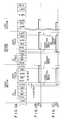
- a track of a magnetic recording medium has a format shown in Fig. lA, i.e. in which one sector comprises an ID field and a data field.
- the ID field comprises a synchronization area SYNC, address mark area AM, identification area ID, and cyclic redundancy check area CRC. Information representative of the starting position and address of a sector are recorded in the ID field.
- the data field records data, and comprises synchronization area SYNC, address mark area AM, data area DATA, and cyclic redundancy check area CRC.
- Synchronization areas SYNC store synchronization data for a PLL circuit
- address mark AM areas store address mark data indicative of the starting position of the ID field or the data field
- ID area ID stores data such as the cylinder number, the side number, the sector number, and the length of the data field
- data areas DATA store data read out or written in by a user
- cyclic redundancy check areas CRC store data for checking whether or not the data read out from the ID field or the data field contains an error.
- Gaps l, 2, 3, and 4 are areas for absorbing a fluctuation of rotation and an error in a mechanical alignment.
- Fig. lD shows a configuration of a preceding-erase type magnetic head.
- the magnetic head has an erase head, a read/write head and a separator.
- the separator magnetically separates the erase head from the read/write head.
- the erase head is located in front of the read/write head with respect to the rotational direction Z of a recording medium.
- Data read out from the recording medium by the magnetic head are fed to a data separator which includes a PLL circuit and an external synchronization detecting circuit.
- the external synchronization detector detects the synchronization data in the read data, and upon detection of the synchronization data, the PLL circuit begins oscillating in synchronism with the read data and outputs data pulses and clock pulses.
- an internal synchronization detector detects the synchronization data on the bases of the data pulses and the clock pulses, and a floppy disk controller checks whether or not the following data are address mark data.
- the floppy disk controller When the address mark data are detected, the floppy disk controller reads out the data stored in the ID area ID or in data area DATA, on the basis of the data pulses and clock pulses. When data other than the address mark data are detected, the floppy disk controller stops operating for a predetermined time period, and then repeats the above-mentioned operation.
- Figs. lB and lC show the positions where the erase head and read/write head of the preceding-erase type magnetic head are turned on and off during data are written in the medium. As is shown in Figs. lA to lC, over-written areas are formed in Gap 2, where data are not erased by the erase head and new data are overlapped by recorded on the previously recorded data.
- the floppy disk controller performs the above operation, it cannot read out the data of the data field which follows the boundary.
- An object of the present invention is to provide a a high reliability recording/reproducing system which uses a preceding-erase type magnetic head.
- a recording/reproducing system which comprises a magnetic head of preceding-erase type, in contact with a flexible magnetic recording medium, for recording data on said magnetic recording medium and reading out data stored in said recording medium, said magnetic head having a read/write head for writing data on, and reading data from, said magnetic recording medium, and an erase head arranged in front of said read/write head for erasing data recorded on said magnetic recording medium; write means for turning said read/write head and said erase head on substantially simultaneously and for supplying a specified signal to said read/write head, thereby to erasing data recorded on said magnetic recording medium, and to write data on said magnetic recording medium; digital signal-outputting means for outputting a digital signal corresponding to the data read out by said read/write head from said magnetic recording medium; PLL (Phase Locked Loop) circuit means for receiving the digital signal, and for oscillating in synchronism with the digital signal, thereby to output data pulses and clock pulses; readout means for receiving the data pulses and the
- the data pulses (DP) and the clock pulses (CP) are prevented from being output from the PLL circuit means (27), during the time period that the digital signal (RD) reproduced from the overwritten area (GAP2) of the magnetic recording medium (l3) is supplied to the PLL circuit means (27).
- the reading means (29) detects the data recorded in the overwritten area (GAP2) as the synchronization data, and that consequently the address mark detect error will occur.
- the recording/reproducing system with high reliability can be realized.
- Magnetic head ll of floppy disk apparatus (FDP) l0 has an erase head and a read/write head same as Fig. lD.
- FDC 29 receives write data WD from a host computer (not shown), and supplies write data WD to write circuit 53.
- FDC 29 also supplies gate signal GS to write circuit 53 and selector 5l.
- Gate signal GS functions as a write gate signal, an erase gate signal and a select signal.
- the write gate signal and the erase gate signal are supplied to write circuit 53.
- the select signal is supplied to selector 5l.
- Selector 5l supplies write signal to the read/write head when the select signal is ON level.
- Selector 5l supplies output signal of the read/write head to prestage circuit l5 when the select signal is OFF level.
- Prestage circuit l5 is made up of an amplifier circuit, a time domain filter, and the like.
- Prestage circuit l5 amplifies the input signal, converts the output of magnetic head ll into digital data, and outputs the data.
- the output data of prestage circuit l5 is supplied to external synchronization detect circuit 2l of data separator circuit 20 as read data RD.
- External synchronization detect circuit 2l detects the synchronization area of recording medium l3 on the basis of read data RD.
- external synchronization detect circuit 2l detects the synchronization data (fixed zero pattern data) recorded in the synchronization area on the basis of read data RD.
- External synchronization detect circuit 2l outputs an H-level pulse when it detects the synchronization data.
- the output signal S of external synchronization detect circuit 2l is supplied to the clock terminal CK of first D-type flip-flop (first D FF) 23.
- the D terminal of first D FF 23 is connected to an H level.
- Read gate signal RG to be described later is supplied to the low active CLR terminal of first D FF 23.
- First D FF 23 latches the H level signal at the leading edge of the output signal S of external synchronization detect circuit 2l.
- the Q output Ql of first D FF 23 is supplied to the the other input terminal of AND gate 25.
- Output signal PG of AND gate 25 is supplied to the control terminal C of phase locked loop (PLL) circuit 27.
- the read data RD is also supplied to the input terminal I of PLL circuit 27.
- PLL circuit 27 is provided with a voltage controlled oscillator in it, and operates so that the phase of the output pulses is equal to that of the input pulses.
- PLL circuit 27 oscillates in synchronism with the read data RD, and separates the read data RD into data pulses DP and clock pulses CP (read operation).
- Data pulses DP are a pulse signal representing the data as written into the data areas on the tracks of the recording medium l3.
- Clock pulses CP are a pulse signal representing the timing for reading out data.
- PLL circuit 27 when the signal supplied to control terminal C is low in level, oscillates in synchronism with the clock signal (at the write center frequency), which is contained in the PLL circuit per se.
- Data pulses DP and clock pulses CP, which are output from PLL circuit 27, are supplied to floppy disk controller (FDC) 29.
- FDC 29 is connected to a host computer (not shown), and the like.
- FDC 29 receives a read command from the host computer, and controls read gate signal RG, thereby to control read operation.
- the data pulses DP and the clock pulses CP are also supplied to internal synchronization detect circuit 3l.
- internal synchronization detect circuit 3l Upon detect of the synchronization data, internal synchronization detect circuit 3l outputs H level signal SYNC on the basis of the data pulses DP and the clock pulses CP, which come from PLL circuit 27.
- the output signal from internal synchronization detect circuit 3l is supplied to FDC 29.
- FDC 29 when the signal SYNC is high, executes the read/write operation of data.
- the data pulse DP and the clock pulse DP which come from PLL circuit 27, are also supplied to address mark detect circuit 33.
- This circuit 33 detects address mark data (predetermined pattern data) as stored in the address mark areas in the tracks on recording medium l3, on the basis of the data pulses DP and the clock pulses CP. It then outputs H-level signal SAD.
- Output signal PG of AND gate 25 is supplied to the low active clear terminal CLR of address mark detect circuit 33.
- the signal SAD is supplied to clock terminal CK of second D FF 35.
- Read gate signal RG (to be described later) is supplied to the D terminal of second D FF 35.
- the signal PG of AND gate 25 is supplied to the low active clear terminal CLR of second D FF 35.
- second D FF 35 At the leading edge of signal SAD, second D FF 35 outputs an H-level signal.
- the Q output Q2 of second D FF 35 is supplied to the input terminal of AND gate 37.
- Read gate signal RG is supplied to the low active, other input terminal of AND gate 37.
- the output signal of AND gate 37 is supplied to the clock terminal CK of monostable multi-vibrator (one-shot) (MMV) 39.
- MMV 39 outputs a pulse signal to the other input terminal of AND gate 25.
- the pulse signal is kept at low level during time period Tg.
- Each track of magnetic recording medium l3 of this embodiment also has a format shown in Fig. lA. And, when the data is recorded, the on/off of the erase head, and the on/off of the read/write head are timed as shown in Figs. lB and lC.
- the host computer supplies a write command to FDC 29.
- FDC 29 causes the gate signal GS to rise to H level.
- Gate signal GS functions as write gate signal, erase gate signal and select signal.
- Write circuit 53 receivers the write gate signal and the erase gate signal. When the write gate signal and the erase gate signal is H level, write circuit 53 generates a write signal and erase signal on the bases of write data WD supplied from the host computer via FDC 29 to write circuit 53.
- Write circuit 53 supplies the write signal to selector 5l, and the erase signal to the erase head. When the select signal rises to H level, selector 5l supplies the write signal, which has been supplied from write circuit 53, to the read/write head.
- the data previously recorded on medium l3 is erased by the erase head, and new data is recorded on medium l3 by the read/write head.
- FDC 29 causes gate signal GS fall to L level.
- gate signal GS falls to L level
- write circuit 53 stops generating the erase signal and the write signal.
- read/write head reads the data recorded on medium l3, and outputs a signal corresponding to this data.
- selector 5l supplies the output signal of the read/write head to prestage circuit l5.
- Prestage circuit l5 outputs read data RD.
- external synchronization detect circuit 2l When external synchronization detect circuit 2l detects the synchronization data (predetermined zero pattern data) from read data RD, it outputs an H-level pulse to clock terminal CK of first D FF 30. At the leading edge of the pulse, first D FF 30 latches the H-level signal, and outputs H-level signal Ql to AND gate 25.
- output M of MMV 39 is at high level, as shown in Fig. 3F.
- AND gate 25 outputs H-level signal PG to PLL circuit 27, as shown in Fig. 3C.
- PLL circuit 27 starts the synchronizing operation for read data RD.
- PLL circuit 27 oscillates in synchronism with read data RD, and separates data pulses DP and clock pulses CP from read pulse RD, and outputs the pulses.
- internal synchronization detect circuit 3l detects the synchronization data.
- circuit 3l outputs H-level signal SYNC.
- FDC 29 starts the data read operation.
- Data pulses DP and clock pulses CP from PLL circuit 27 are supplied to address mark detect circuit 33.
- address mark detect circuit 33 detects the address mark data recorded in address mark area AM in the ID field. It then outputs pulse signal SAD, as shown in Fig. 3D.
- pulse signal SAD As shown in Fig. 3D.
- second D FF 35 latches read gate signal RG.
- read gate signal RG is at high level, as shown in Fig. 3B, second D FF 32 outputs H-level signal Q2, as shown in Fig. 3E.
- AND gate 37 keeps the outputting of the L-level signal, because read gate signal RG is high.
- MMV 39 keeps the outputting of H-level signal M, because no trigger is input to MMV 39.
- AND gate 25 also keeps the outputting of H-level signal PG.
- FDC 29 reads out the data recorded in the ID field.
- FDC 29 After completing the read operation for the ID field, FDC 29 resets read gate signal RG to the low level (Fig. 3B).
- AND gate 37 Upon receipt of L-level read gate signal RG, AND gate 37 outputs an H-level signal to MMV 39. With the trigger of the leading edge of the output signal of AND gate 37, MMV 39 outputs negative pulse M.
- the pulse M keeps its L-level during fixed period of time Tg, as shown in Fig. 3F.
- the pulse width Tg is substantially equal to the time required for magnetic head ll to read areas GAP 2 in the tracks. In other words, the pulse width Tg is substantially equal to the required for read data RD reproduced from the data overwritten area in the tracks to be supplied to PLL circuit 27.
- PLL circuit 27 Upon receipt of negative pulse M, AND gate 25 renders control signal PG low in level, as shown in Fig. 3C.
- PLL circuit 27 Upon receipt of L-level control signal PG, PLL circuit 27 stops the synchronizing operation for read data RD, and stops the operation for separating data pulses DP and clock pulses CP from read data RD. PLL circuit 27 synchronizes with the clock in the PLL circuit 27.
- first D FF 23 When supplied with L-level read gate signal RG, first D FF 23 is cleared. When supplied with L-level signal PG, address mark detect circuit 33 and second FF 35 are also cleared.
- FDC 29 again renders read gate signal RG high. Afterwards, when external synchronization detect circuit 2l detects the synchronization data, the same operation as the read operation for ID field is started. PLL circuit 27 then performs the synchronizing operation for read data RD. FDC 29 performs the data readout.
- FDC 29 When the data field has been read, FDC 29 renders read gate signal RG low.
- PLL circuit 27 Upon receipt of negative pulse M, PLL circuit 27 stops the synchronizing operation for read data RD during fixed time period Tg. This stoppage prevents PLL circuit 27 from synchronizing with the read data RD at varying frequency that is reproduced from the DC erased area of the tracks.
- PLL circuit 27 does not perform the synchronizing operation for read data RD.
- PLL circuit 27 does not perform the synchronizing operation for read data RD.
- Even if the same data as the synchronization data is recorded in the overwritten area (GAP2) there never occurs the situation in which detect error of the address mark data occurs at the boundary between the overwritten area (GAP2) and the synchronization area (SYNC). Further, there never occurs the situation where PLL circuit 27 synchronizes with the read data at varying frequency from DC erased area (GAP3),and that the PLL circuit 27 oscillates at a frequency greatly shifted from the original oscillating frequency.
- Fig. 4 is a block diagram illustrating the second embodiment.
- the main portions of the 5 circuit are the same as those of the Fig. 2 circuit. Therefore, only the features of the second embodiment will be given.
- the structural features of the second embodiment when comparing with those of the first embodiment are: (l) Signal Ql is directly supplied to control terminal C of PLL circuit 27, with omission of AND gate 25; (2) AND gates 4l and 43 are additionally used, and clock pulses CP are supplied to one input terminal of AND gate 43, while signal M is supplied to the other input terminal of each AND gate 5l and 43; (3) The outputs of AND gates 4l and 43 are supplied to internal synchronization detect circuit 3l.
- PLL circuit 27 continuously performs the synchronizing operation for read data RG even when negative pulse M is output.
- the supply of data pulses DP and clock pulses CP from PLL circuit 27 to internal circuit is inhibited during the pulse time TG of negative pulse M.
- data pulses DP and clock pulses CP are not supplied to internal synchronization detect circuit 3l. This prevents internal synchronization detect circuit 3l from detecting synchronization data from overwritten area GAP2.
- FDC never outputs a detect error for the address mark data at the boundary between areas (GAP2) and synchronization area (SYNC).
- the PLL circuit 27 stops the synchronizing operation and the signal out putting. Accordingly, with the data separator system of this invention, the synchronization data can be accurately detected from the synchronization area of the magnetic recording medium, and normal data can be reproduced from the data area.
- the pulse width Tg of pulse M is set to to be equal to the width corresponding to the length of gap areas GAP2 and GAP3. If the detection error of the address mark data from FDC 29 can be prevented, it is only needed that the operation of PLL circuit 27 can be stopped during at least part of the time period that the read data is supplied to circuit 27.
- the width Tg is appropriately selected allowing for the system characteristics.
- the PLL circuit, address mark detect circuit, and synchronization detect circuits may be those known circuits.
- the address mark detect circuit for example, any circuit may be used, if it can detect the predetermined address mark data (for example, the missing cross) recorded in the address mark in the track.
- a one-chip controller containing a floppy disk controller (FDC) and internal synchronization detect circuit ⁇ DP7260 manufactured by NEC is known. Any IC with the performance comparable with that of this IC may be used.
- FDC29 is provided outside FDPl0 and data separator circuit in Fig. 2. In practice, FDC 29 may be incorporated into FDPl0 and/or circuit 20.
- Present invention can be applied to FDP having a tunnel erase head, straddle erase head and so on. So, data can be correctly reproduced from a medium, on which the data has been written by the preceding-erase type magnetic head, by the FDP having the tunnel erase head or the straddle erase head.
Landscapes
- Engineering & Computer Science (AREA)
- Signal Processing (AREA)
- General Engineering & Computer Science (AREA)
- Theoretical Computer Science (AREA)
- Physics & Mathematics (AREA)
- General Physics & Mathematics (AREA)
- Signal Processing For Digital Recording And Reproducing (AREA)
- Digital Magnetic Recording (AREA)
Applications Claiming Priority (2)
| Application Number | Priority Date | Filing Date | Title |
|---|---|---|---|
| JP61153530A JP2523509B2 (ja) | 1986-06-30 | 1986-06-30 | 磁気記録再生装置 |
| JP153530/86 | 1986-06-30 |
Publications (3)
| Publication Number | Publication Date |
|---|---|
| EP0251277A2 true EP0251277A2 (fr) | 1988-01-07 |
| EP0251277A3 EP0251277A3 (en) | 1989-09-20 |
| EP0251277B1 EP0251277B1 (fr) | 1992-04-29 |
Family
ID=15564537
Family Applications (1)
| Application Number | Title | Priority Date | Filing Date |
|---|---|---|---|
| EP87109331A Expired - Lifetime EP0251277B1 (fr) | 1986-06-30 | 1987-06-29 | Système d'enregistrement et de reproduction pour milieu d'enregistrement magnétique |
Country Status (5)
| Country | Link |
|---|---|
| US (1) | US4897740A (fr) |
| EP (1) | EP0251277B1 (fr) |
| JP (1) | JP2523509B2 (fr) |
| KR (1) | KR910004313B1 (fr) |
| DE (1) | DE3778590D1 (fr) |
Cited By (2)
| Publication number | Priority date | Publication date | Assignee | Title |
|---|---|---|---|---|
| EP0593021A3 (en) * | 1992-10-14 | 1996-01-10 | Sony Corp | Magnetic disk apparatus |
| EP1686583A3 (fr) * | 2000-12-26 | 2008-01-23 | Pioneer Corporation | Appareil d'enregistrement et de lecture d'informations et procédé d'enregistrement d'informations |
Families Citing this family (6)
| Publication number | Priority date | Publication date | Assignee | Title |
|---|---|---|---|---|
| US6031672A (en) * | 1996-12-17 | 2000-02-29 | International Business Machines Corporation | Method and apparatus for servo data pattern detection |
| US6549354B1 (en) * | 1999-04-16 | 2003-04-15 | Infineon Technologies North America Corp. | Acquisition signal error estimator |
| US6657802B1 (en) | 1999-04-16 | 2003-12-02 | Infineon Technologies Corporation | Phase assisted synchronization detector |
| JP4171139B2 (ja) * | 1999-07-21 | 2008-10-22 | 住友電気工業株式会社 | 磁性体標識による免疫検査方法とその装置 |
| US6600615B1 (en) | 2000-02-02 | 2003-07-29 | Infineon Technologies North America Corp. | Synchronous timing for interpolated timing recovery |
| US6493403B1 (en) | 2000-02-02 | 2002-12-10 | Infineon Technologies North America Corp. | Asynchronous timing for interpolated timing recovery |
Family Cites Families (4)
| Publication number | Priority date | Publication date | Assignee | Title |
|---|---|---|---|---|
| JPS53142386A (en) * | 1977-05-18 | 1978-12-12 | Toshiba Ceramics Co | Low carbon silicon single crystal manufacturing apparatus |
| US4553178A (en) * | 1983-01-18 | 1985-11-12 | Electronic Processors, Inc. | Magnetic recording system with peak shift compensation |
| JPS59231713A (ja) * | 1983-06-14 | 1984-12-26 | Sony Corp | 同期回路 |
| JPH06180566A (ja) * | 1991-09-30 | 1994-06-28 | Hitachi Ltd | 描画制御装置 |
-
1986
- 1986-06-30 JP JP61153530A patent/JP2523509B2/ja not_active Expired - Lifetime
-
1987
- 1987-06-29 EP EP87109331A patent/EP0251277B1/fr not_active Expired - Lifetime
- 1987-06-29 DE DE8787109331T patent/DE3778590D1/de not_active Expired - Lifetime
- 1987-06-29 KR KR1019870006616A patent/KR910004313B1/ko not_active Expired
-
1988
- 1988-07-11 US US07/220,373 patent/US4897740A/en not_active Expired - Lifetime
Cited By (13)
| Publication number | Priority date | Publication date | Assignee | Title |
|---|---|---|---|---|
| EP0593021A3 (en) * | 1992-10-14 | 1996-01-10 | Sony Corp | Magnetic disk apparatus |
| US5786954A (en) * | 1992-10-14 | 1998-07-28 | Sony Corporation | Magnetic disk recording and playback apparatus using independently positioned recorded pattern sets for clock generation |
| US5828510A (en) * | 1992-10-14 | 1998-10-27 | Sony Corporation | Magnetic disk recording and playback apparatus using independently formed recorded pattern sets for clock generation |
| US5828509A (en) * | 1992-10-14 | 1998-10-27 | Sony Corporation | Magnetic disk recording and playback apparatus using independently formed recorded pattern sets for clock generation |
| EP1686583A3 (fr) * | 2000-12-26 | 2008-01-23 | Pioneer Corporation | Appareil d'enregistrement et de lecture d'informations et procédé d'enregistrement d'informations |
| US7404135B2 (en) | 2000-12-26 | 2008-07-22 | Pioneer Corporation | Information recording/reproducing apparatus, and information recording medium |
| US7415650B2 (en) | 2000-12-26 | 2008-08-19 | Pioneer Corporation | Information recording/reproducing apparatus, and information recording medium |
| US7480849B2 (en) | 2000-12-26 | 2009-01-20 | Pioneer Corporation | Information recording/reproducing apparatus, and information recording medium |
| US7484164B2 (en) | 2000-12-26 | 2009-01-27 | Pioneer Corporation | Information recording/reproducing apparatus, and information recording medium |
| US7484163B2 (en) | 2000-12-26 | 2009-01-27 | Pioneer Corporation | Information recording/reproducing apparatus, and information recording medium |
| US7512866B2 (en) | 2000-12-26 | 2009-03-31 | Pioneer Corporation | Information recording/reproducing apparatus, and information recording medium |
| US8020076B2 (en) | 2000-12-26 | 2011-09-13 | Pioneer Corporation | Information recording/reproducing apparatus, and information recording medium |
| US8190978B2 (en) | 2000-12-26 | 2012-05-29 | Pioneer Corporation | Information recording/reproducing apparatus, and information recording medium |
Also Published As
| Publication number | Publication date |
|---|---|
| EP0251277B1 (fr) | 1992-04-29 |
| KR910004313B1 (ko) | 1991-06-25 |
| KR880000846A (ko) | 1988-03-29 |
| JP2523509B2 (ja) | 1996-08-14 |
| DE3778590D1 (de) | 1992-06-04 |
| JPS639076A (ja) | 1988-01-14 |
| EP0251277A3 (en) | 1989-09-20 |
| US4897740A (en) | 1990-01-30 |
Similar Documents
| Publication | Publication Date | Title |
|---|---|---|
| EP0270057B1 (fr) | Appareil pour reproduire des données à partir d'un support d'enregistrement magnétique | |
| CA1161551A (fr) | Systeme de formattage de donnees sur bande video avec extraction a grande precision | |
| JP2846441B2 (ja) | 光ディスク再生装置 | |
| US4736352A (en) | Optical recording medium and apparatus for recording and reproducing data therein | |
| US6115199A (en) | Circuit for preventing servo sector from being overwritten due to misdetection of a servo address mark in a magnetic disk | |
| JP2662491B2 (ja) | サーボマークパターン生成及び検出方法 | |
| EP0251277A2 (fr) | Système d'enregistrement et de reproduction pour milieu d'enregistrement magnétique | |
| EP0251274B1 (fr) | Système d'enregistrement/reproduction pour support d'enregistrement magnétique | |
| US6671114B2 (en) | Method and apparatus for forming data sector suitable for high density hard disk drive | |
| JP3621149B2 (ja) | 同期パターン読み取り方法、同期パターン検出回路、アドレスマーク検出回路 | |
| EP0251276B1 (fr) | Système d'enregistrement et de reproduction pour milieu d'enregistrement magnétique | |
| EP0398651B1 (fr) | Dispositif pour le traitement d'un signal vidéo numérique transmis | |
| US5202877A (en) | Apparatus for detecting unused sector on record medium | |
| US5825736A (en) | Optical disk apparatus | |
| US5448543A (en) | Apparatus for reproducing data from a regenerative signal using a PLH circuit having loop gain control | |
| US5644446A (en) | Rotary-head digital reproducing/recording method and apparatus with block address-based area signal generation | |
| JPH0834047B2 (ja) | 磁気記録再生装置 | |
| EP0409649A2 (fr) | Dispositif d'enregistrement et de reproduction | |
| JPH0620403A (ja) | 磁気ディスク装置 | |
| JP2948445B2 (ja) | 回転ヘッド式デジタルデータ記録/再生方法及び装置 | |
| JP2002352516A (ja) | マルチトラック磁気テープ装置 | |
| JPS61236073A (ja) | デイジタル信号記録装置 | |
| EP1441519A1 (fr) | Dispositif de commande de vitesse de tambour à têtes pour appareil d'enregistrement à cassettes vidéo à définition standard. | |
| JPH05101552A (ja) | 磁気デイスク装置 | |
| JPH06349205A (ja) | データリード装置 |
Legal Events
| Date | Code | Title | Description |
|---|---|---|---|
| PUAI | Public reference made under article 153(3) epc to a published international application that has entered the european phase |
Free format text: ORIGINAL CODE: 0009012 |
|
| 17P | Request for examination filed |
Effective date: 19870724 |
|
| AK | Designated contracting states |
Kind code of ref document: A2 Designated state(s): DE FR GB IT |
|
| PUAL | Search report despatched |
Free format text: ORIGINAL CODE: 0009013 |
|
| AK | Designated contracting states |
Kind code of ref document: A3 Designated state(s): DE FR GB IT |
|
| 17Q | First examination report despatched |
Effective date: 19910207 |
|
| GRAA | (expected) grant |
Free format text: ORIGINAL CODE: 0009210 |
|
| AK | Designated contracting states |
Kind code of ref document: B1 Designated state(s): DE FR GB IT |
|
| ITF | It: translation for a ep patent filed | ||
| REF | Corresponds to: |
Ref document number: 3778590 Country of ref document: DE Date of ref document: 19920604 |
|
| ET | Fr: translation filed | ||
| PLBE | No opposition filed within time limit |
Free format text: ORIGINAL CODE: 0009261 |
|
| STAA | Information on the status of an ep patent application or granted ep patent |
Free format text: STATUS: NO OPPOSITION FILED WITHIN TIME LIMIT |
|
| 26N | No opposition filed | ||
| PGFP | Annual fee paid to national office [announced via postgrant information from national office to epo] |
Ref country code: FR Payment date: 19960611 Year of fee payment: 10 |
|
| PGFP | Annual fee paid to national office [announced via postgrant information from national office to epo] |
Ref country code: GB Payment date: 19960620 Year of fee payment: 10 |
|
| PGFP | Annual fee paid to national office [announced via postgrant information from national office to epo] |
Ref country code: DE Payment date: 19960627 Year of fee payment: 10 |
|
| PG25 | Lapsed in a contracting state [announced via postgrant information from national office to epo] |
Ref country code: GB Free format text: LAPSE BECAUSE OF NON-PAYMENT OF DUE FEES Effective date: 19970629 |
|
| GBPC | Gb: european patent ceased through non-payment of renewal fee |
Effective date: 19970629 |
|
| PG25 | Lapsed in a contracting state [announced via postgrant information from national office to epo] |
Ref country code: FR Free format text: LAPSE BECAUSE OF NON-PAYMENT OF DUE FEES Effective date: 19980227 |
|
| PG25 | Lapsed in a contracting state [announced via postgrant information from national office to epo] |
Ref country code: DE Free format text: LAPSE BECAUSE OF NON-PAYMENT OF DUE FEES Effective date: 19980303 |
|
| REG | Reference to a national code |
Ref country code: FR Ref legal event code: ST |
|
| REG | Reference to a national code |
Ref country code: FR Ref legal event code: ST |
|
| PG25 | Lapsed in a contracting state [announced via postgrant information from national office to epo] |
Ref country code: IT Free format text: LAPSE BECAUSE OF NON-PAYMENT OF DUE FEES;WARNING: LAPSES OF ITALIAN PATENTS WITH EFFECTIVE DATE BEFORE 2007 MAY HAVE OCCURRED AT ANY TIME BEFORE 2007. THE CORRECT EFFECTIVE DATE MAY BE DIFFERENT FROM THE ONE RECORDED. Effective date: 20050629 |