EP0251567A1 - Vorrichtung für ein Trockenverfahren - Google Patents
Vorrichtung für ein Trockenverfahren Download PDFInfo
- Publication number
- EP0251567A1 EP0251567A1 EP87305360A EP87305360A EP0251567A1 EP 0251567 A1 EP0251567 A1 EP 0251567A1 EP 87305360 A EP87305360 A EP 87305360A EP 87305360 A EP87305360 A EP 87305360A EP 0251567 A1 EP0251567 A1 EP 0251567A1
- Authority
- EP
- European Patent Office
- Prior art keywords
- magnet
- ring
- permanent magnet
- cathode
- pole
- Prior art date
- Legal status (The legal status is an assumption and is not a legal conclusion. Google has not performed a legal analysis and makes no representation as to the accuracy of the status listed.)
- Granted
Links
Images







Classifications
-
- H—ELECTRICITY
- H01—ELECTRIC ELEMENTS
- H01J—ELECTRIC DISCHARGE TUBES OR DISCHARGE LAMPS
- H01J37/00—Discharge tubes with provision for introducing objects or material to be exposed to the discharge, e.g. for the purpose of examination or processing thereof
- H01J37/32—Gas-filled discharge tubes
- H01J37/34—Gas-filled discharge tubes operating with cathodic sputtering
- H01J37/3402—Gas-filled discharge tubes operating with cathodic sputtering using supplementary magnetic fields
- H01J37/3405—Magnetron sputtering
-
- C—CHEMISTRY; METALLURGY
- C23—COATING METALLIC MATERIAL; COATING MATERIAL WITH METALLIC MATERIAL; CHEMICAL SURFACE TREATMENT; DIFFUSION TREATMENT OF METALLIC MATERIAL; COATING BY VACUUM EVAPORATION, BY SPUTTERING, BY ION IMPLANTATION OR BY CHEMICAL VAPOUR DEPOSITION, IN GENERAL; INHIBITING CORROSION OF METALLIC MATERIAL OR INCRUSTATION IN GENERAL
- C23C—COATING METALLIC MATERIAL; COATING MATERIAL WITH METALLIC MATERIAL; SURFACE TREATMENT OF METALLIC MATERIAL BY DIFFUSION INTO THE SURFACE, BY CHEMICAL CONVERSION OR SUBSTITUTION; COATING BY VACUUM EVAPORATION, BY SPUTTERING, BY ION IMPLANTATION OR BY CHEMICAL VAPOUR DEPOSITION, IN GENERAL
- C23C14/00—Coating by vacuum evaporation, by sputtering or by ion implantation of the coating forming material
- C23C14/22—Coating by vacuum evaporation, by sputtering or by ion implantation of the coating forming material characterised by the process of coating
- C23C14/24—Vacuum evaporation
- C23C14/32—Vacuum evaporation by explosion; by evaporation and subsequent ionisation of the vapours, e.g. ion-plating
Definitions
- the invention relates to magnetron-discharge enhanced dry process apparatus.
- the apparatus in Figure 1A comprises a reactor 10 with an etching gas inlet and an outlet 14 leading to a vacuum pump.
- a cathode 18 fitted to a nonconductive section 16 made of a dielectric material such as Teflon (Registered Trade Mark).
- the material to be etched (which is hereinafter referred to as the substrate) 20 is placed onto the cathode 18 inside the reactor 10.
- a permanent magnet assembly 22 which presents in sequence N-, S-, and N- poles toward the substrate.
- This assembly 22 is scanned in a reciprocating horizontal motion along arrows a parallel to the substrate 20.
- a high frequency (rf) oscillator 24 acts as a source of electromagnetic radiation for the cathode 18.
- the reactor 10 is evacuated and etching gas is introduced at a pressure of 10 ⁇ 2 to 10 ⁇ 3Torr: then electromagnetic waves are applied to the catrode 18 by the rf oscillator 24, thereby ionizing the etching gas to create a plasma of positive ions and negative electrons.
- the electromagnetic waves generate an alternating electric field E oriented perpendicularly to the cathode 18.
- the assembly 22 generates a magnetic field B parallel to the cathode 18 in the positions between the N- and S-poles.
- the alternating electric field E and magnetic field B cause the lightweight electrons to spiral along the lines of magnetic force in a tight cyclotron motion during which they collide high-energy with the neutral etching gas, thereby generating a high-density plasma which induces a magnetron discharge 26 in this region.
- the apparatus of the prior art shown in Figure 1B comprises a reactor 10 from which air can be evacuated, an anode 17 to which is secured a substrate 20 on which vapor is to be deposited, a cathode 18 connected to an rf oscillator 24 (with a frequency of 13.56MHz), a permanent magnet assembly 22 for inducing a magnetron discharge, a heater 19 for heating the vapor deposition substrate 20, and a reactant gas 21 for the vapor-desposition of a thin film.
- the apparatus deposits a film of a material such as aluminium on the substrate 20 as follows.
- a reactant gas 21 is introduced at a pressure of 2.3 Torr, and 13.56 MHz high-frequency power is applied to the cathode 18 from the rf oscillator 24, ionizing the reactant gas 21 to create a plasma of positive ions and negative electrons.
- the applied electromagnetic waves also generate an alternating electric field oriented perpendicularly to the anode 17, while the assembly 22, which comprises two permanent bar magnets, creates a magnetic field parallel to the anode between the N and S magnetic poles.
- a magnetron discharge is induced as described for Figure 1A.
- the ionization rate of a normal rf discharge of the etching gas or reactant gas is only about 10 ⁇ 4.
- the ionization rate of a magnetron discharge is about 10 ⁇ 2, at least two orders of magnitude better, and the etch rate is improved by at least one order of magnitude. Moreover, there is improvement in both the deposition rate and the quality of the resulting film.
- a problem in the prior art as shown in Figure 1A is that the magnetic field B created above the material to be etched (e.g. the substrate 20) is non-uniform. Uniform substrate etching can be achieved only by reciprocating the permanent magnet assembly 22 back and forth with respect to the substrate, but the magnetron discharge 26 also moves horizontally. This motion reduces the means etch rate.
- the invention provides dry process apparatus having a reactor in which an alternating electric field can be generated by a pair of electrodes for processing material mounted on one of the electrodes, for example for etching, sputtering or depositing a thin film, characterised in that a permanent magnet ring with an N-pole and an S-pole serves to generate a magnetic filed interacting with the alternating electrical field to induce magnetron discharge to aid processing of the material.
- the poles are arranged so as to generate substantially parallel field lines extending across the central ring gap and the ring is continuous, optionally circular, elliptical or angular and the respective poles are formed on tranversely spaced ends of the ring, preferably on diametrically opposed ends.
- a uniform magnetic field can be formed above the material to be processed and the permanent magnet assembly need not be moved parallel to the material providing uniform processing of the materials.
- a uniform film may be formed by a chemical vapor-deposition. The material may be situated on the cathode or on the anode.
- the magnet ring need hence not be circular but may be looped in any way.
- the permanent magnet has an N-pole in one half of the ring and an S-pole in the other half of the ring. Lines of magnetic force extending from the N-pole to the S-pole are created in the vacant space within the ring and in the adjoining space.
- the permanent magnet ring may be mounted inside or outside the reactor.
- the mounting need not permit rotating or scanning reciprocating motion, parallel to the material to be processed, but preferably the magnet is mounted so that it can be rotated with its magnetic field by suitable means in a plane parallel to the surface of the material.
- the permanent magnet ring can generate a magnetic field in the space above, preferably parallel to the material to be processed and in particular in the region in which a magnetron discharge is desired.
- the magnet ring and the material to be processed can be positioned at relative heights or at the same height, but when viewed from above, the material should be inside the vacant space or central gap inside the permanent magnet ring.
- the permanent magnet ring mounted at the cathode.
- the permanent magnet can be mounted on either the upper surface or lower surface of the cathode surrounding the material to be etched or sputtered, or it can be partly or wholly embedded within the cathode.
- the permanent magnet be mounted by suitable means in the space above the cathode.
- the permanent magnet can be mounted on an opposing anode situated facing the cathode, or in the space between such an anode and the cathode. If mounted on the anode, the permanent magnet can be located on either the upper or lower surface of the anode, or can be partly or wholly embedded within the anode.
- a preferable arrangement is to have a cathode and an anode, for the permanent magnet to surround the target material, and for the vapor-desposition substrate to be located on the anode.
- Another preferable configuration is to have separate permanent magnets located on the cathode and the opposing anode, with the N-poles of the two magnets facing each other.
- the permanent magnet can be mounted on either the upper surface or lower surface of the anode surrounding the vapor-deposition substrate, or it can be partly embedded within the anode.
- the permanent magnet be also mounted by suitable means in the space above or below the anode at a distance from the anode; in the space between the cathode and the opposing anode; or at a distance from the anode in the space on the opposite side of the anode from the opposing cathode.
- the preferred shape of the permanent magnet ring is a circular ring, an elliptical ring, or an angular, suitably reactangular ring. It is also preferred that the permanent magnet be eletrically connected to the high-frequency power supply; or be electrically grounded.
- an auxiliary magnetic member is disposed adjacent the permanent magnet to modify the magnetic field.
- the auxiliary magnetic member may be an magnet having an N-pole adjacent to the S-pole of the permanent magnet, and an S-pole adjacent to the N-pole of the permanent magnet.
- the auxiliary magnetic member may alternatively be of a ferromagnetic material having no coercive-power.
- the auxiliary magnetic member may also be in the form of a ring extending along a permanent magnet. The permanent magnet ring generates a magnetic field in an arbitrary desired space above the material to be processed inside the reactor. A plasma is created of high density and uniformity above the material to be processed, permitting processing at a fast rate with high uniformity.
- the magnetic field can be oriented essentially parallel to the surface of the material to be processed, electrons in the plasma do not tend to drift onto the material, so an ion sheath does not tend to form, and the self-bias voltage is reduced by a factor of approximately five or more with attendant reductions in the damge to the material caused by ion bombardment.
- the permanent magnet is mounted separately form the cathode or anode, or is embedded in the cathode or anode and does not protrude from the surface of the cathode or anode on the same side as the material to be processed
- the flow of etching or sputtering gas or of chemical vapor-deposition gas over the surface of the material can be improved, so that the high density plasma created by the magnetron discharge can be supplied with good uniformity to the material to be processed.
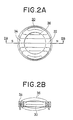
- Figures 2A,2B One preferred example ( Figures 2A,2B) of permanent magnet 30 is shaped as a circular ring and is divided diametrically into two sections, which are magnetized so that the magnetic N-pole 32 is located in one section and the magnetic S-pole 34 is located in the other.
- Lines of magnetic force 36 (indicated in the drawings by solid lines with arrows) extend from the N-pole to the S-pole, mainly in the vacant space within the ring and in the adjoining space. In plan view these lines of force 36 are substantially parallel and are of substantially uniform intensity.
- the circular shape is only one possible shape Square, rectangular, and elliptical shapes may also be suitable.
- the annular magnet with laterally spaced pole sectors may be incorporated in different ways in the apparatus.
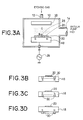
- the magnet 30 is attached to the cathode 18 which faces a grounded anode 38 inside the reactor 10.
- the magnet 30 is mounted on the surface of the cathode 18 facing the anode 38.
- the material to be etched such as a substrate (or wafer) 20, is placed inside the ring of which may surrounf the substrate 20.
- a high-frequency alternating electric field E is produced in the space above the cathode 18, oriented substantially perpendicular to the cathode 18 and, hence the substrate 20.
- This field E interacts with the field B formed between the N- and S-poles of the permanent magnet 30 to induce a magnetron discharge 26 (indicated by dashed circles).
- the plasma intensity in the region of this magnetron discharge 26 is proportional to the intensity of the alternating electric field E and the intensity of the magnetic field B. Since both the alternating electric field E and the magnetic Field B have substantially uniform intensity distributions over the substrate 20, the plasma intensity is also substantially uniform.
- the ionization rate of the magnetron discharge of the plasma is at least two orders of magnitude higher than the ionization rate of an rf discharge.
- the etch rate of the device in this embodiment is therefore at least one order of magnitude higher than in the prior art, and the etching is highly uniform.
- the permanent magnet 30 can be mounted also as shown, for example, in Figs, 3B through 3D. with the permanent magnet 30 embedded in the cathode 18 on the same side as the substrate 20 ( Figure 3B) or embedded in the cathode 18 on the opposite side of the substrate 20 ( Figure 3C) or mounted on the surface of the cathode 18 on the opposite side of the sinstrate 20 ( Figure 3D).
- the permanent magnet can also be mounted at a distance from the cathode 18.
- the permanent magnet is able to generate a substantially uniform, parallel magnetic field orthogonally intersecting an alternating electric field in a suitable region of space inside the reactor adjacent to the substrate.
- the mounting configurations shown in Figures 3B through 3D may improve the flow of etching gas over the substrate surface, as already explained, enabling a highly uniform high-density plasma to be produced by magnetron discharge over the substrate.
- the permanent magnet 30 is situated in the space above the cathode 18 and attached to the anode 38.
- the permanent magnet 30 is mounted on the surface of the anode 38 facing the cathode 18.
- a substantially uniform, parallel magnetic field B orthogonally intersecting an alternating electric field E is generated in the space between the anode 38 and the cathode 18, giving rise to a magnetron discharge in an appropriate region in this space.
- a higher density plasma can be formed by the magnetron discharge 26 in the region adjacent to the substrate surface by reducing the gap between the sanode 38 and cathode 18.
- the flow of etching gas can be improved enabling the high-density plasma produced by the magnetron discharge to be supplied with good uniformity to the material to be etched.
- the permanent magnet 30 can also be mounted on the surface of the anode 38 away from the cathode 18 as in Figure 4B. or can be embedded in the side of the anode 38 near the cathode 18 as in Figure 4D In Figure 4B, the permanent magnet 30 can also be mounted at a distance from the anode 38.
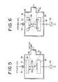
- the permanent magnet 30 is mounted in a space above the cathode 18 by an appropriate means (not shown in the drawing).
- the mutual separation of the cathode 18, the anode 38, and the permanent magnet 30 reduces etching gas turbulence over the surface of the substrate 20, improving the planar distribution of the etch rate and facilitating venting of gas produced by etching, resulting in a higher etch rate.
- the planar uniformity of the etch rate is affected by the electrical potential of the permanent magnet 30, which is hence an important factor.
- the permanent magnet 30 may be tied to the same ground potential as the anode 38, or to the same high frequency potential as the cathode 18, or left at a floating potential in which its only electrical contact is with plasma. The preferred choice is to leave the permanent magnet 30 at a floating potential, if it is desired to minimize distortion of the electric field around the permanent magnet 30.
- one permanent magnet 30 is mounted on the cathode 18 and another similar magnet 40 is mounted on the anode 38, on facing sides thereof.
- the permanent magnets 30 and 40 should preferably be positioned so that their respective S-and N-poles are opposite one another with like poles facing in the same direction.
- the lines of force generated repel each other, creating a more uniform magnetic field above the substrate, enabling a higher plasma density to be achieved. Etching can therefore be performed with greater speed and uniformity.
- the permanent magnets 30 and 40 in this example can also be mounted as shown in Figures 3B through 3D and Figures 4B through 4D.
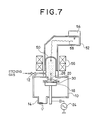
- FIG. 7 and Figure 8 show further embodiments in which the dry etching apparatus uses microwaves to ionize the etching gas to create a plasma.
- the reactor 10 itself is grounded and acts as the cathode.
- the reactor 10 is joined to a quartz tube 50 situated above the cathode 18 and opening into the interior reactor space.
- the quartz tube 50 is inserted into one end of a waveguide 52, the other end of which is equipped with a magnetron 54.
- a solenoid coil 56 surrounds the section of the waveguide 52 containing the quarz tube 50.
- the permanent magnet 30 is a ring, which may be circular and mounted on the same side of the cathode 18 as the substrate.
- the permanent magnet 30 could, however, be mounted in any of the positions shown in Figures 3B through 3D with respect to the cathode.
- the diffuse magnetic field causes the plasma created inside the quartz tube 50 to flow to the substrate 20 to be etched.
- Application of 13.56MHz high-frequency electromagnetic waves to the cathode 18 generates an alternating electric field E oriented perpendicularly to hte substrate 26 in the space over the cathode 18.
- E alternating electric field
- the embodiment shown in Figure 8 differs from the embodiment shown in Figure 7 in that the permanent magnet 30 is located at a distance above the cathode 18, so that the region inside and adjoining the permanent magnet ring is located over the substrate 20.
- the separation of the permanent magnet 30 from the substrate 20 has the effect noted in the third embodiment.
- the positional relation of the permanent magnet 30 and cathode 18 can also be as shown in Figures 3B through 3D.
- the material to be processed is a substrate 20, on which chemically reactive vapor is to be deposited, which is placed in the anode 38, to which the permanent ring magnet shown in Figures 2A and 2B is attached to produce a magnetron discharge.
- the anode 38 and cathode 18 are mounted facing each other inside the reactor 10, and the anode 38 is grounded.
- the permanent magnet 30 is mounted on the surface of the anode 38 near the cathode 18.
- the substrate 20 is located in the vacant permanent magnet 30 which surrounds the substrate 20.
- a high frequency alternating electric field E is generated below the cathode 18, oriented substantially perpendicularly to the anode 38, hence to the chemical vapor-deposition substrate 20.
- a substantially uniform plasma density can again be achieved.
- the reaction products formed in the plasma are deposited in a film.
- a dc bias or a high-frequency (rf) electric field can be applied to the anode 38 if it is desired to vapor-deposit a film while sputtering it with ions.
- FIG. 10B the permanent magnet 30 is located above the surface of the anode 38 on which the substrate is placed; in Fig 10C it is embedded in the anode 38 on the same side as the substrate; in Figure 10D it is embedded in the sanode 38 on the opposite side from the substrate: and in Figure 10F it is located beneath the anode 38 on the opposite side from the substrate.
- the permanent magnet 30 is able to generate a substantially uniform, parallel magnetic field orthogonally intersecting an alternating electric field in a suitable region of space inside the reactor adjacent to the substrate.
- the mounting configurations shown in Figures 10B to 10F may improve the flow of reactant gas over the vapor deposition substrate surface, enabling a highly uniform high-density plasma to be produced by magnetron discharge over the substrate.
- the apparatus shown in Figure 3A to 3D, 4A to 4D, 5. and 6 can be used as a sputtering apparatus by placing the substrate on which sputtered material is to be deposited on the anode and mounting the permanent ring magnet directly on the cathode around the target placed on the cathode and/or the anode to generate a high-density plasma which enables the sputtering deposition process to proceed at a high rate.
- the permanent ring magnet can be mounted a slight distance above the cathode to generate a high-density plasma. This arrangement improves the flow of sputtering gas, enabling a high rate and high uniformity of sputtering deposition.
- the anode can be positioned at a suitable location within the reactor.
- the permanent ring magnet has been situated inside the reactor, but can also be placed outside the reactor. Such a configuration is shown in Figures 9 and 11.
- the permanent ring magnet 42 or 44 should be located in an appropriate position outside the reactor so that the lines of force of the magnetic field B run approximately parallel to the cathode 18 or anode 38 in the space above the cathode 18 or anode 38.
- the permanent magnets were stationary, but the permanent ring magner can be rotated around its center of rotational symmetry or center of gravity in the plane of the ring to rotate the magnetic field in a plane substantially orthogonal to the plane of the alternating electric field. This assists more uniform plasma intensity distribution over the material to be etched, the sputtering target material, or the material on which vapor is to be desposited, leading to greater uniformity of the etch rate, sputter rate, or vapor-deposition rate.
- the permanent magnet may be rotated in any suitable manner. When the permanent magnet is mounted on the cathode or anode, for example, it suffices to provide means of rotating the cathode or anode without rotating the material 20.
- the support structure of the permanent magnet can be used for mechanical rotation control, or the rotation can be controlled electromagnetically from outside the reactor.
- the rate of rotation is not critical.
- the rotation of the two magnets should be synchronized so that their S-and N-poles remain in opposition.
- an arrangement as shown in Figure 18 can be used for rotation of the permanent magnet.
- the arrangement includes a first gear 92 mounting a permanent magnet 42 and a second gear 94 meshing with the first gear 92 which is supported rotatably by a bearing means 96 having a ball bearings arranged circumferentially.
- the second gear is drivable by a shaft 98a of a motor 98 rotating the first and second gear and hence the permanent magnet 42.
- the permanent magnet used can be electrically connected to the high-frequency (rf) power supply or can be electrically grounded to maintain the perpendicular orientation of the electric field (field vector) to the cathode.
- This invention is characterised by the use of a permanent ring magnet to generate the magnetic field necessary to produce a magnetron discharge, and by the positional relationships of the magnet.
- the structure of other parts of the dry process apparatus can be modified to suit the design without being restricted to the structures described above.
- the annular permanent magnet can be used in combination with an auxiliary magnetic member.
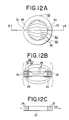
- An example of such a combination is shown in Figures 12A and 12B in which an auxiliary magnetic member 60 in ring-form is disposed inside of and in contact with ring magnet 30 to form a magnet assembly 62.
- the auxiliary magnetic member 30 can be formed integrally with the magnet 30 as shown in Figures 12A and 12B. This can be produced by magnetisation using an external magnetic field Mm of an electromagnet as shown in Figure 12C, to form the N-pole 32 and the S-pole 34 of the main permanent magnet 30. Upon removal of the external magnetic field, the inside parts of the ring adjacent the N-pole 32 and the S-pole 34 of the main permanent magnet 30 are spontaneously magnetized to result in the S-pole 64 and the N-pole 66 of the auxiliary permanent magnet 60.
- the magnet assembly 62 is thus divided into the main permanent magnet 30 and the auxiliary permanent magnet 60, both in the form of a ring. The boundary between the magnet layers 30 and 60 are indicated approximately by the dashed line.
- a suitable material which can be used for the formation of the magnet assembly 60 is alnico containing mainly Al, Ni, Co and Fe.
- the content of Co should preferably be about 30%. With such a high content of Co, the coercive-power is more than about 1,000 Gauss. When the content of Co is about 25%, the coercive-power is less than about 1,000 Gauss and the formation of the N-pole and the S-pole of the auxiliary permanent magnet layer 60 does not occur.
- the lines of magnetic force induced in the central space of the ring will have an improved uniformity as seen in the plan view (Figure 12A) and as seen in cross section ( Figure 12B).
- the lines of magnetic force 68 also have a better parallelism as seen in the cross section ( Figure 12B).
- Figures 13A and 13B show another example of a magnet assembly (members and parts identical to those shown in Figures 12A and 12B are denoted by identical reference numberals) which comprises a main auxiliary permanent magnet 30 and an auxiliary permanent magnet 60 which are separately magnetized and than assembled by fitting magnet 60 in the magnet layer 30, the boundary between them being indicated by a solid line.
- the magnetic field due to the outer magnet layer 30, if taken alone, is more intense than the magnetic field due to the inner axiliary peramnent magnet 60 taken alone.
- the coercive-power of the permanent magnet 30 or 50 is not critical.
- the resultant lines of magnetic force are similar to those of Figures 12A and 12B.
- the auxiliary magnetic member can also be made of a ferromagnetic material having no coercive-force for example iron.
- the assembly is shown in Figures 14A and 14B.
- the part of the auxiliary magnetic member 60 adjacent the N-pole 32 of the permanent magnet 30 is magnetized to exhibit an S-pole 64 on its inner peripheral surface, while the part of the auxiliary magnetic member 60 adjacent the S-pole 34 of the permanent magnet 30 is magnetized to exhibit an N-pole 66 on its peripheral surface.
- the lines of the magnetic force induced by the magnet assembly of Figures 14A and 14B are similar to those shown in Figures 12A, 12B, 13A and 13B, and have an improved uniformity in the central space in the ring as seen in plan view (Fig 14A) and as seem in cross section (Figure 14B).
- the lines of magnetic force 68 also have a better parallelism as seen in the cross sectional view ( Figure 14B).
- the ring permanent magnet and the ring auxiliary magnetic member can be divided into elements arranged with gaps between adjacent pieces, as long as the magnetic property and function of the assembly are maintained. The gaps may be filled with non-magnetic material which does not change the magnetic properties of the assembly.
- Figures 15A and 15B show another example of the magnet assembly (members or parts similar to those in Figures 14A and 4B being denoted by identical reference numberals) in which there is a radial gap between the permanent magnet 30.
- the uniformity and intensity of the magnetic field can be adjusted.
- the vertical position of the auxiliary magnetic member 60 with respect of the magnetic field can also be adjusted.
- the uniformity and intensity of the magnetic field can be also adjusted by differentiating the shape of the auxiliary magnetic member 60 from that of the permanent magnet 30.
- Figures 16A and 16B show another example of the magnet assembly in which an auxiliary magnetic member 70 has a larger outer diameter than the permanent magnet 30, and is positioned beneath the permanent magnet 30.
- the lines of magnetic force 78 deviate downward and the density of the lines of magnetic force 78 in the upper and central regions can be varied, by varying the relative position of the auxiliary magnetic member 70 with respect to permanent magnet 30.
- auxiliary magnetic member 70 can be positioned above the permanent magnet 30.
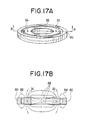
- Figures 17A and 17B show a further example of the magnet assembly.
- an auxiliary magnetic member 80 has a larger diamter than the permanent magnet 30.
- some of the lines of magnetic force 88 circle around the auxiliary magnetic member outside the permanent magnet 30. The intensity of the magnetic field inside the permanent magnet 30 can therefore be varied.
- Figures 16A, 16B, 17A, 17B can be employed to compensate for the difference in the strength of magnetization of the individual permanent magnets, due for example to fluctuation in the conditions under which the individual permanent magnets are fabricated.
- the magnet assembly described above can be used in place of the permanent magnet alone as used in the various embodiments described previously.
- the dry process apparatus of this invention is capable of producing a highly uniform magnetic field in the region inside and adjoining a permanent ring magnet, hence of generating a high-density plasma with a high degree of uniformity over a matrial such as a material to be etched, a target material, or a material on to which vapor is to be deposited.
- the process of etching or sputtering the material or depositing a thin film on it can therefor be accomplished at a high rate with high uniformity. Since the magnetic field produced in the dry process apparatus is oriented essentially parallel to the surface of the material to be processed, electrons in the plasma do not tend to drift onto the material, so that there is less tendency for forming an ion sheath, and the self bias voltage is reduced by a factor of five or more with an attendant reduction in the damage to the material caused by ion bombardment.
- the dry process apparatus of this invention is therefore particularly suited for low-damage etching, for gates that require high vapor-deposition rates, for trench etching, and for deposition of interconnecting materials.
- the dry process apparatus can be of compact construction.
Landscapes
- Chemical & Material Sciences (AREA)
- Engineering & Computer Science (AREA)
- Physics & Mathematics (AREA)
- Plasma & Fusion (AREA)
- Analytical Chemistry (AREA)
- Chemical Kinetics & Catalysis (AREA)
- Materials Engineering (AREA)
- Mechanical Engineering (AREA)
- Metallurgy (AREA)
- Organic Chemistry (AREA)
- Drying Of Semiconductors (AREA)
- Physical Vapour Deposition (AREA)
Applications Claiming Priority (6)
| Application Number | Priority Date | Filing Date | Title |
|---|---|---|---|
| JP14650186 | 1986-06-23 | ||
| JP146501/86 | 1986-06-23 | ||
| JP258535/86 | 1986-10-31 | ||
| JP61258535A JPS6399530A (ja) | 1986-06-23 | 1986-10-31 | ドライプロセス装置 |
| JP17148/87 | 1987-01-29 | ||
| JP62017148A JPH0715900B2 (ja) | 1987-01-29 | 1987-01-29 | ドライプロセス装置 |
Publications (2)
| Publication Number | Publication Date |
|---|---|
| EP0251567A1 true EP0251567A1 (de) | 1988-01-07 |
| EP0251567B1 EP0251567B1 (de) | 1993-09-08 |
Family
ID=27281698
Family Applications (1)
| Application Number | Title | Priority Date | Filing Date |
|---|---|---|---|
| EP87305360A Expired - Lifetime EP0251567B1 (de) | 1986-06-23 | 1987-06-17 | Vorrichtung für ein Trockenverfahren |
Country Status (3)
| Country | Link |
|---|---|
| US (1) | US4842707A (de) |
| EP (1) | EP0251567B1 (de) |
| DE (1) | DE3787328T2 (de) |
Cited By (8)
| Publication number | Priority date | Publication date | Assignee | Title |
|---|---|---|---|---|
| EP0428161A3 (en) * | 1989-11-15 | 1991-07-31 | Kokusai Electric Co., Ltd. | Dry process system |
| EP0479189A1 (de) * | 1990-09-29 | 1992-04-08 | Tokyo Electron Limited | Gerät zur Magnetronplasmabearbeitung |
| EP0482891A3 (en) * | 1990-10-22 | 1992-06-17 | Varian Associates, Inc. | High vacuum magnetron sputter source |
| US5162633A (en) * | 1988-06-29 | 1992-11-10 | Hitachi, Ltd. | Microwave-excited plasma processing apparatus |
| US5228950A (en) * | 1990-12-04 | 1993-07-20 | Applied Materials, Inc. | Dry process for removal of undesirable oxide and/or silicon residues from semiconductor wafer after processing |
| EP0639939A1 (de) * | 1993-08-20 | 1995-02-22 | Ebara Corporation | Quelle für schnelle Atomstrahlen |
| EP0644273B1 (de) * | 1993-09-16 | 2000-07-19 | Applied Materials, Inc. | Vorrichtung zur Magnetron-Plasma-Aufstäube-Beschichtung und Verfahren zum Aufstäube-Beschichten eines Substrates |
| CN115386850A (zh) * | 2022-08-30 | 2022-11-25 | 上海积塔半导体有限公司 | 磁控溅射沉积装置 |
Families Citing this family (29)
| Publication number | Priority date | Publication date | Assignee | Title |
|---|---|---|---|---|
| US4983253A (en) * | 1988-05-27 | 1991-01-08 | University Of Houston-University Park | Magnetically enhanced RIE process and apparatus |
| JPH0215174A (ja) * | 1988-07-01 | 1990-01-18 | Canon Inc | マイクロ波プラズマcvd装置 |
| US4950377A (en) * | 1988-09-23 | 1990-08-21 | Siemens Aktiengesellschaft | Apparatus and method for reactive ion etching |
| US5032205A (en) * | 1989-05-05 | 1991-07-16 | Wisconsin Alumni Research Foundation | Plasma etching apparatus with surface magnetic fields |
| JP3033104B2 (ja) * | 1989-11-17 | 2000-04-17 | ソニー株式会社 | エッチング方法 |
| US5289152A (en) * | 1990-09-19 | 1994-02-22 | Tdk Corporation | Permanent magnet magnetic circuit |
| JP3170319B2 (ja) * | 1991-08-20 | 2001-05-28 | 東京エレクトロン株式会社 | マグネトロンプラズマ処理装置 |
| US5224441A (en) * | 1991-09-27 | 1993-07-06 | The Boc Group, Inc. | Apparatus for rapid plasma treatments and method |
| US5849136A (en) * | 1991-10-11 | 1998-12-15 | Applied Materials, Inc. | High frequency semiconductor wafer processing apparatus and method |
| JP3065781B2 (ja) * | 1992-03-09 | 2000-07-17 | ティーディーケイ株式会社 | 永久磁石磁気回路 |
| DE4310258A1 (de) * | 1993-03-30 | 1994-10-06 | Bosch Gmbh Robert | Vorrichtung zur Herstellung einer Plasmapolymerschutzschicht auf Werkstücken, insbesondere Scheinwerferreflektoren |
| US6022446A (en) * | 1995-08-21 | 2000-02-08 | Shan; Hongching | Shallow magnetic fields for generating circulating electrons to enhance plasma processing |
| TW303480B (en) * | 1996-01-24 | 1997-04-21 | Applied Materials Inc | Magnetically confined plasma reactor for processing a semiconductor wafer |
| US5868897A (en) * | 1996-07-31 | 1999-02-09 | Toyo Technologies, Inc. | Device and method for processing a plasma to alter the surface of a substrate using neutrals |
| US5993678A (en) * | 1996-07-31 | 1999-11-30 | Toyo Technologies Inc. | Device and method for processing a plasma to alter the surface of a substrate |
| US6051151A (en) * | 1997-11-12 | 2000-04-18 | International Business Machines Corporation | Apparatus and method of producing a negative ion plasma |
| US6863835B1 (en) | 2000-04-25 | 2005-03-08 | James D. Carducci | Magnetic barrier for plasma in chamber exhaust |
| DE10156615B4 (de) * | 2001-11-17 | 2004-10-07 | Forschungszentrum Karlsruhe Gmbh | Einrichtung zur Erzeugung eines örtlich variierbaren Elektron-Zyklotron-Resonanz-Mikrowellen-Niederdruckplasmas |
| US20040028837A1 (en) * | 2002-06-28 | 2004-02-12 | Tokyo Electron Limited | Method and apparatus for plasma processing |
| US7059268B2 (en) * | 2002-12-20 | 2006-06-13 | Tokyo Electron Limited | Method, apparatus and magnet assembly for enhancing and localizing a capacitively coupled plasma |
| WO2005009605A1 (ja) * | 2003-07-24 | 2005-02-03 | Ryoichi Aogaki | 磁気障壁により形成されたマイクロリアクタ |
| JP4527431B2 (ja) * | 2004-04-08 | 2010-08-18 | 東京エレクトロン株式会社 | プラズマ処理装置 |
| US8697198B2 (en) * | 2011-03-31 | 2014-04-15 | Veeco Ald Inc. | Magnetic field assisted deposition |
| US20130026136A1 (en) * | 2011-07-29 | 2013-01-31 | Qualcomm Mems Technologies, Inc. | Sputter-etch tool and liners |
| US20130240147A1 (en) * | 2012-03-19 | 2013-09-19 | Sang Ki Nam | Methods and apparatus for selectively modulating azimuthal non-uniformity in a plasma processing system |
| JP6284825B2 (ja) * | 2014-05-19 | 2018-02-28 | 東京エレクトロン株式会社 | プラズマ処理装置 |
| US11572618B2 (en) * | 2019-08-27 | 2023-02-07 | Applied Materials, Inc. | Method and chamber for backside physical vapor deposition |
| US12020898B2 (en) * | 2019-09-09 | 2024-06-25 | Tokyo Electron Limited | Plasma processing system and method of processing substrate |
| US11787008B2 (en) * | 2020-12-18 | 2023-10-17 | Applied Materials, Inc. | Chemical mechanical polishing with applied magnetic field |
Citations (12)
| Publication number | Priority date | Publication date | Assignee | Title |
|---|---|---|---|---|
| DE3206413A1 (de) * | 1982-02-23 | 1983-09-01 | Siemens AG, 1000 Berlin und 8000 München | Verfahren zum herstellen von aus silizium oder aus siliziden hochschmelzender metalle bestehenden schichten unter verwendung einer planar-magnetron-zerstaeubungsanlage |
| DE3322680A1 (de) * | 1982-06-25 | 1984-01-05 | Hitachi, Ltd., Tokyo | Verfahren zum aufwachsenlassen eines silizium enthaltenden films durch plasmaablagerung |
| EP0136450A1 (de) * | 1983-09-15 | 1985-04-10 | Robert Bosch Gmbh | Verfahren zum Herstellen einer Spiegelschicht, insbesondere für Scheinwerferreflektoren |
| EP0154158A1 (de) * | 1984-02-02 | 1985-09-11 | Hitachi Metals, Ltd. | Verfahren zur Herstellung magnetischer Aufzeichnungsträger |
| AT378971B (de) * | 1981-03-02 | 1985-10-25 | Leybold Heraeus Gmbh & Co Kg | Verfahren und vorrichtung zum beschichten von formteilen durch katodenzerstaeubung |
| EP0162643A1 (de) * | 1984-05-17 | 1985-11-27 | Varian Associates, Inc. | Zerstäubungs-Beschichtungs-Quelle mit mehreren ringförmigen Auftreffplatten |
| EP0162642A1 (de) * | 1984-05-17 | 1985-11-27 | Varian Associates, Inc. | Magnetron-Zerstäubungs-Vorrichtung, welche dasselbe Polstück zur Ankopplung von einzelnen, begrenzenden magnetischen Feldern an Auftreffplatten, die getrennten Entladungen ausgesetzt sind, verwendet |
| DD230565A3 (de) * | 1983-11-03 | 1985-12-04 | Johannes Hartung | Plasmatron-quelle |
| EP0163445A1 (de) * | 1984-05-17 | 1985-12-04 | Varian Associates, Inc. | Magnetron-Zerstäubungs-Vorrichtung mit ebenen und konkaven Auftreffplatten |
| EP0168446A1 (de) * | 1984-01-17 | 1986-01-22 | LEHA HANDELSGESELLSCHAFT MbH. & CO. | Verfahren zur herstellung von wärmebeständigen verpackungen |
| EP0173164A1 (de) * | 1984-08-31 | 1986-03-05 | Hitachi, Ltd. | Aufstäuben mittels Mikrowellen |
| DE3434698A1 (de) * | 1984-09-21 | 1986-04-03 | The University Of British Columbia, Vancouver, British Columbia | Planarmagnetron-sputtereinrichtung |
Family Cites Families (13)
| Publication number | Priority date | Publication date | Assignee | Title |
|---|---|---|---|---|
| US4155825A (en) * | 1977-05-02 | 1979-05-22 | Fournier Paul R | Integrated sputtering apparatus and method |
| US4325776A (en) * | 1977-06-20 | 1982-04-20 | Siemens Aktiengesellschaft | Method for preparing coarse-crystal or single-crystal metal films |
| US4461688A (en) * | 1980-06-23 | 1984-07-24 | Vac-Tec Systems, Inc. | Magnetically enhanced sputtering device having a plurality of magnetic field sources including improved plasma trapping device and method |
| US4404077A (en) * | 1981-04-07 | 1983-09-13 | Fournier Paul R | Integrated sputtering apparatus and method |
| US4434037A (en) * | 1981-07-16 | 1984-02-28 | Ampex Corporation | High rate sputtering system and method |
| US4466872A (en) * | 1982-12-23 | 1984-08-21 | At&T Technologies, Inc. | Methods of and apparatus for depositing a continuous film of minimum thickness |
| US4581118A (en) * | 1983-01-26 | 1986-04-08 | Materials Research Corporation | Shaped field magnetron electrode |
| JPH0627323B2 (ja) * | 1983-12-26 | 1994-04-13 | 株式会社日立製作所 | スパツタリング方法及びその装置 |
| US4486287A (en) * | 1984-02-06 | 1984-12-04 | Fournier Paul R | Cross-field diode sputtering target assembly |
| US4595482A (en) * | 1984-05-17 | 1986-06-17 | Varian Associates, Inc. | Apparatus for and the method of controlling magnetron sputter device having separate confining magnetic fields to separate targets subject to separate discharges |
| KR900005347B1 (ko) * | 1984-09-19 | 1990-07-27 | 가부시기가이샤 히다찌세이사꾸쇼 | 플라즈마 처리장치 |
| JPS6274073A (ja) * | 1985-09-26 | 1987-04-04 | Hitachi Ltd | スパツタ装置 |
| US4668338A (en) * | 1985-12-30 | 1987-05-26 | Applied Materials, Inc. | Magnetron-enhanced plasma etching process |
-
1987
- 1987-06-15 US US07/062,185 patent/US4842707A/en not_active Expired - Lifetime
- 1987-06-17 DE DE87305360T patent/DE3787328T2/de not_active Expired - Fee Related
- 1987-06-17 EP EP87305360A patent/EP0251567B1/de not_active Expired - Lifetime
Patent Citations (12)
| Publication number | Priority date | Publication date | Assignee | Title |
|---|---|---|---|---|
| AT378971B (de) * | 1981-03-02 | 1985-10-25 | Leybold Heraeus Gmbh & Co Kg | Verfahren und vorrichtung zum beschichten von formteilen durch katodenzerstaeubung |
| DE3206413A1 (de) * | 1982-02-23 | 1983-09-01 | Siemens AG, 1000 Berlin und 8000 München | Verfahren zum herstellen von aus silizium oder aus siliziden hochschmelzender metalle bestehenden schichten unter verwendung einer planar-magnetron-zerstaeubungsanlage |
| DE3322680A1 (de) * | 1982-06-25 | 1984-01-05 | Hitachi, Ltd., Tokyo | Verfahren zum aufwachsenlassen eines silizium enthaltenden films durch plasmaablagerung |
| EP0136450A1 (de) * | 1983-09-15 | 1985-04-10 | Robert Bosch Gmbh | Verfahren zum Herstellen einer Spiegelschicht, insbesondere für Scheinwerferreflektoren |
| DD230565A3 (de) * | 1983-11-03 | 1985-12-04 | Johannes Hartung | Plasmatron-quelle |
| EP0168446A1 (de) * | 1984-01-17 | 1986-01-22 | LEHA HANDELSGESELLSCHAFT MbH. & CO. | Verfahren zur herstellung von wärmebeständigen verpackungen |
| EP0154158A1 (de) * | 1984-02-02 | 1985-09-11 | Hitachi Metals, Ltd. | Verfahren zur Herstellung magnetischer Aufzeichnungsträger |
| EP0162643A1 (de) * | 1984-05-17 | 1985-11-27 | Varian Associates, Inc. | Zerstäubungs-Beschichtungs-Quelle mit mehreren ringförmigen Auftreffplatten |
| EP0162642A1 (de) * | 1984-05-17 | 1985-11-27 | Varian Associates, Inc. | Magnetron-Zerstäubungs-Vorrichtung, welche dasselbe Polstück zur Ankopplung von einzelnen, begrenzenden magnetischen Feldern an Auftreffplatten, die getrennten Entladungen ausgesetzt sind, verwendet |
| EP0163445A1 (de) * | 1984-05-17 | 1985-12-04 | Varian Associates, Inc. | Magnetron-Zerstäubungs-Vorrichtung mit ebenen und konkaven Auftreffplatten |
| EP0173164A1 (de) * | 1984-08-31 | 1986-03-05 | Hitachi, Ltd. | Aufstäuben mittels Mikrowellen |
| DE3434698A1 (de) * | 1984-09-21 | 1986-04-03 | The University Of British Columbia, Vancouver, British Columbia | Planarmagnetron-sputtereinrichtung |
Cited By (13)
| Publication number | Priority date | Publication date | Assignee | Title |
|---|---|---|---|---|
| US5162633A (en) * | 1988-06-29 | 1992-11-10 | Hitachi, Ltd. | Microwave-excited plasma processing apparatus |
| EP0428161A3 (en) * | 1989-11-15 | 1991-07-31 | Kokusai Electric Co., Ltd. | Dry process system |
| US5660671A (en) * | 1990-09-29 | 1997-08-26 | Tokyo Electron Limited | Magnetron plasma processing apparatus and processing method |
| US5376211A (en) * | 1990-09-29 | 1994-12-27 | Tokyo Electron Limited | Magnetron plasma processing apparatus and processing method |
| EP0663683A3 (de) * | 1990-09-29 | 1995-10-25 | Tokyo Electron Ltd | Magnetron-Plasma-Bearbeitungsgerät und Bearbeitungsverfahren. |
| EP0479189A1 (de) * | 1990-09-29 | 1992-04-08 | Tokyo Electron Limited | Gerät zur Magnetronplasmabearbeitung |
| EP0482891A3 (en) * | 1990-10-22 | 1992-06-17 | Varian Associates, Inc. | High vacuum magnetron sputter source |
| US5228950A (en) * | 1990-12-04 | 1993-07-20 | Applied Materials, Inc. | Dry process for removal of undesirable oxide and/or silicon residues from semiconductor wafer after processing |
| EP0639939A1 (de) * | 1993-08-20 | 1995-02-22 | Ebara Corporation | Quelle für schnelle Atomstrahlen |
| US5519213A (en) * | 1993-08-20 | 1996-05-21 | Ebara Corporation | Fast atom beam source |
| EP0644273B1 (de) * | 1993-09-16 | 2000-07-19 | Applied Materials, Inc. | Vorrichtung zur Magnetron-Plasma-Aufstäube-Beschichtung und Verfahren zum Aufstäube-Beschichten eines Substrates |
| CN115386850A (zh) * | 2022-08-30 | 2022-11-25 | 上海积塔半导体有限公司 | 磁控溅射沉积装置 |
| CN115386850B (zh) * | 2022-08-30 | 2023-12-29 | 上海积塔半导体有限公司 | 磁控溅射沉积装置 |
Also Published As
| Publication number | Publication date |
|---|---|
| EP0251567B1 (de) | 1993-09-08 |
| US4842707A (en) | 1989-06-27 |
| DE3787328T2 (de) | 1994-02-24 |
| DE3787328D1 (de) | 1993-10-14 |
Similar Documents
| Publication | Publication Date | Title |
|---|---|---|
| EP0251567B1 (de) | Vorrichtung für ein Trockenverfahren | |
| JP4025193B2 (ja) | プラズマ生成装置、それを有するエッチング装置およびイオン物理蒸着装置、プラズマにエネルギを誘導結合するrfコイルおよびプラズマ生成方法 | |
| US4960073A (en) | Microwave plasma treatment apparatus | |
| KR100659828B1 (ko) | 이온화 물리적 증착 방법 및 장치 | |
| US4987346A (en) | Particle source for a reactive ion beam etching or plasma deposition installation | |
| US5122252A (en) | Arrangement for the coating of substrates | |
| KR100646266B1 (ko) | 스퍼터링 증착용 플라스마 처리 장치 | |
| US6143140A (en) | Method and apparatus to improve the side wall and bottom coverage in IMP process by using magnetic field | |
| JP3730867B2 (ja) | プラズマ蒸着法並びに磁気バケットおよび同心プラズマおよび材料源を備える装置 | |
| CN1324641C (zh) | 用于等离子体溅射的与旋转磁控管结合的磁体阵列 | |
| EP0148504B2 (de) | Verfahren und Vorrichtung zur Zerstäubung | |
| KR100786713B1 (ko) | 스퍼터링 반응기 및 비균형 마그네트론의 이용 방법 | |
| CA1195951A (en) | Shaped field magnetron electrode | |
| KR0127663B1 (ko) | 플라즈마발생장치 및 플라즈마발생방법 | |
| US5369337A (en) | DC or HF ion source | |
| US6761804B2 (en) | Inverted magnetron | |
| US5397448A (en) | Device for generating a plasma by means of cathode sputtering and microwave-irradiation | |
| KR20090037343A (ko) | 자화된 유도결합형 플라즈마 처리장치 및 플라즈마 발생방법 | |
| JPH11283926A (ja) | プラズマ処理装置 | |
| WO2000003055A1 (en) | Shield for ionized physical vapor deposition apparatus | |
| KR910000507B1 (ko) | 드라이 프로세스장치 | |
| JPH0715900B2 (ja) | ドライプロセス装置 | |
| JPH04276069A (ja) | スパッタリング方法およびその装置 | |
| JP2001220671A (ja) | スパッタ成膜応用のためのプラズマ処理装置 | |
| JPS63276226A (ja) | ドライプロセス装置 |
Legal Events
| Date | Code | Title | Description |
|---|---|---|---|
| PUAI | Public reference made under article 153(3) epc to a published international application that has entered the european phase |
Free format text: ORIGINAL CODE: 0009012 |
|
| AK | Designated contracting states |
Kind code of ref document: A1 Designated state(s): DE FR GB |
|
| 17P | Request for examination filed |
Effective date: 19880125 |
|
| 17Q | First examination report despatched |
Effective date: 19900723 |
|
| GRAA | (expected) grant |
Free format text: ORIGINAL CODE: 0009210 |
|
| AK | Designated contracting states |
Kind code of ref document: B1 Designated state(s): DE FR GB |
|
| ET | Fr: translation filed | ||
| REF | Corresponds to: |
Ref document number: 3787328 Country of ref document: DE Date of ref document: 19931014 |
|
| PLBE | No opposition filed within time limit |
Free format text: ORIGINAL CODE: 0009261 |
|
| STAA | Information on the status of an ep patent application or granted ep patent |
Free format text: STATUS: NO OPPOSITION FILED WITHIN TIME LIMIT |
|
| 26N | No opposition filed | ||
| PGFP | Annual fee paid to national office [announced via postgrant information from national office to epo] |
Ref country code: GB Payment date: 19980608 Year of fee payment: 12 |
|
| PGFP | Annual fee paid to national office [announced via postgrant information from national office to epo] |
Ref country code: FR Payment date: 19980609 Year of fee payment: 12 |
|
| PGFP | Annual fee paid to national office [announced via postgrant information from national office to epo] |
Ref country code: DE Payment date: 19980629 Year of fee payment: 12 |
|
| PG25 | Lapsed in a contracting state [announced via postgrant information from national office to epo] |
Ref country code: GB Free format text: LAPSE BECAUSE OF NON-PAYMENT OF DUE FEES Effective date: 19990617 |
|
| PG25 | Lapsed in a contracting state [announced via postgrant information from national office to epo] |
Ref country code: FR Free format text: THE PATENT HAS BEEN ANNULLED BY A DECISION OF A NATIONAL AUTHORITY Effective date: 19990630 |
|
| GBPC | Gb: european patent ceased through non-payment of renewal fee |
Effective date: 19990617 |
|
| PG25 | Lapsed in a contracting state [announced via postgrant information from national office to epo] |
Ref country code: DE Free format text: LAPSE BECAUSE OF NON-PAYMENT OF DUE FEES Effective date: 20000503 |
|
| REG | Reference to a national code |
Ref country code: FR Ref legal event code: ST |