EP0252929B1 - Elektrisch veränderbarer piezoelektrischer hybrid-kondensator - Google Patents
Elektrisch veränderbarer piezoelektrischer hybrid-kondensator Download PDFInfo
- Publication number
- EP0252929B1 EP0252929B1 EP86907174A EP86907174A EP0252929B1 EP 0252929 B1 EP0252929 B1 EP 0252929B1 EP 86907174 A EP86907174 A EP 86907174A EP 86907174 A EP86907174 A EP 86907174A EP 0252929 B1 EP0252929 B1 EP 0252929B1
- Authority
- EP
- European Patent Office
- Prior art keywords
- piezoelectric
- capacitor
- ridge
- wafer
- plate
- Prior art date
- Legal status (The legal status is an assumption and is not a legal conclusion. Google has not performed a legal analysis and makes no representation as to the accuracy of the status listed.)
- Expired - Lifetime
Links
- 239000003990 capacitor Substances 0.000 title claims abstract description 105
- 239000000758 substrate Substances 0.000 claims abstract description 39
- 238000004377 microelectronic Methods 0.000 claims abstract description 27
- 238000000034 method Methods 0.000 claims description 23
- 239000003989 dielectric material Substances 0.000 claims description 8
- 239000010409 thin film Substances 0.000 abstract description 7
- 238000005516 engineering process Methods 0.000 abstract description 4
- 238000004519 manufacturing process Methods 0.000 description 8
- 239000004593 Epoxy Substances 0.000 description 4
- 239000004020 conductor Substances 0.000 description 4
- 239000010408 film Substances 0.000 description 4
- 238000005476 soldering Methods 0.000 description 4
- 239000000919 ceramic Substances 0.000 description 3
- 230000003247 decreasing effect Effects 0.000 description 3
- 239000011521 glass Substances 0.000 description 3
- 238000000926 separation method Methods 0.000 description 3
- VYPSYNLAJGMNEJ-UHFFFAOYSA-N Silicium dioxide Chemical compound O=[Si]=O VYPSYNLAJGMNEJ-UHFFFAOYSA-N 0.000 description 2
- PNEYBMLMFCGWSK-UHFFFAOYSA-N aluminium oxide Inorganic materials [O-2].[O-2].[O-2].[Al+3].[Al+3] PNEYBMLMFCGWSK-UHFFFAOYSA-N 0.000 description 2
- 229910000679 solder Inorganic materials 0.000 description 2
- RYGMFSIKBFXOCR-UHFFFAOYSA-N Copper Chemical compound [Cu] RYGMFSIKBFXOCR-UHFFFAOYSA-N 0.000 description 1
- BQCADISMDOOEFD-UHFFFAOYSA-N Silver Chemical compound [Ag] BQCADISMDOOEFD-UHFFFAOYSA-N 0.000 description 1
- 229910010293 ceramic material Inorganic materials 0.000 description 1
- 229910052681 coesite Inorganic materials 0.000 description 1
- 230000006835 compression Effects 0.000 description 1
- 238000007906 compression Methods 0.000 description 1
- 229910052802 copper Inorganic materials 0.000 description 1
- 239000010949 copper Substances 0.000 description 1
- 229910052906 cristobalite Inorganic materials 0.000 description 1
- 230000007423 decrease Effects 0.000 description 1
- 238000009713 electroplating Methods 0.000 description 1
- 238000005530 etching Methods 0.000 description 1
- 238000010304 firing Methods 0.000 description 1
- PCHJSUWPFVWCPO-UHFFFAOYSA-N gold Chemical compound [Au] PCHJSUWPFVWCPO-UHFFFAOYSA-N 0.000 description 1
- 229910052737 gold Inorganic materials 0.000 description 1
- 239000010931 gold Substances 0.000 description 1
- 238000010438 heat treatment Methods 0.000 description 1
- 239000012212 insulator Substances 0.000 description 1
- 239000000463 material Substances 0.000 description 1
- 230000010287 polarization Effects 0.000 description 1
- 229920001721 polyimide Polymers 0.000 description 1
- -1 resistors Substances 0.000 description 1
- 238000012216 screening Methods 0.000 description 1
- 239000000377 silicon dioxide Substances 0.000 description 1
- 235000012239 silicon dioxide Nutrition 0.000 description 1
- 229910052709 silver Inorganic materials 0.000 description 1
- 239000004332 silver Substances 0.000 description 1
- 230000003595 spectral effect Effects 0.000 description 1
- 238000004544 sputter deposition Methods 0.000 description 1
- 229910052682 stishovite Inorganic materials 0.000 description 1
- 229910052905 tridymite Inorganic materials 0.000 description 1
- 238000001771 vacuum deposition Methods 0.000 description 1
Images


Classifications
-
- H—ELECTRICITY
- H01—ELECTRIC ELEMENTS
- H01G—CAPACITORS; CAPACITORS, RECTIFIERS, DETECTORS, SWITCHING DEVICES, LIGHT-SENSITIVE OR TEMPERATURE-SENSITIVE DEVICES OF THE ELECTROLYTIC TYPE
- H01G5/00—Capacitors in which the capacitance is varied by mechanical means, e.g. by turning a shaft; Processes of their manufacture
- H01G5/16—Capacitors in which the capacitance is varied by mechanical means, e.g. by turning a shaft; Processes of their manufacture using variation of distance between electrodes
-
- H—ELECTRICITY
- H01—ELECTRIC ELEMENTS
- H01G—CAPACITORS; CAPACITORS, RECTIFIERS, DETECTORS, SWITCHING DEVICES, LIGHT-SENSITIVE OR TEMPERATURE-SENSITIVE DEVICES OF THE ELECTROLYTIC TYPE
- H01G5/00—Capacitors in which the capacitance is varied by mechanical means, e.g. by turning a shaft; Processes of their manufacture
- H01G5/16—Capacitors in which the capacitance is varied by mechanical means, e.g. by turning a shaft; Processes of their manufacture using variation of distance between electrodes
- H01G5/18—Capacitors in which the capacitance is varied by mechanical means, e.g. by turning a shaft; Processes of their manufacture using variation of distance between electrodes due to change in inclination, e.g. by flexing, by spiral wrapping
-
- Y—GENERAL TAGGING OF NEW TECHNOLOGICAL DEVELOPMENTS; GENERAL TAGGING OF CROSS-SECTIONAL TECHNOLOGIES SPANNING OVER SEVERAL SECTIONS OF THE IPC; TECHNICAL SUBJECTS COVERED BY FORMER USPC CROSS-REFERENCE ART COLLECTIONS [XRACs] AND DIGESTS
- Y10—TECHNICAL SUBJECTS COVERED BY FORMER USPC
- Y10T—TECHNICAL SUBJECTS COVERED BY FORMER US CLASSIFICATION
- Y10T29/00—Metal working
- Y10T29/42—Piezoelectric device making
-
- Y—GENERAL TAGGING OF NEW TECHNOLOGICAL DEVELOPMENTS; GENERAL TAGGING OF CROSS-SECTIONAL TECHNOLOGIES SPANNING OVER SEVERAL SECTIONS OF THE IPC; TECHNICAL SUBJECTS COVERED BY FORMER USPC CROSS-REFERENCE ART COLLECTIONS [XRACs] AND DIGESTS
- Y10—TECHNICAL SUBJECTS COVERED BY FORMER USPC
- Y10T—TECHNICAL SUBJECTS COVERED BY FORMER US CLASSIFICATION
- Y10T29/00—Metal working
- Y10T29/43—Electric condenser making
Definitions
- This invention relates to the field of electrical capacitors and more particularly to electrically variable piezoelectric capacitors manufacturable on thick or thin film hybrid microelectronic circuit substrates.
- Hybrid microelectronic circuits are typically manufactured using either a thick film or a thin film process.
- conductors, resistors, dielectrics, and insulators are silk screened onto a thin ceramic substrate, dried, and fired. Solder paste is then screened on at appropriate locations and discrete parts are attached to the substrate by heating the substrate and reflowing the solder.
- conductors are formed by applying a conductive material to the substrate surface and then etching the surface at predetermined locations using a photolithgraphic process.
- a varactor diode is normally used because of its small size and ease of attachment to a hybrid microelectronic circuit substrate.
- Varactor diodes have disadvantages, however, the most significant is their nonlinear voltage-capacitance response. It is a well known principle that nonlinear devices generate harmonic frequencies. In radio circuits, where the spectral purity of the transmitted signal is extremely important, any nonlinear device can generate unwanted harmonics which can be unintentionally amplified and transmitted. Thus, when varactor diodes are used in radio circuits, extreme care must be taken to insure that any harmonic frequencies that they generate are not radiated.
- varactor diodes and other nonlinear capacitors are two terminal devices. Therefore, the capacitance control voltage and the signal voltage cannot be separate and isolated voltages, but must be applied across the same two terminals. Therefore, the signal voltage must be combined with the control voltage.
- a typical prior art piezoelectric variable capacitor such as that disclosed in US-A 3,949,246 includes two bimorph piezoelectric elements. Each element includes two piezoelectric layers of different polarizations bonded together with a conductive control plate in between the layers. One surface of each element has a conductive control plate while the other surface has a centrally located capacitor plate with a lead extending to the edge of the element. Each capacitor plate is surrounded by a narrow insulating area which in turn is surrounded by another control plate. The two elements are then bonded together at their capacitor plate surfaces. A control voltage, appropriately applied to the various control plates, causes the elements to flex at their centers thereby moving the two capacitor plates further apart and varying the capacitance accordingly.
- An object of the present invention is to provide an improved electrically variable piezoelectric capacitor.
- a more specific object of the present invention is to provide an electrically variable piezoelectric capacitor that can be manufactured on hybrid microelectronic circuit substrates using existing hybrid microelectronic circuit manufacturing technology.
- a method of constructing an electrically variable piezoelectric hybrid microelectronic circuit capacitor comprising the steps of: forming a first capacitor plate on a surface of a substrate; forming a ridge on said surface of said substrate substantially about said first capacitor plate with the upper surface of said ridge above said first capacitor plate; forming a second capacitor plate on a first surface of a piezoelectric wafer; forming a first control plate on a second surface of said piezoelectric wafer; and attaching said piezoelectric wafer to said ridge whereby said second capacitor plate is located substantially opposite said first capacitor plate.
- an electronically variable piezoelectric hybrid microelectronic circuit capacitor comprising in combination: a substrate; a first capacitor plate formed on a surface of said substrate; a ridge on said surface of said substrate substantially about said first capacitor plate, said ridge having an upper surface extending above said first capacitor plate; a piezoelectric wafer connected to said upper surface of said ridge; a second capacitor plate formed on a first surface of said piezoelectric wafer; and a first control plate formed on a second surface of said piezoelectric wafer.
- an electrically variable piezoelectric hybrid microelectronic circuit capacitor in still another embodiment, includes a ceramic substrate with a first capacitor plate and a substantially circular supporting ridge formed on one surface of the ceramic substrate.
- the ridge which is formed by a hybrid microelectronic circuit manufacturing process, has an upper surface positioned a predetermined distance above the first capacitor plate.
- a substantially dome shaped piezoelectric wafer which has a convex surface adjacent the first capacitor plate and an opposing concave surface, is connected at its perimeter to the upper surface of the ridge.
- a second capacitor plate and a control plate are respectively formed on the convex and concave surfaces of the piezoelectric wafer. The capacitance between the first and second capacitor plates depends on the control voltage applied between the control plate and the second capacitor plate.
- FIG. 1 is a top view of the preferred three terminal monomorphic embodiment of the present invention wherein the capacitance control voltage V c and the output capacitance C o are illustrated schematically.
- FIG. 2 is a sectional view of the preferred three terminal monomorphic embodiment as seen along line 2-2 of FIG. 1.
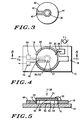
- FIG. 3 is a bottom view of the preferred piezoelectric element as used in the four terminal embodiment: of FIGS. 4-5 and 8-9.
- FIG. 4 is a top view of the preferred four terminal monomorphic embodiment of the present invention wherein the capacitance control voltage V c and the output capacitance C o are illustrated schematically.
- FIG. 5 is a sectional view of the preferred four terminal monomorphic embodiment as seen along line 5-5 of FIG. 4.
- FIG. 6 is a top view of the preferred three terminal bimorphic embodiment of the present invention wherein the capacitance control voltage V c and the output capacitance C o are illustrated schematically.
- FIG. 7 is sectional view of the preferred three terminal bimorphic embodiment as seen along line 7-7 of FIG. 6.
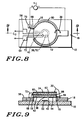
- FIG. 8 is a top view of the preferred four terminal bimorphic embodiment of the present invention wherein the capacitance control voltage V c and the output capacitance C o are illustrated schematically.
- FIG. 9 is a sectional view of the preferred four terminal bimorphic embodiment as seen along line 9-9 of FIG. 8.
- FIGs. 1 and 2 illustrate the preferred three terminal monomorphic embodiment of the present invention.
- a hybrid microelectronic circuit substrate 10 is preferably made from a ceramic material, such as alumina, although any well known material compatible with hybrid microelectronic circuit manufacturing processes is suitable.
- a first capacitor plate 12, having an attached terminal 14, is formed on one surface of substrate 10 by a well known hybrid microelectronic circuit manufacturing process for forming conductive layers. Such well known processes include silk screening for thick film circuits and sputtering, vacuum deposition, or electroplating for thin film circuits.
- the preferred thickness for first capacitor plate 12 and terminal 14 is 25 to 50 ⁇ m (microns).
- a ridge 16, having an attached terminal 18, is also formed on the surface of substrate 10 by a well known hybrid microelectronic circuit manufacturing process.
- ridge 16 can also be formed by tooling substrate 10.
- ridge 16 can be formed by a tool die when the alumina substrate 10 is "green”. After firing, ridge 16 and terminal 18 would then be permanently formed on the surface of substrate 10.
- Ridge 16 and terminal 18 can also be comprised of a preformed glass ring epoxy bonded to the surface of substrate 10. If ridge 16 is tooled or preformed glass, a conductive surface can then be applied to its upper surface by one of the aforementioned processes for forming conductive layers.
- This conductive surface on ridge 16 and terminal 18 is preferably applied simultaneously with first capacitor plate 12. Regardless of the process used to form ridge 16, its upper surface is always a predetermined distance above the upper surface of capacitor plate 12 and terminal 14. This distance provides for separation between the two capacitor plates and is preferably less than 25 microns, although wider capacitor plate separations are acceptable.
- a well known monomorphic piezoelectric wafer 20 has a second capacitor plate 22 formed on its lower surface and a control plate 24 formed on its upper surface. Capacitor plate 22 and control plate 24 are preferably electroplated on piezoelectric wafer 20, although any hybrid microelectronic circuit process for forming conductive layers is suitable. Piezoelectric wafer 20 is bonded to ridge 16 at capacitor plate 22, preferably by soldering, however other well known methods of providing a conductive bond, such as conductive epoxy, are suitable. Prior to bonding, a force 26 is applied substantially in the center of piezoelectric wafer 20 causing the wafer to arch downward slightly.
- the amount of the force will depend on the particular piezoelectric wafer used, it should be sufficient to produce about a 13 ⁇ m (micron) deflection at the center of wafer 20.
- force 26 is removed and wafer 20 will maintain a slight arched or domed shape, curving in the direction of first capacitor plate 12.
- Fixing a slight but permanent arch into wafer 20 is necessary to predispose wafer 20 to flex downwards towards first capacitor plate 12 when a control voltage is applied between control plate 24 and second capacitor plate 22. Without this predisposition to move downward, monomorphic piezoelectric wafer 20 would have an equal probability of flexing away from first capacitor plate 12 when the control voltage V c is applied.
- Capacitance control terminal 28 is formed on the surface of substrate 10, preferably at the same time, to the same thickness, and by the same process that first capacitor plate 12 and terminal 18 are formed.
- Flywire 30 interconnects control plate 24 with control terminal 28. Flywire 30 is preferably connected to control plate 24 and terminal 28 by soldering, although other well known methods such as compression bonding or conductive epoxy are suitable.
- a control voltage V c is applied between terminals 28 and 18 and the variable capacitance C o appears across terminals 14 and 18.
- terminal 18 is shown symbolically at ground potential it can conceivably be any voltage.
- the control voltage is increased, the piezoelectric wafer 20 attempts to expand, however, its expansion is confined by ridge 16, therefore, the wafer bulges in its predisposed direction towards first capacitor plate 12.
- the distance between capacitor plates 12 and 22 decreases, thereby increasing the capacitance across terminals 14 and 18.
- the three terminal monomorphic piezoelectric capacitor of Figs. 1 and 2 can be converted into a four terminal capacitor by constructing the bottom surface of piezoelectric wafer 20 as illustrated in Fig. 3.
- a second capacitor plate 38 is smaller than capacitor plate 22 of Figure 1, it is also centrally located and has a lead 40 extending to the edge of wafer 20.
- Capacitor plate 38 and lead 40 are surrounded by an insulating area 42 which in turn is surrounded by a second control plate 44.
- Fig. 4 and 5 illustrate the preferred four terminal monomorphic embodiment of the present invention.
- This embodiment uses the piezoelectric wafer as illustrated in Figure 3.
- a first capacitor plate 52 having an attached terminal 54, is formed on the surface of substrate 10 by a well known hybrid microelectronic circuit manufacturing process.
- First capacitor plate 52 is smaller than capacitor plate 12 of Figs. 1 and 2 because of the reduced surface area of the opposing capacitor plate 38 on the lower surface of wafer 20.
- Ridge 16 with attached terminal 18 and terminal 28 are formed on the surface of substrate 10 as previously described.
- control plate 24 is connected to terminal 28 through flywire 30 as previously described.
- a terminal 56 is formed on the surface of substrate 10, preferably simultaneous with and using the same process as that used to form ridge 16. Terminal 56 is formed to the same thickness as ridge 16.
- control plate 44 is bonded to ridge 16 and lead 40 is bonded to terminal 56 preferably by soldering, although other conductive bonding techniques well known in the art such as conductive epoxy are suitable.
- force 26 is applied substantiallly at the center of wafer 20 before bonding the wafer to ridge 16 and terminal 56.
- Upper control plate 24 is connected to terminal 28 through flywire 30 as previously described and the control voltage V c is applied across terminals 28 and 18. In the four terminal embodiment, however, the capacitance is taken across terminals 54 and 56. It will be noted that in this embodiment that there is no common electrical connection between capacitance terminals 54 and 56 and control terminals 28 and 18.
- Figs. 6 and 7 illustrate the preferred three terminal bimorphic embodiment of the present invention.
- a first capacitor plate 12 with an attached terminal 14, and a ridge 16 with an attached terminal 18 are formed on the surface of substrate 10.
- a well known bimorph piezoelectric wafer 60 has a control plate 66 formed on the upper surface of a first piezoelectric layer 64.
- a second piezoelectric layer 62 is then bonded to the first layer over control plate 66.
- Control plate 66 has a tab 68 extending outside the perimeter of wafer 60.
- a control plate 24 is formed on the upper surface of piezoelctric wafer 60 and a second capacitor plate 22 is formed on its lower surface as previously described for wafer 20.
- Capacitor plate 22 is bonded to ridge 16, also as previously described.
- a terminal 70 is also formed on the surface of substrate 10 preferably simultaneous with capacitor plate 12 and a flywire 72 is connected between tab 68 and terminal 70, preferably by soldering.
- flywire 80 is attached to control plate 24, however, in this embodiment the other end of the flywire is attached to terminal 18.
- piezoelectric wafer 60 In operation, by applying the appropriate polarity of control voltage V c between terminals 70 and 18 piezoelectric wafer 60 can be made to flex towards first capacitor plate 12, thereby increasing the capacitance between terminals 14 and 18. By reversing the polarity of control V c voltage applied between terminals 70 and 18, piezoelectric wafer 60 can be made to flex away from first capacitor plate 12, thereby decreasing the capacitance between terminals 14 and 18.
- Figs. 8 and 9 illustrate the preferred four terminal bimorphic embodiment of the present invention.
- First capacitor plate 52 with attached terminal 54, ridge 16 with attached terminal 18, and terminals 56 and 70 are formed on the surface of substrate 10 as previously described.
- bimorph piezoelectric element 60 has a first capacitor plate 38 with an attached lead 40, insulating area 42, and control plate 44 formed on its lower surface as depicted in Fig. 3.
- control plate 44 is attached to ridge 16 and terminal 40 is attached to terminal 56.
- Flywire 72 is connected between tab 68 and terminal 70 while flywire 30 is connected between upper control plate 24 and terminal 18.
- the variable capacitance C o appears across terminals 54 and 56 while the control voltage is applied across terminal 70 and 18.
- piezoelectric element 60 flexes towards substrate 10, decreasing the distance between capacitor plates 38 and 52 and thereby increasing the capacitance. If the opposite polarity is applied between terminals 70 and 18, piezoelectric element 60 flexes away from substrate 10, increasing the distance between capacitor plates 38 and 52, and thereby decreasing the capacitance.
- lower capacitor plate 12 or 52 be coated with a dielectric material.
- This dielectric material is preferably a low temperature glass for thick film processes, or about 1 ⁇ m (micron) of sputtered or evaporated SiO2 for thin film processes.
- a sprayed on polyimide film is also suitable as are most dielectric materials well known in the hybrid microelectronic circuit processing art.
- either the upper capacitor plate 22 or 38, or both upper and lower plates can be coated with the dielectric material. If a thick dielectric material is used, the distance between the upper surface of ridge 16 and the upper surface of the lower capacitor plate 12 or 52 should be adjusted accordingly.
- both the lower capacitor plate 12 or 52 and the upper capacitor plate 22 or 38 be formed from a highly conductive material, such as copper, silver, or gold.
- the diameter of the plates and the spacing between the plates depend upon the desired capacitance and these dimensions are chosen according to well known formulas.
- a piezoelectric capacitor manufactured with thin film hybrid microelectronic circuit technology has a capacitance range of 14 to 28 pico-Farads.
Landscapes
- Engineering & Computer Science (AREA)
- Power Engineering (AREA)
- Microelectronics & Electronic Packaging (AREA)
- Piezo-Electric Or Mechanical Vibrators, Or Delay Or Filter Circuits (AREA)
- Semiconductor Integrated Circuits (AREA)
- Fixed Capacitors And Capacitor Manufacturing Machines (AREA)
Claims (12)
- Ein Verfahren zum Herstellen eines elektrisch veränderbaren piezoelektrischen Kondensators für hybride Mikroelektronikschaltkreise, das die Schritte umfaßt:
Bilden einer ersten Kondensatorplatte (12; 52) auf einer Oberfläche eines Substrates (10;)
Bilden eines Steges (16) auf der benannten Oberfläche des benannten Substrates im wesentlichen um die benannte erste Kondensatorplatte herum, wobei die obere Oberfläche des benannten Steges oberhalb der benannten ersten Kondensatorplatte ist;
Bilden einer zweiten Kondensatorplatte (22; 38) auf einer ersten Oberfläche eines piezoelektrischen Wafers (20; 60; 24);
Bilden einer ersten Steuerungsplatte (24) auf einer zweiten Oberfläche des benannten piezoelektrischen Wafers; und
Anbringen des benannten piezoelektrischen Wafers (20; 60) an dem benannten Steg (16), wobei die benannte zweite Kondensatorplatte (22 oder 38) im wesentlichen gegenüber der benannten ersten Kondensatorplatte (12; 52) angeordnet wird. - Das Verfahren des Anspruchs 1, bei dem der benannte Schritt des Anbringens des benannten piezoelektrischen Wafers (20; 60) an dem benannten Steg (16) die Schritte einschließt:
Anordnen des benannten piezoelektrischen Wafers (20) an dem benannten Steg (16);
Aufbringen einer Kraft im wesentlichen bei der Mitte des benannten piezoelektrischen Wafers (20), wodurch bewirkt wird, daß sich der benannte piezoelektrische Wafer (20; 60) wölbt; und
Bonden des benannten piezoelektrischen Wafers (20; 60) an den benannten Steg (16), wodurch der benannte piezoelektrische Wafer eine gewölbte Form aufrechterhält, wenn die benannte Kraft entfernt wird. - Das Verfahren des Anspruches 2, das ferner den Schritt des Aufbringens eines dielektrischen Materials über die Oberfläche einer der benannten Kondensatorplatten umfaßt.
- Das Verfahren des Anspruches 2, das ferner den Schritt des Bildens einer zweiten Steuerungsplatte (44) auf der benannten ersten Oberfläche des benannten piezoelektrischen Wafers (20; 60) umfaßt.
- Das Verfahren des Anspruches 1, bei dem der benannte piezoelektrische Wafer durch die Schritte gebildet wird:
Bilden einer zweiten Steuerungsplatte (66) auf einer Oberfläche einer ersten piezoelektrischen Schicht (64); und
Bonden einer zweiten piezoelektrischen Schicht (62) an der benannten Oberfläche der benannten ersten piezoelektrischen Schicht (64), wodurch der benannte piezoelektrische Wafer zweielementig wird. - Das Verfahren des Anspruches 5, das ferner den Schritt des Bildens einer dritten Steuerungsplatte (44) auf der benannten ersten Oberfläche des benannten piezoelektrischen Wafers (60) umfaßt.
- Elektronisch veränderbar, piezoelektrischer Kondensator für hybride Mikroelektronikschaltkreise, umfassend in Kombination:
ein Substrat (12);
eine erste Kondensatorplatte (12; 52), die auf einer Oberfläche des benannten Substrats (10) geformt ist;
einen Steg (16) auf der benannten Oberfläche des benannten Substrates (10) im wesentlichen um die benannte erste Kondensatorplatte (12) herum, wobei der benannte Steg (16) eine sich oberhalb der benannten ersten Kondensatorplatte erstreckende Oberfläche aufweist;
ein mit der benannten oberen Oberfläche des benannten Steges verbundener piezoelektrischer Wafer (20; 60);
eine zweite Kondensatorplatte (22; 38), die auf einer ersten Oberfläche des benannten piezoelektrischen Wafers (20; 60) geformt ist; und
eine erste Steuerungsplatte (24), die auf einer zweiten Oberfläche des benannten piezoelektrischen Wafers (20) geformt ist. - Der piezoelektrische Kondensator für hybride Mikroelektronikschaltkreise des Anspruch 7, wobei der benannte piezoelektrische Wafer (20; 60) kalottenförmig ist.
- Der piezoelektrische Kondensator für hybride Mikroelektronische Schaltkreise des Anspruches 7, ferner umfassend ein dielektrisches Material, das die Oberfläche von einer der benannten Kondensatorplatten (12; 52, 22; 38) überdeckt.
- Der piezoelektrische Kondensator für hybride Mikroelektronikschaltkreise des Anspruches 8, ferner umfassend eine zweite Steuerungsplatte (44), die mit der benannten ersten Oberfläche des benannten piezoelektrischen Wafers verbunden ist.
- Der piezoelektrische Kondensator für hybride Mikroelektronikschaltkreise des Anspruches 7, wobei der benannte piezoelektrische Wafer (60) zwei piezoelektrische Schichten (62, 64) und eine zweite Steuerungsplatte (66) zwischen den benannten Schichten einschließt.
- Der piezoelektrische Kondensator für hybride Mikroelektronikschaltkreise des Anspruches 11, ferner umfassend eine dritte Steuerungsplatte (44), die mit der benannten ersten Oberfläche des benannten piezoelektrischen Wafers verbunden ist.
Applications Claiming Priority (2)
| Application Number | Priority Date | Filing Date | Title |
|---|---|---|---|
| US06/814,868 US4675960A (en) | 1985-12-30 | 1985-12-30 | Method of manufacturing an electrically variable piezoelectric hybrid capacitor |
| US814868 | 1985-12-30 |
Publications (3)
| Publication Number | Publication Date |
|---|---|
| EP0252929A1 EP0252929A1 (de) | 1988-01-20 |
| EP0252929A4 EP0252929A4 (de) | 1989-04-04 |
| EP0252929B1 true EP0252929B1 (de) | 1993-01-20 |
Family
ID=25216209
Family Applications (1)
| Application Number | Title | Priority Date | Filing Date |
|---|---|---|---|
| EP86907174A Expired - Lifetime EP0252929B1 (de) | 1985-12-30 | 1986-11-07 | Elektrisch veränderbarer piezoelektrischer hybrid-kondensator |
Country Status (6)
| Country | Link |
|---|---|
| US (2) | US4675960A (de) |
| EP (1) | EP0252929B1 (de) |
| JP (1) | JPS63501993A (de) |
| DE (1) | DE3687579T2 (de) |
| HK (1) | HK135095A (de) |
| WO (1) | WO1987004301A1 (de) |
Families Citing this family (40)
| Publication number | Priority date | Publication date | Assignee | Title |
|---|---|---|---|---|
| GB8718637D0 (en) * | 1987-08-06 | 1987-09-09 | Spectrol Reliance Ltd | Sealing electrical feedthrough |
| NL8702589A (nl) * | 1987-10-30 | 1989-05-16 | Microtel Bv | Elektro-akoestische transducent van de als elektreet aangeduide soort, en een werkwijze voor het vervaardigen van een dergelijke transducent. |
| US4906840A (en) * | 1988-01-27 | 1990-03-06 | The Board Of Trustees Of Leland Stanford Jr., University | Integrated scanning tunneling microscope |
| JP2886588B2 (ja) * | 1989-07-11 | 1999-04-26 | 日本碍子株式会社 | 圧電/電歪アクチュエータ |
| US5075600A (en) * | 1990-06-07 | 1991-12-24 | General Electric Company | Piezoelectrically actuated variable capacitor |
| DE4324692A1 (de) * | 1993-07-23 | 1995-01-26 | Bosch Gmbh Robert | Piezoelektrischer Kraftsensor |
| US5689380A (en) * | 1994-02-23 | 1997-11-18 | Aura Systems, Inc. | Thin film actuated mirror array for providing double tilt angle |
| US5632841A (en) * | 1995-04-04 | 1997-05-27 | The United States Of America As Represented By The Administrator Of The National Aeronautics And Space Administration | Thin layer composite unimorph ferroelectric driver and sensor |
| US6898550B1 (en) | 1997-10-02 | 2005-05-24 | Fitsense Technology, Inc. | Monitoring activity of a user in locomotion on foot |
| US6336365B1 (en) | 1999-08-24 | 2002-01-08 | Personal Electronic Devices, Inc. | Low-cost accelerometer |
| US6088214A (en) * | 1998-06-01 | 2000-07-11 | Motorola, Inc. | Voltage variable capacitor array and method of manufacture thereof |
| US6249075B1 (en) * | 1999-11-18 | 2001-06-19 | Lucent Technologies Inc. | Surface micro-machined acoustic transducers |
| US6359374B1 (en) | 1999-11-23 | 2002-03-19 | Mcnc | Miniature electrical relays using a piezoelectric thin film as an actuating element |
| KR100364781B1 (ko) * | 2000-05-10 | 2002-12-16 | 엘지전자 주식회사 | 가변 캐패시터 및 그 제조방법 |
| TW498602B (en) * | 2000-05-30 | 2002-08-11 | Alps Electric Co Ltd | Circuit unit |
| US6812586B2 (en) * | 2001-01-30 | 2004-11-02 | Capstone Turbine Corporation | Distributed power system |
| AU2002255568B8 (en) | 2001-02-20 | 2014-01-09 | Adidas Ag | Modular personal network systems and methods |
| US7280014B2 (en) | 2001-03-13 | 2007-10-09 | Rochester Institute Of Technology | Micro-electro-mechanical switch and a method of using and making thereof |
| WO2002073671A1 (en) * | 2001-03-13 | 2002-09-19 | Rochester Institute Of Technology | A micro-electro-mechanical varactor and a method of making and using |
| US7195393B2 (en) | 2001-05-31 | 2007-03-27 | Rochester Institute Of Technology | Micro fluidic valves, agitators, and pumps and methods thereof |
| US7211923B2 (en) | 2001-10-26 | 2007-05-01 | Nth Tech Corporation | Rotational motion based, electrostatic power source and methods thereof |
| US7378775B2 (en) | 2001-10-26 | 2008-05-27 | Nth Tech Corporation | Motion based, electrostatic power source and methods thereof |
| JP3712123B2 (ja) * | 2002-03-25 | 2005-11-02 | 富士通メディアデバイス株式会社 | 可変キャパシタ及びその製造方法 |
| US7098577B2 (en) * | 2002-10-21 | 2006-08-29 | Hrl Laboratories, Llc | Piezoelectric switch for tunable electronic components |
| US7085121B2 (en) | 2002-10-21 | 2006-08-01 | Hrl Laboratories, Llc | Variable capacitance membrane actuator for wide band tuning of microstrip resonators and filters |
| US7656071B2 (en) * | 2002-10-21 | 2010-02-02 | Hrl Laboratories, Llc | Piezoelectric actuator for tunable electronic components |
| US7287328B2 (en) | 2003-08-29 | 2007-10-30 | Rochester Institute Of Technology | Methods for distributed electrode injection |
| US7217582B2 (en) | 2003-08-29 | 2007-05-15 | Rochester Institute Of Technology | Method for non-damaging charge injection and a system thereof |
| JP4053958B2 (ja) | 2003-09-19 | 2008-02-27 | 株式会社東芝 | 電圧制御発振器 |
| WO2005059932A1 (de) * | 2003-12-18 | 2005-06-30 | Siemens Aktiengesellschaft | Kondensator mit veränderbarer kapazität, verfahren zum herstellen des kondensators und verwendung des kondensators |
| DE602004016569D1 (de) * | 2003-12-22 | 2008-10-23 | Nxp Bv | Elektronische einrichtung |
| US8581308B2 (en) | 2004-02-19 | 2013-11-12 | Rochester Institute Of Technology | High temperature embedded charge devices and methods thereof |
| DE112004002785B4 (de) * | 2004-05-31 | 2014-03-13 | Fujitsu Ltd. | Variabler Kondensator und Herstellungsverfahren davon |
| US7082024B2 (en) * | 2004-11-29 | 2006-07-25 | Stmicroelectronics S.A. | Component comprising a variable capacitor |
| JP4799059B2 (ja) * | 2005-06-27 | 2011-10-19 | 株式会社東芝 | 半導体装置 |
| FR2896635A1 (fr) * | 2006-01-23 | 2007-07-27 | Commissariat Energie Atomique | Procede et dispositif de conversion d'energie mecanique en energie electrique |
| JP5352975B2 (ja) * | 2007-08-31 | 2013-11-27 | オムロン株式会社 | 素子集合体及びその製造方法 |
| JP4714227B2 (ja) * | 2008-01-16 | 2011-06-29 | 株式会社アドバンテスト | 圧電駆動装置、圧電駆動制御方法及び電子デバイス |
| DE102010055417A1 (de) | 2010-12-21 | 2012-06-21 | Hochschule Heilbronn | Elektromechanischer Energiespeicher, insbesondere für integrierte Schaltungen |
| US10439581B2 (en) * | 2017-03-24 | 2019-10-08 | Zhuhai Crystal Resonance Technologies Co., Ltd. | Method for fabricating RF resonators and filters |
Family Cites Families (16)
| Publication number | Priority date | Publication date | Assignee | Title |
|---|---|---|---|---|
| US2243921A (en) * | 1938-11-12 | 1941-06-03 | Rca Corp | Variable capacity device and circuit |
| US2321285A (en) * | 1940-05-22 | 1943-06-08 | Rca Corp | Modulation system |
| US2368643A (en) * | 1941-12-31 | 1945-02-06 | Rca Corp | Variable reactance and control circuit therefor |
| US2487962A (en) * | 1947-08-29 | 1949-11-15 | Brush Dev Co | Electromechanical transducer |
| US2633543A (en) * | 1948-04-19 | 1953-03-31 | Gulton Mfg Corp | Bimorph element |
| US2756353A (en) * | 1950-04-10 | 1956-07-24 | Gen Electric | Bender-mode piezoelectric device and method of making the same |
| US2677799A (en) * | 1951-07-12 | 1954-05-04 | Ohmega Lab | Nonlinear condenser system |
| US3076903A (en) * | 1957-12-20 | 1963-02-05 | Gulton Ind Inc | Piezoelectric transducer |
| US3588552A (en) * | 1969-09-23 | 1971-06-28 | Motorola Inc | Prestressed piezoelectric audio transducer |
| US3646413A (en) * | 1970-09-25 | 1972-02-29 | Avco Corp | Piezoelectric-driven variable capacitor |
| US3949246A (en) * | 1974-12-23 | 1976-04-06 | The United States Of America As Represented By The Secretary Of The Army | Piezoelectric bimorph controlled variable capacitor |
| US4426406A (en) * | 1981-02-11 | 1984-01-17 | Brooks Mark A | Method of fabricating a pressure sensor |
| US4490772A (en) * | 1983-06-13 | 1984-12-25 | Blickstein Martin J | Voltage and mechanically variable trimmer capacitor |
| US4467394A (en) * | 1983-08-29 | 1984-08-21 | United Technologies Corporation | Three plate silicon-glass-silicon capacitive pressure transducer |
| JPS60121713A (ja) * | 1983-12-06 | 1985-06-29 | 株式会社村田製作所 | 可変容量コンデンサ |
| US4530029A (en) * | 1984-03-12 | 1985-07-16 | United Technologies Corporation | Capacitive pressure sensor with low parasitic capacitance |
-
1985
- 1985-12-30 US US06/814,868 patent/US4675960A/en not_active Expired - Lifetime
-
1986
- 1986-11-07 JP JP61506303A patent/JPS63501993A/ja active Pending
- 1986-11-07 DE DE8686907174T patent/DE3687579T2/de not_active Expired - Fee Related
- 1986-11-07 EP EP86907174A patent/EP0252929B1/de not_active Expired - Lifetime
- 1986-11-07 WO PCT/US1986/002448 patent/WO1987004301A1/en not_active Ceased
-
1987
- 1987-03-13 US US07/025,430 patent/US4716331A/en not_active Expired - Fee Related
-
1995
- 1995-08-24 HK HK135095A patent/HK135095A/en not_active IP Right Cessation
Also Published As
| Publication number | Publication date |
|---|---|
| DE3687579T2 (de) | 1993-05-13 |
| WO1987004301A1 (en) | 1987-07-16 |
| JPS63501993A (ja) | 1988-08-04 |
| EP0252929A4 (de) | 1989-04-04 |
| HK135095A (en) | 1995-09-01 |
| US4716331A (en) | 1987-12-29 |
| DE3687579D1 (de) | 1993-03-04 |
| EP0252929A1 (de) | 1988-01-20 |
| US4675960A (en) | 1987-06-30 |
Similar Documents
| Publication | Publication Date | Title |
|---|---|---|
| US4675960A (en) | Method of manufacturing an electrically variable piezoelectric hybrid capacitor | |
| US4714952A (en) | Capacitor built-in integrated circuit packaged unit and process of fabrication thereof | |
| EP0156757B1 (de) | Kapazitiver Druckmessfühler mit niedriger parasitärer Kapazität | |
| US6384353B1 (en) | Micro-electromechanical system device | |
| US6215229B1 (en) | Chip-type piezoelectric resonator and method for adjusting resonance frequency thereof | |
| US4439813A (en) | Thin film discrete decoupling capacitor | |
| KR20020008400A (ko) | 칩 모듈용 칩 캐리어 및 칩 모듈 제조방법 | |
| US20040036148A1 (en) | Electric component, method for the production thereof, and its use | |
| JPH0324793B2 (de) | ||
| US7026703B2 (en) | Thin-film capacitor element with reduced inductance component | |
| US20060084198A1 (en) | Electrostatically actuated low response time power commutation micro-switches | |
| EP0148506A2 (de) | Schaltungsträger | |
| US6781484B2 (en) | SAW filter module capable of being easily miniaturized | |
| US5576577A (en) | Multi-layer lead-frame for a semiconductor device | |
| US6460416B1 (en) | Capacitor structure and fabrication process | |
| EP0186765B1 (de) | Anschlusselement für Kondensator in Chipbauweise | |
| US6236102B1 (en) | Chip type thin film capacitor, and manufacturing method therefor | |
| JP2819995B2 (ja) | 静電容量型重量センサ素子およびその製造法 | |
| JPS63147339A (ja) | 半導体装置 | |
| JPS63252447A (ja) | 半導体素子の突起電極形成方法 | |
| JP3492853B2 (ja) | 容量素子付き回路基板 | |
| JP3187239B2 (ja) | 半導体素子収納用パッケージ | |
| JPS5930509Y2 (ja) | ビ−ムリ−ド型mimキヤパシタ | |
| JP3401366B2 (ja) | 集積回路のパッケージ | |
| JPH01164052A (ja) | マイクロ波パツケージ |
Legal Events
| Date | Code | Title | Description |
|---|---|---|---|
| PUAI | Public reference made under article 153(3) epc to a published international application that has entered the european phase |
Free format text: ORIGINAL CODE: 0009012 |
|
| 17P | Request for examination filed |
Effective date: 19870803 |
|
| AK | Designated contracting states |
Kind code of ref document: A1 Designated state(s): DE FR GB IT NL SE |
|
| A4 | Supplementary search report drawn up and despatched |
Effective date: 19890404 |
|
| 17Q | First examination report despatched |
Effective date: 19910716 |
|
| GRAA | (expected) grant |
Free format text: ORIGINAL CODE: 0009210 |
|
| AK | Designated contracting states |
Kind code of ref document: B1 Designated state(s): DE FR GB IT NL SE |
|
| PG25 | Lapsed in a contracting state [announced via postgrant information from national office to epo] |
Ref country code: IT Free format text: LAPSE BECAUSE OF FAILURE TO SUBMIT A TRANSLATION OF THE DESCRIPTION OR TO PAY THE FEE WITHIN THE PRESCRIBED TIME-LIMIT;WARNING: LAPSES OF ITALIAN PATENTS WITH EFFECTIVE DATE BEFORE 2007 MAY HAVE OCCURRED AT ANY TIME BEFORE 2007. THE CORRECT EFFECTIVE DATE MAY BE DIFFERENT FROM THE ONE RECORDED. Effective date: 19930120 Ref country code: NL Effective date: 19930120 Ref country code: SE Effective date: 19930120 |
|
| REF | Corresponds to: |
Ref document number: 3687579 Country of ref document: DE Date of ref document: 19930304 |
|
| ET | Fr: translation filed | ||
| NLV1 | Nl: lapsed or annulled due to failure to fulfill the requirements of art. 29p and 29m of the patents act | ||
| PLBE | No opposition filed within time limit |
Free format text: ORIGINAL CODE: 0009261 |
|
| STAA | Information on the status of an ep patent application or granted ep patent |
Free format text: STATUS: NO OPPOSITION FILED WITHIN TIME LIMIT |
|
| 26N | No opposition filed | ||
| PGFP | Annual fee paid to national office [announced via postgrant information from national office to epo] |
Ref country code: FR Payment date: 19981008 Year of fee payment: 13 |
|
| PGFP | Annual fee paid to national office [announced via postgrant information from national office to epo] |
Ref country code: DE Payment date: 19981027 Year of fee payment: 13 |
|
| PGFP | Annual fee paid to national office [announced via postgrant information from national office to epo] |
Ref country code: GB Payment date: 19991001 Year of fee payment: 14 |
|
| PG25 | Lapsed in a contracting state [announced via postgrant information from national office to epo] |
Ref country code: FR Free format text: LAPSE BECAUSE OF NON-PAYMENT OF DUE FEES Effective date: 20000731 |
|
| PG25 | Lapsed in a contracting state [announced via postgrant information from national office to epo] |
Ref country code: DE Free format text: LAPSE BECAUSE OF NON-PAYMENT OF DUE FEES Effective date: 20000901 |
|
| REG | Reference to a national code |
Ref country code: FR Ref legal event code: ST |
|
| PG25 | Lapsed in a contracting state [announced via postgrant information from national office to epo] |
Ref country code: GB Free format text: LAPSE BECAUSE OF NON-PAYMENT OF DUE FEES Effective date: 20001107 |
|
| GBPC | Gb: european patent ceased through non-payment of renewal fee |
Effective date: 20001107 |