EP0253330B1 - Festkörperbildaufnahmeanordnung - Google Patents
Festkörperbildaufnahmeanordnung Download PDFInfo
- Publication number
- EP0253330B1 EP0253330B1 EP87109999A EP87109999A EP0253330B1 EP 0253330 B1 EP0253330 B1 EP 0253330B1 EP 87109999 A EP87109999 A EP 87109999A EP 87109999 A EP87109999 A EP 87109999A EP 0253330 B1 EP0253330 B1 EP 0253330B1
- Authority
- EP
- European Patent Office
- Prior art keywords
- impurity region
- conductivity type
- region
- impurity
- solid
- Prior art date
- Legal status (The legal status is an assumption and is not a legal conclusion. Google has not performed a legal analysis and makes no representation as to the accuracy of the status listed.)
- Expired - Lifetime
Links
- 239000012535 impurity Substances 0.000 claims description 182
- 239000004065 semiconductor Substances 0.000 claims description 19
- 239000000758 substrate Substances 0.000 claims description 18
- 238000002955 isolation Methods 0.000 claims description 8
- 230000000694 effects Effects 0.000 claims description 6
- 238000009825 accumulation Methods 0.000 description 11
- 238000010586 diagram Methods 0.000 description 8
- 206010047571 Visual impairment Diseases 0.000 description 7
- 238000005513 bias potential Methods 0.000 description 3
- 238000012015 optical character recognition Methods 0.000 description 2
- XUIMIQQOPSSXEZ-UHFFFAOYSA-N Silicon Chemical compound [Si] XUIMIQQOPSSXEZ-UHFFFAOYSA-N 0.000 description 1
- 230000015572 biosynthetic process Effects 0.000 description 1
- 230000007423 decrease Effects 0.000 description 1
- 230000002093 peripheral effect Effects 0.000 description 1
- 229910052710 silicon Inorganic materials 0.000 description 1
- 239000010703 silicon Substances 0.000 description 1
- 238000006467 substitution reaction Methods 0.000 description 1
Images



Classifications
-
- H—ELECTRICITY
- H10—SEMICONDUCTOR DEVICES; ELECTRIC SOLID-STATE DEVICES NOT OTHERWISE PROVIDED FOR
- H10F—INORGANIC SEMICONDUCTOR DEVICES SENSITIVE TO INFRARED RADIATION, LIGHT, ELECTROMAGNETIC RADIATION OF SHORTER WAVELENGTH OR CORPUSCULAR RADIATION
- H10F39/00—Integrated devices, or assemblies of multiple devices, comprising at least one element covered by group H10F30/00, e.g. radiation detectors comprising photodiode arrays
- H10F39/10—Integrated devices
- H10F39/12—Image sensors
- H10F39/15—Charge-coupled device [CCD] image sensors
- H10F39/153—Two-dimensional or three-dimensional array CCD image sensors
Definitions
- the present invention relates to a solid-state image pickup device, and more particularly to the structure of a photoelectric cell in a solid-state image pickup device.
- Solid-state image pickup or camera devices have been conventionally used in various applications in facsimile machines or OCRs (Optical Character Readers) etc. Since solid-state image pickup devices having a large number of light sensitive pixels can be prepared, particularly in recent years, use as the substitution for pickup tubes for cameras is increasing.
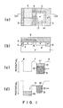
- FIG. 1(a) is a plan view showing the solid-state image pickup device and Fig. 1 (b) is a cross sectional view taken along the lines I b -I b of Fig. 1 (a).
- a p-type semiconductor substrate 1 On the surface of a p-type semiconductor substrate 1, an island-shaped n-type impurity region 2 is formed. By the pn junction of the p-type semiconductor substrate 1 and the n-type impurity region 2, a photoelectric cell is formed.
- a transport channel 16 and an n-type impurity region 4 serving as a charge transfer channel are formed on the surface of the p-type semiconductor substrate.
- the island-shaped n-type impurity region 2 is surrounded by a p-type p + impurity region 3 and is isolated from the adjacent impurity region 2.
- a charge transfer electrode 5 is provided through an insulating layer 6.
- the signal charges 9 and 10 When light is incident on the n-type impurity region 2, signal charges are produced on the pnjunction surface between the p-type semiconductor substrate 1 and the n-type impurity region 2.
- the potential of the charge transfer electrode 5 represents L level
- the signal charges 9 and 10 thus produced are accumulated or stored in the n-type impurity region 2 as shown in Fig. 1 (c).
- the level 8 is a potential level of the p + impurity region 3 for isolation between cells
- the level 7 is a level of the transport channel 16 when the charge transfer electrode 5 is at L level
- the level 11 is a level of the n-type impurity region 2 which has been lowered by the accumulation of the signal charges 9 and 10.
- the level 7 is raised to the level 15 as shown in Fig. 1 (d).
- the signal charge 10 whose level is smaller than the level 15 is transported to the n-type impurity region 4 via the transport channel 16 and is accumulated therein.
- the level of the n-type impurity region 2 is raised to the level 12, so that the signal charge 9 remains therein.
- the n-type impurity region 2 is highly reverse-biased by the potential difference between the level 12 of the n-type impurity region 2 and the level 8 of the n-type impurity region 3 for isolation between cells. Accordingly as signal charges are accumulated, the reverse bias voltage lowers. Accordingly, the width W of the depletion layer formed by the n-type impurity region 2 and the p + impurity region 3 surrounding it becomes narrower as signal charges accumulated increase. As a result, the capacity of the junction of the n-type impurity region 2 and the p + impurity region 3 becomes large.
- the width W of the depletion layer is proportional to one-half power of the reverse bias voltage and depicts a characteristic curve as shown in Fig. 2.
- the impurity concentration of the n-type impurity region 2 is high as is shown in US-A-4 484 210, charges 9 remaining in the n-type impurity region 2 after transportation are increased.
- the well known thermal charge emission occurs to a considerable extent so that charges gradually move to the n-type impurity region 4 serving as the transfer channel, giving rise to afterimage in the solid-state image pickup device.
- the n-type impurity region 2 is formed as is shown in EP-A-0 174 133 so that the impurity concentration thereof is sufficiently lower than that of the p + impurity region 3 serving as the layer for isolation between cells.
- the depletion layer is formed principally within the n-type impurity region 2.
- Reference numerals 13 and 14 in Fig. 1 (a) represent a charge accumulated condition and the edge of the depletion layer within the n-type impurity region 2 immediately after transportation, respectively.
- the width W of the depletion layer becomes broader.
- the junction capacity is lowered, with the result that the charge accumulation capacity becomes small. Accordingly, it is difficult for ensuring a necessary accumulation capacity to lower the impurity concentration of the n-type impurity region 2 to much extent. As a result, there was nothing for it to tolerate that afterimage occurred to some extent.
- An object of the present invention is to provide a solid-state image pickup device in which the charge accumulation capacity is large and the afterimage is little.
- a solid-state image pickup device comprising: a semiconductor substrate of a first conductivity type; a photoelectric cell including an impurity region of a second conductivity type formed on the semiconductor substrate of the first conductivity type to produce a signal charge corresponding to the quantity of an incident light at a first junction surface between the impurity region of the second conductivity type and the semiconductor substrate of the first conductivity type; an impurity region of the first conductivity type formed on the semiconductor substrate of the first conductivity type adjacent to said impurity region of a second conductivity type to effect isolation between the impurity regions of the second conductivity type; and a charge transfer unit for transferring a signal charge produced in the photoelectric device, wherein the impurity concentration of the impurity region of the second conductivity type is high in the vicinity of at least a portion of a second junction surface between the impurity region of the second conductivity type and the impurity region of the first conductivity type, and is low in a range spaced from the second junction surface.
- the solid-state image pickup device Since the solid-state image pickup device according to the present invention is configured as stated above, under a highly reverse-biased condition due to the charge transportation, the portion having high concentration of the impurity region of the second conductivity type is depleted, and under a low reverse-biased condition at the time of charge accumulation, the portion of high concentration is placed in non-depleted condition, whereby the junction capacity at the time of the charge transportation becomes small and the junction capacity at the time of the charge accumulation becomes large to a great extent.
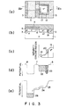
- FIG. 3(a) is a plan view showing the solid-state image pickup device of this embodiment and Fig. 3(b) is a cross sectional view taken along the line IIIb-IIIb of Fig. 3(a).
- Fig. 3(b) is a cross sectional view taken along the line IIIb-IIIb of Fig. 3(a).
- a transport channel 16 and an n-type impurity region 4 serving as a charge transfer channel are formed on the surface of the p-type sem- iconductorsubstrate 1.
- the island-shaped n- impurity region 17 is surrounded by a p + impurity region 3 having high concentration and is isolated from the adjacent n- impurity region 17.
- a charge transfer electrode 5 is provided through an insulating layer 6.
- the solid-state image pickup device of this embodiment is characterized in that there is further provided an n + impurity region 18 having high concentration between the n- impurity region 17 and the p + impurity region 3.
- the n + impurity region 18 having high concentration exists in the vicinity of the junction surface between the n- impurity region 17 and the p + impurity region 3 and surrounds the n- impurity region 17 having low concentration.
- the n + impurity region 18 may completely surround the entire peripheral edge of the n- impurity region 17.
- the impurity concentration distribution of the n- impurity region 17, the n + impurity region 18 and the p + impurity region 3 are shown in Fig. 3(c).
- the n + impurity region 18 As best shown in this figure, with the p + impurity region 3 having high concentration (the concentration distribution 19), the n + impurity region 18 also having high concentration (the concentration distribution 22) is joined. In a range spaced from the junction surface, the n impurity region 17 having low concentration (the concentration distribution 21) exists.
- Fig. 3(d) is the potential diagram in a charge accumulated condition
- Fig. 3(e) is the potential diagram in a charge transfer condition.
- the signal charges 22 and 23 thus produced are accumulated in the n- impurity region 17 and the n + impurity region 18, as shown in Fig. 3(d), respectively.
- the level 8 is a potential level of the p + impurity region 3 for isolation between cells and the level 7 is a level of the transport channel 16 when the charge transfer electrode 5 is at L level.
- the level 7 varies.
- the charges 22 and 23 are moved or transported to the n-type impurity region 4 via the transport channel 16, so that the n- impurity region 17 and n + impurity region are placed in a highly reverse-biased condition.
- a depletion layer extends from the p + impurity region 3 to the n + impurity region 18.
- the voltage of the region 18 reaches a predetermined voltage and is completely depleted, the depletion layer rapidly extends over the n- impurity region 17.
- n- impurity region 17 is in low concentration condition, the expansion of the depletion layerwith respect to the reverse bias voltage increases in proportion to a factor of approximately (N D1 and N D2 are impurity concentrations of the n - impurity region 17 and the n + impurity region 18, respectively). Accordingly, the n - impurity region 17 and the n + impurity region 18 are completely depleted by a small increase of the reverse bias voltage, so that most of remaining charges disappear.
- the potential distribution diagram in this condition is shown in Fig. 3(e), wherein levels 24, 25 and 26 represent potential levels of the n - impurity region 17 and the n + impurity region 18, and a signal charge transported, respectively.
- This model includes a p + impurity region 27 having a high concentration N A , an n + impurity region 28 having a high concentration N D1 and an n - impurity region 29 having a low concentration N D2 wherein it is assumed that these concentrations are uniform in respective regions.
- This model further comprises a voltage source 50 for applying a reverse bias voltage to the p + impurity region 27 and the n + and n - impurity regions 28 and 29.
- the depletion layer extends from the pn junction surface to the p+ impurity region 27 and the n + impurity region 28 as indicated by a hatched region 30 and does not reach the n - impurity region 29.
- N A »N D1 the width W 1 of the depletion layer is expressed as where ⁇ si is a dielectric constant of the silicon semiconductor and e is a quantity of a unit charge. Accordingly, the junction capacity C 1 is expressed as follows:
- the thickness of the n + impurity region 28 is represented with W
- ⁇ T > ⁇ c the n + impurity region 28 is completely depleted, so that it extends to the n - impurity region 29.
- the width of the depletion layerwhich has extended to the n - impurity region 29 is represented with W 2
- the sum of thicknesses W 1 +W 2 can be expressed as follows: where N D1 »N D2 .
- the junction capacity C in this instance is expressed as follows: where ⁇ c can be expressed as
- ⁇ B is a built-in potential
- a curve 34 indicated by the solid line denotes a width of the depletion layer
- a curve 33 indicated by broken lines denotes a junction capacity.
- the junction capacity is large when the relationship of ⁇ T ⁇ c holds in connection with the bias potential difference ⁇ T and abruptly decreases when the bias potential difference ⁇ T sufficiently becomes larger than ⁇ c . Accordingly, under the maximum charge accumulated condition, ⁇ T ⁇ c , and a setting is made such that ⁇ T is sufficiently larger than ⁇ c under the charge transportation condition, thereby making it possible to eliminate afterimage and to increase the maximum charge accumulation capacity.
- FIG. 6(a) is a plan view showing the device in this embodiment and Fig. 6(b) is a cross sectional view taken along the line Vlb-Vlb of Fig. 6(a).
- n + impurity regions 18 are provided in a portion of the junction surface between the n-impurity region 17 and the p + impurity region 3.
- the depletion layer extends from the p + impurity region 3 to the n + impurity region 18 provided in a portion of the junction surface between the n - impurity region 17 and the p + impurity region 3 by the reverse bias thus produced.
- the depletion layer abruptly extends to the n- impurity region 17 in the same manner as in the first embodiment.
- this embodiment can also provide the same advantages as those in the first embodiment.
- FIG. 7(a) is a plan view showing the device in this embodiment and Fig. 7(b) is a cross sectional view taken along the lines VIIIb-VIIb of Fig. 7(a).
- isolation between cells is conducted by using a p- impurity region 39 having low concentration instead of the p + impurity region 3 having high concentration.
- the n + impurity regions 18 are provided in a portion of the junction surface between the n-impurity region 17 and p- impurity region 39 in the same manner as in the second embodiment. Only at portions adjacent to the n + impurity region 18, p + impurity regions 37 are provided. Accordingly, each p + n + junction area between the p + impurity region 37 and the n + impurity region 18 exists in the above-mentioned portion.
- this embodiment can also provide the same advantages as those in the first and second embodiment.
- FIG. 8(a) is a plan view showing the device in this embodiment and Fig. 8(b) is a cross sectional view taken along the lines Vlllb-Vlllb.
- This embodiment is characterized in that an n + impurity region 40 having high concentration is formed so as to overlap with the p + impurity region 3 having high concentration at the upper and lower portion thereof.
- a portion 57 overlapping with the p + impurity region 3 of the n + impurity region 40 serves as an n + impurity region substantially thinner than a portion 58 which does not overlap with the p + impurity region 3 and is depleted at a low voltage. Accordingly, even if the portion 58 is extremely small, the effect can be sufficiently accomplished.
- Fig. 8(c) shows a potential distribution diagram at the time of the charge transportation in this embodiment wherein the potential distribution when charges are transported from the impurity region 57 to the impurity region 58 is indicated by levels 51 and 52.
- the accumulation capacity based on the portion designated at 51 is added without raising a potential required for depletion in addition to the accumulation capacity designated at 52, thus making it possible to conspicuously exhibit the effect of this embodiment. It is needless to say that if the n + impurity region 40 and the p + impurity region 3 overlap in a manner opposite to the above, the effect identical to the above is obtained.
- this embodiment provides the advantage that strict relative positional accuracy with respect to the p + impurity region 3 is not required in the formation of the n + impurity region 40. This is because the n + impurity region 40 has a distribution similar to the distribution shown on Figs. 8(a) and 8(b) even if its concentration distribution deviates toward a concentration range on the side of the p + impurity region 3 or toward a concentration range on the side of the n- impurity region 17.
- FIG. 9(a) is a plan view showing the device in this embodiment and Fig. 9(b) is a cross sectional view taken along the lines IXb-IXb of Fig. 9(a).
- n + impurity regions 40 are provided in a portion of the junction surface between the n - impurity region 17 and the p + impurity regions 3. This embodiment can provide the same advantages as those in the fourth embodiment.
- FIG. 10(a) is a plan view showing the device in this embodiment and Fig. 10(b) is a cross sectional view taken along the lines Xb-Xb of Fig. 10(a).
- isolation between cells or components is implemented by using a p- impurity region 39 having low concentration in place of the p + impurity region 3 having high concentration.
- the n + impurity regions 40 are provided in a portion of the junction surface between the n- impurity region 17 and the p- impurity region 39 in the same manner as in the second embodiment. Only at portions adjacent to the n + impurity regions 40, p + impurity regions 37 are provided. Accordingly, each p + n- junction area between the p + impurity region 37 and the n + impurity region 40 exists in the above-mentioned portion.
- This embodiment can also provide the same advantages as those in the fourth and fifth embodiments.
- the impurity concentration abruptly changes at the boundary between the n-impurity region and the n + impurity region
Landscapes
- Solid State Image Pick-Up Elements (AREA)
- Transforming Light Signals Into Electric Signals (AREA)
Claims (8)
dadurch gekennzeichnet, daß die Verunreinigungskonzentration des Verunreinigungsbereichs des zweiten Leitfähigkeitstyps in der Nähe von wenigstens einem Abschnitt einer zweiten Übergangsoberfläche zwischen dem Verunreinigungsbereich des zweiten Leitfähigkeitstyps und dem Veruneinigungsbereich des ersten Leitfähigkeitstyps hoch ist und in einem von der zweiten Übergangsoberfläche beabstandeten Bereich niedrig ist.
Applications Claiming Priority (2)
| Application Number | Priority Date | Filing Date | Title |
|---|---|---|---|
| JP61163463A JPS6318665A (ja) | 1986-07-11 | 1986-07-11 | 固体撮像装置 |
| JP163463/86 | 1986-07-11 |
Publications (3)
| Publication Number | Publication Date |
|---|---|
| EP0253330A2 EP0253330A2 (de) | 1988-01-20 |
| EP0253330A3 EP0253330A3 (de) | 1991-03-13 |
| EP0253330B1 true EP0253330B1 (de) | 1994-09-28 |
Family
ID=15774352
Family Applications (1)
| Application Number | Title | Priority Date | Filing Date |
|---|---|---|---|
| EP87109999A Expired - Lifetime EP0253330B1 (de) | 1986-07-11 | 1987-07-10 | Festkörperbildaufnahmeanordnung |
Country Status (4)
| Country | Link |
|---|---|
| US (1) | US4907050A (de) |
| EP (1) | EP0253330B1 (de) |
| JP (1) | JPS6318665A (de) |
| DE (1) | DE3750595T2 (de) |
Families Citing this family (14)
| Publication number | Priority date | Publication date | Assignee | Title |
|---|---|---|---|---|
| JPH07112054B2 (ja) * | 1988-03-08 | 1995-11-29 | 株式会社東芝 | 固体撮像装置 |
| JPH0766961B2 (ja) * | 1988-10-07 | 1995-07-19 | 三菱電機株式会社 | 固体撮像素子 |
| JP2575907B2 (ja) * | 1989-12-28 | 1997-01-29 | 株式会社東芝 | 固体撮像装置とその製造方法 |
| US5130774A (en) * | 1990-07-12 | 1992-07-14 | Eastman Kodak Company | Antiblooming structure for solid-state image sensor |
| JPH0828497B2 (ja) * | 1990-07-19 | 1996-03-21 | 株式会社東芝 | 固体撮像装置 |
| US5291044A (en) * | 1990-12-12 | 1994-03-01 | Eastman Kodak Company | Image sensor with continuous time photodiode |
| JP2849249B2 (ja) * | 1991-10-22 | 1999-01-20 | 三菱電機株式会社 | 赤外イメージセンサ及びその製造方法 |
| EP0544260A1 (de) * | 1991-11-25 | 1993-06-02 | Eastman Kodak Company | Überlaufvorrichtung für einen CCD-Bildsensor |
| US5705836A (en) * | 1995-05-22 | 1998-01-06 | Dalsa, Inc. | Efficient charge transfer structure in large pitch charge coupled device |
| US6346722B1 (en) | 1998-06-26 | 2002-02-12 | Nec Corporation | Solid state imaging device and method for manufacturing the same |
| US6310366B1 (en) * | 1999-06-16 | 2001-10-30 | Micron Technology, Inc. | Retrograde well structure for a CMOS imager |
| JP2005302909A (ja) * | 2004-04-09 | 2005-10-27 | Sony Corp | 固体撮像素子及びその製造方法 |
| JP2017045879A (ja) * | 2015-08-27 | 2017-03-02 | 株式会社東芝 | 固体撮像装置および固体撮像装置の製造方法 |
| JP2019114797A (ja) * | 2019-02-20 | 2019-07-11 | 株式会社東芝 | 固体撮像装置および固体撮像装置の製造方法 |
Family Cites Families (4)
| Publication number | Priority date | Publication date | Assignee | Title |
|---|---|---|---|---|
| US4484210A (en) * | 1980-09-05 | 1984-11-20 | Nippon Electric Co., Ltd. | Solid-state imaging device having a reduced image lag |
| JPS5887882A (ja) * | 1981-11-20 | 1983-05-25 | Hitachi Ltd | フオトセンサ− |
| JPS5928772A (ja) * | 1982-08-11 | 1984-02-15 | Sony Corp | 固体撮像装置の駆動方法 |
| JPS6156583A (ja) * | 1984-08-27 | 1986-03-22 | Sharp Corp | 固体撮像装置 |
-
1986
- 1986-07-11 JP JP61163463A patent/JPS6318665A/ja active Granted
-
1987
- 1987-07-09 US US07/071,665 patent/US4907050A/en not_active Expired - Lifetime
- 1987-07-10 EP EP87109999A patent/EP0253330B1/de not_active Expired - Lifetime
- 1987-07-10 DE DE3750595T patent/DE3750595T2/de not_active Expired - Fee Related
Also Published As
| Publication number | Publication date |
|---|---|
| EP0253330A3 (de) | 1991-03-13 |
| JPH0516669B2 (de) | 1993-03-05 |
| US4907050A (en) | 1990-03-06 |
| JPS6318665A (ja) | 1988-01-26 |
| EP0253330A2 (de) | 1988-01-20 |
| DE3750595D1 (de) | 1994-11-03 |
| DE3750595T2 (de) | 1995-03-23 |
Similar Documents
| Publication | Publication Date | Title |
|---|---|---|
| US6649951B2 (en) | Light-receiving element and photoelectric conversion device | |
| EP1636856B1 (de) | Ultradünne, rückbeleuchtete fotodioden-array-strukturen und herstellungsverfahren | |
| US4733286A (en) | Semiconductor photoelectric converting device | |
| EP0253330A2 (de) | Festkörperbildaufnahmeanordnung | |
| US5130774A (en) | Antiblooming structure for solid-state image sensor | |
| JPH06500431A (ja) | フォトダイオードとccdエレメントとの間に転送ゲートを有するイメージセンサ | |
| EP0908956B1 (de) | Photoelektrische Umwandlungsvorrichtung und Bildsensor | |
| US5181093A (en) | Solid state image sensor having high charge transfer efficiency | |
| EP0069535A2 (de) | Festkörperbildaufnahmegerät | |
| EP0174133B1 (de) | Festkörper-Bildsensor | |
| JPS6065565A (ja) | 固体撮像素子 | |
| EP0132870B1 (de) | Strahlungsempfindliche Halbleitervorrichtung | |
| JPH114012A (ja) | Pinフォトダイオード | |
| JP2521789B2 (ja) | 固体撮像装置の感光部構造 | |
| JPH04502234A (ja) | 固体撮像器 | |
| JPS6170874A (ja) | 固体撮像素子 | |
| JPH0135546B2 (de) | ||
| JPS6134263B2 (de) | ||
| EP4369421A1 (de) | Lichtempfangsvorrichtung, röntgenbildgebungsvorrichtung und elektronische ausrüstung | |
| EP0037200A1 (de) | Ladungsgekoppelte Vorrichtung mit vergrabener Kanalbegrenzungszone | |
| JPS62155559A (ja) | 固体撮像装置 | |
| JPS59196667A (ja) | 固体撮像装置 | |
| GB2248341A (en) | Infra-red radiation imaging device arrangements | |
| JPS58125975A (ja) | 固体撮像素子 | |
| JPS6251254A (ja) | 固体撮像装置 |
Legal Events
| Date | Code | Title | Description |
|---|---|---|---|
| PUAI | Public reference made under article 153(3) epc to a published international application that has entered the european phase |
Free format text: ORIGINAL CODE: 0009012 |
|
| 17P | Request for examination filed |
Effective date: 19870710 |
|
| AK | Designated contracting states |
Kind code of ref document: A2 Designated state(s): DE FR GB |
|
| PUAL | Search report despatched |
Free format text: ORIGINAL CODE: 0009013 |
|
| AK | Designated contracting states |
Kind code of ref document: A3 Designated state(s): DE FR GB |
|
| 17Q | First examination report despatched |
Effective date: 19920625 |
|
| GRAA | (expected) grant |
Free format text: ORIGINAL CODE: 0009210 |
|
| AK | Designated contracting states |
Kind code of ref document: B1 Designated state(s): DE FR GB |
|
| REF | Corresponds to: |
Ref document number: 3750595 Country of ref document: DE Date of ref document: 19941103 |
|
| ET | Fr: translation filed | ||
| PLBE | No opposition filed within time limit |
Free format text: ORIGINAL CODE: 0009261 |
|
| STAA | Information on the status of an ep patent application or granted ep patent |
Free format text: STATUS: NO OPPOSITION FILED WITHIN TIME LIMIT |
|
| 26N | No opposition filed | ||
| PGFP | Annual fee paid to national office [announced via postgrant information from national office to epo] |
Ref country code: GB Payment date: 19970701 Year of fee payment: 11 |
|
| PGFP | Annual fee paid to national office [announced via postgrant information from national office to epo] |
Ref country code: FR Payment date: 19970709 Year of fee payment: 11 |
|
| PG25 | Lapsed in a contracting state [announced via postgrant information from national office to epo] |
Ref country code: GB Free format text: LAPSE BECAUSE OF NON-PAYMENT OF DUE FEES Effective date: 19980710 |
|
| GBPC | Gb: european patent ceased through non-payment of renewal fee |
Effective date: 19980710 |
|
| PG25 | Lapsed in a contracting state [announced via postgrant information from national office to epo] |
Ref country code: FR Free format text: LAPSE BECAUSE OF NON-PAYMENT OF DUE FEES Effective date: 19990331 |
|
| REG | Reference to a national code |
Ref country code: FR Ref legal event code: ST |
|
| PGFP | Annual fee paid to national office [announced via postgrant information from national office to epo] |
Ref country code: DE Payment date: 20050707 Year of fee payment: 19 |
|
| PG25 | Lapsed in a contracting state [announced via postgrant information from national office to epo] |
Ref country code: DE Free format text: LAPSE BECAUSE OF NON-PAYMENT OF DUE FEES Effective date: 20070201 |