EP0253352B1 - Système de traitement de données graphiques - Google Patents
Système de traitement de données graphiques Download PDFInfo
- Publication number
- EP0253352B1 EP0253352B1 EP87110099A EP87110099A EP0253352B1 EP 0253352 B1 EP0253352 B1 EP 0253352B1 EP 87110099 A EP87110099 A EP 87110099A EP 87110099 A EP87110099 A EP 87110099A EP 0253352 B1 EP0253352 B1 EP 0253352B1
- Authority
- EP
- European Patent Office
- Prior art keywords
- data
- pixel
- processing system
- image memory
- graphic data
- Prior art date
- Legal status (The legal status is an assumption and is not a legal conclusion. Google has not performed a legal analysis and makes no representation as to the accuracy of the status listed.)
- Expired - Lifetime
Links
Images




Classifications
-
- G—PHYSICS
- G09—EDUCATION; CRYPTOGRAPHY; DISPLAY; ADVERTISING; SEALS
- G09G—ARRANGEMENTS OR CIRCUITS FOR CONTROL OF INDICATING DEVICES USING STATIC MEANS TO PRESENT VARIABLE INFORMATION
- G09G5/00—Control arrangements or circuits for visual indicators common to cathode-ray tube indicators and other visual indicators
- G09G5/02—Control arrangements or circuits for visual indicators common to cathode-ray tube indicators and other visual indicators characterised by the way in which colour is displayed
- G09G5/024—Control arrangements or circuits for visual indicators common to cathode-ray tube indicators and other visual indicators characterised by the way in which colour is displayed using colour registers, e.g. to control background, foreground, surface filling
-
- G—PHYSICS
- G09—EDUCATION; CRYPTOGRAPHY; DISPLAY; ADVERTISING; SEALS
- G09G—ARRANGEMENTS OR CIRCUITS FOR CONTROL OF INDICATING DEVICES USING STATIC MEANS TO PRESENT VARIABLE INFORMATION
- G09G5/00—Control arrangements or circuits for visual indicators common to cathode-ray tube indicators and other visual indicators
- G09G5/02—Control arrangements or circuits for visual indicators common to cathode-ray tube indicators and other visual indicators characterised by the way in which colour is displayed
Definitions
- the present invention relates to a graphic data processing system and, more particularly, to a graphic data processing system which is appropriate for increasing the processing rate.
- a system of the prior art is constructed as follows, as is disclosed in EP-A- 0146961 (July 3, 1985): Pixel addresses composed of address informations for designating addresses of an image memory and pixel position designating informations for designating pixel positions in one word, which are designated by the addresses, are sequentially calculated. The one-word graphic data designated by the address informations of the pixel addresses calculated are read out from the image memory. Then, with informations decoded from the pixel position designating informations of the pixel addresses for designating a plurality of bit positions corresponding to the designated pixel positions, only a predetermined bit expressing one pixel of the graphic data read out is subjected to a graphic logical operation. The result of this logical operation is written again in the image memory so that it may be displayed.
- the one-word graphic data in the image memory are considered such that the processing performance may be equivalent to that for a monochromatic image irrespective of the bit number composing one pixel.
- the one-word graphic data in the image memory have informations of plural pixels, no consideration is taken into the point that those plural pixels are processed simultaneously in parallel.
- the graphic data in the same address of the image memory have to be accessed and processed a plurality of times, thus raising a problem that the processing rate is decreased.
- EP-A-0 071 744 describes a method for operating a computing system to write text characters onto a graphics display.
- a processor writes a character to a display by selecting and loading into a graphics video display buffer a text character dot pattern retrieved from the main storage, and expanded to a selected pixel and color format, and reads a character previously written by comparing a dot pattern retrieved from the display buffer with dot patterns retrieved from the main storage.
- An object of the present invention is to provide a graphic data processing system which can draw an image at a processing rate as high as that in the case in which one word of an image memory has a single pixel, even in case the one word has a plurality of pixels.
- the data extending means extends the data in the image memory into one word simultaneously, and the multiplexer multiplexes the color information independently at each bit on the basis of the extended data.
- the graphic data processing system according to the present invention processes the plural pixels in one word simultaneously in parallel.
- FIG. 2 is a block diagram showing a graphic data processing system according to the embodiment of the present invention.
- a processor 10 which may preferably be formed on a single semiconductor substrate, is connected on one hand with a central processing unit (i.e., CPU) 11, which may preferably be formed on the other single semiconductor substrate, and on the other with an image memory 12 formed of a font data region and a display region.
- This image memory 12 is connected through a display conversion device 13 with either a image output device 14 such as a cRT, a liquid crystal display or an EL display or an image output device 14 represented by a printer or the like.
- the processor 10 is constructed of an arithmetic device 100 for reading, rewriting and writing the data of the image memory 12, and a control device 110 for controlling the arithmetic device 100 in a constant sequence.
- the arithmetic device 100 is further divided into a logical addressing unit 120, a physical addressing unit 130 and a color data arithmetic unit 140.
- the data stored in the font region of the image memory 12 are arithmetically processed by the arithmetic device 100 of the processor 10. More specifically, where a drawing point is in the display frame is logically and arithmetically calculated in the logical addressing unit 120 mainly in accordance with a drawing algorithm.
- the actual physical address of the image memory 12 is made in the physical addressing unit 130.
- the color data to be written in the image memory 12 are calculated in the color data arithmetic unit 140.
- the result calculated by the arithmetic device 100 is sent to the display region of the image memory 12 in accordance with the instruction of the central processing unit (CPU) 11.
- the data of the image memory 12 are converted by the display conversion device 13 into display data, which are sent to the display device 14.
- Fig. 3 presents diagrams showing the bit structures of one word in individual pixel modes of the image memory 12
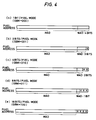
- Fig. 4 presents diagrams showing pixel addresses corresponding to the pixel modes, respectively
- Fig. 5 is a diagram showing the spacial arrangement of the image memory 12.
- This mode expresses one pixel with two bits and is used to display four colors or tones at the maximum. Data of a series of eight pixels are stored in one word of the image memory 12. Moreover, the GBM signal is "001".
- This mode expresses one pixel with four bits, and data of a series of four pixels are stored in one word of the image memory 12. Moreover, the GBM signal is "010".
- This mode expresses one pixel with eight bits, and data of two pixels are stored in one word of the image memory 12. Moreover, the GBM signal is "011".
- This mode expresses one pixel with sixteen bits, and one word of the pixel memory 12 corresponds to one-pixel data. Moreover, the GBM signal is "100".
- a pixel address is adopted.
- This pixel address is constructed, as shown in Fig. 4, of address information MAD for designating the address of the image memory 12, and pixel position designating information WAD for designating what the position is in one word designated with the address.
- the pixel position designating information WAD is prepared as a bit address, i.e., a part of a physical address in the less significant four bits of the pixel address and is calculated by the physical addressing unit 130.
- the pixel position designating information WAD at the less significant four bits is used to designate the pixel position in one word in accordance with each bit / pixel mode.
- symbols "*" appearing in Fig. 4 indicate bits having no relation to the arithmetic.
- the image data in one word at the address of the image memory 12 designated with the address information MAD in the pixel address are read out all at once from the image memory 12. Then, only a predetermined bit part of the image data is modified on the basis of the pixel position designating information in the pixel address, the GBM signal indicating the bit number composing one pixel, and the information indicating the number of pixels to be updated.
- the image data thus modified are written in the corresponding address of the image memory 12.
- a plurality of bits corresponding to one or plural pixels are processed simultaneously in parallel.
- the spacial arrangement of the image memory 12 in case the pixel mode is the four bits / pixel mode is shown in Fig. 5.
- the address of the image memory 12 is assigned as a linear address, as shown in a memory map (A) of Fig. 5, and is displayed as a two-dimensional image, as shown at (B) in Fig. 5.
- the Memory Width MW of the display frame indicates how many bits the horizontal width of the display frame is composed of. In the case of the four bits / pixel mode, therefore, a MW/4 pixel is displayed in the horizontal direction. Since one pixel is displayed with four bits, moreover, one-word data are displayed as data of a series of four pixels in the horizontal direction, as shown at (C) in Fig. 5.
- the number of the bits composing one pixel may be added or subtracted so as to shift the physical address one pixel in the horizontal direction, whereas the value of MW may be added or subtracted so as to move the same one pixel in the vertical direction.
- the bit number of one word may be added or subtracted so as to process the plural pixels of one word.
- Figs. 1 and 6 are block diagrams showing the major portions of the graphic data processing system according to the present invention, respectively.
- the font data region of the image memory 12 is connected with the input of the color data arithmetic unit 140 of the image memory 12, and the output of this color data arithmetic unit 140 is connected with the display region of the image memory 12.
- the color data arithmetic unit 140 is constructed of a font data register (FDR) 1401, a data extending circuit 1402, a source latch (SLSFT) 1403, a barrel shifter (BARREL SFT) 1404, a destination latch 1 (DLC1) 1405, a destination latch 2 (DLC1) 1406, a color register 0 (CL0) 1407, a color register 1 (CL1) 1408, a multiplexer (MPX) 1409, a graphic mask register (G MASK) 1410, a drawing mode register (DM) 1411, a color data comparator (CLCMP) 1412, a coincidence detecting circuit 1413, a condition judging circuit 1414, a signal extending circuit 1415, a logical arithmetic unit (LU) 1416, a write data buffer (WDBR) 1417, a read data buffer (RDBR) 1418, and a memory address register (MAR) 1419.
- FDR font data register
- DLC1 destination latch 1
- DLC1 destination latch 2
- the font data thus inputted are first read in the read data buffer (RDBR) 1418 of the color data arithmetic unit 140 and then latched in the font data register (FDR) 1401.
- the font data thus latched are extended (simultaneously by one word) by the data extending circuit 1402 in response to the GBM signal indicating the bit number composing one pixel.
- SL SFT source latch
- These extended data are shifted by the barrel shifter (BARREL SFT) 1404 to a bit position indicated by a written pixel address so that their bits may be arranged with those of the written data.
- This shifted result is temporarily stored in the (M) of the destination latch 1 (DLCl) 1405, and the (M) data are composed with the previous shift result (the (S) of the destination latch 1) to generate information corresponding to the write data.
- the font data are judged for each bit whether the signal is at "0" or "1".
- the values of color data 0 and 1 are selected for the "0" and “1" signals, respectively.
- Color data 0 and 1 are latched in the color registers 0 (CL0) 1407 and the color register 1 (CL1) 1408, respectively.
- the data composed in the destination latch 1 (DLC1) 1405 are used as multiplex signals for selecting the color data 0 and 1 which are latched in those color register 0 (CL0) 1407 and color register 1 (CL1) 1408, respectively. As shown in Fig.
- the multiplexer 1409 for selecting one bit is used for one word to select the color data 0 and 1, which are latched in the color register 0 (CL0) 1407 and the color register 1 (CL1) 1408, respectively, and the data of the destination latch (DLC1) 1405 independently for each bit, thus producing the write data.
- write data are sent to the logical arithmetic unit (LU) 1416 so that their logical arithmetic with the written data may be performed.
- This logical arithmetic unit (LU) 1416 is enabled to select the kind of the logical arithmetic operations in accordance with the mode designated by the drawing mode register (DM) 1411 and to designate a no-operation at each bit. In this no-operation case, the written data are outputted as they are. As a result, the case in which one word has bits left unwritten can be coped with by designating that bit with a no-operation signal.
- This no-operation signal is set in the graphic mask register (G MASK) 1410 by the control device 110 on the basis of the GBM signal and the information of the number of pixels to be processed.
- the output of the logical arithmetic unit (LU) 1416 are set in the write data buffer (WDBR) 1417 and written in the display region of the image memory 12.
- the no-operation signal is connected with the output signal of a color condition comparator which is constructed of the color data comparator (CLCMP) 1412, the coincidence detecting circuit 1413, the condition judging circuit 1414 and the signal extending circuit 1415.
- CLCMP color data comparator
- the magnitudes of the write data and the written data are judged for one word at the unit of pixel.
- Each bit of the pixel having failed to match the condition designated by the drawing mode register (DM) 1411 is used as the no-operation signal.
- the drawing can be accomplished without deteriorating the background color of the character.
- the relation between the color condition comparator and the logical arithmetic unit (LU) 1416 is such that the color data comparator (CLCMP) 1412 of the color condition comparator makes a judgement of the magnitudes at the unit of each pixel while deemping the bits in one pixel as a binary code, as shown in Fig. 9.
- the color data comparator (CLCMP) 1412 outputs the bits of the "1" signal, if the condition is satisfied, and otherwise the bits of the "0" signal.
- the logical arithmetic unit (LU) 1416 performs a logical arithmetic operation of only the portion of the "1" signal of that judged output bit and transfers the result to the write destination.
- the data thus transferred to the display region of the image memory 12 are converted into a multi-bit value, e.g., four bits / pixel, as shown in Fig. 1, although the font data stored in the font data region of the image memory 12 are monochromatic.
- data of a plurality of pixels can be processed all at once by one reading, updating and writing process so that a drawing can be accomplished in a high memory accessing efficiency. Since, moreover, the font extension can be controlled in accordance with the bit length of one pixel, the structure can have a wide use.
- the drawing process can be speeded up because the data of a plurality of pixels in one word can be changed by the single reading, updating and writing process.
Landscapes
- Engineering & Computer Science (AREA)
- Physics & Mathematics (AREA)
- Computer Hardware Design (AREA)
- General Physics & Mathematics (AREA)
- Theoretical Computer Science (AREA)
- Controls And Circuits For Display Device (AREA)
Claims (6)
- Système de traitement de données graphiques comprenant :
une mémoire d'images (12) pour mémoriser un motif de caractère sous la forme de données de police constituées par au moins une information monochrome, et pour mémoriser les données graphiques du motif de caractère;
des premier et second registres de couleurs (1407, 1408) pour conserver une information correspondant respectivement aux valeurs "0" et "1" des données de police mémorisées dans ladite mémoire d'images (12); et
des moyens (1410) pour masquer et enregistrer des données qui sont sélectionnées en tant que données graphiques;
caractérisé en ce que
des moyens d'extension de données (1402) sont prévus pour étendre simultanément m bits de données de police présentant m pixels, mémorisés dans ladite mémoire d'images (12), en m x n bits de données de police, n étant le nombre de bits représentant un pixel; et
un multiplexeur (1409) est prévu pour la sélection des données de couleurs à partir desdits registres de couleurs (1407, 1408), des valeurs "0" et "1" des données étendues étant utilisées pour produire des signaux de commande pour ledit multiplexeur (1409). - Système de traitement graphique selon la revendication 1, comprenant en outre des moyens pour désigner à volonté le nombre n de bits.
- Système de traitement de données graphiques selon la revendication 1, dans lequel ledit motif de police est formé avec (k x 1) profils de bits binaires.
- Système de traitement de données graphiques selon la revendication 1, dans lequel un dispositif de délivrance d'images est prévu pour délivrer des données d'images enregistrées dans ladite mémoire d'images (12).
- Système de traitement de données graphiques selon la revendication 4, dans lequel ledit dispositif de délivrance d'images est un dispositif d'affichage.
- Système de traitement de données graphiques selon la revendication 4, dans lequel ledit dispositif de délivrance d'images est une imprimante.
Applications Claiming Priority (2)
| Application Number | Priority Date | Filing Date | Title |
|---|---|---|---|
| JP61165393A JP2835719B2 (ja) | 1986-07-14 | 1986-07-14 | 画像処理装置 |
| JP165393/86 | 1986-07-14 |
Publications (3)
| Publication Number | Publication Date |
|---|---|
| EP0253352A2 EP0253352A2 (fr) | 1988-01-20 |
| EP0253352A3 EP0253352A3 (en) | 1990-09-12 |
| EP0253352B1 true EP0253352B1 (fr) | 1994-10-05 |
Family
ID=15811546
Family Applications (1)
| Application Number | Title | Priority Date | Filing Date |
|---|---|---|---|
| EP87110099A Expired - Lifetime EP0253352B1 (fr) | 1986-07-14 | 1987-07-13 | Système de traitement de données graphiques |
Country Status (5)
| Country | Link |
|---|---|
| US (1) | US5159320A (fr) |
| EP (1) | EP0253352B1 (fr) |
| JP (1) | JP2835719B2 (fr) |
| KR (1) | KR970004538B1 (fr) |
| DE (1) | DE3750622T2 (fr) |
Families Citing this family (9)
| Publication number | Priority date | Publication date | Assignee | Title |
|---|---|---|---|---|
| EP0422294A1 (fr) * | 1989-10-12 | 1991-04-17 | International Business Machines Corporation | Système d'affichage |
| JP2704954B2 (ja) * | 1991-06-21 | 1998-01-26 | 富士通株式会社 | ビット拡張装置 |
| US6351263B1 (en) * | 1992-07-28 | 2002-02-26 | Canon Kabushiki Kaisha | Image processor which manually and independently designates processing parameters for character data and image data |
| CA2131414A1 (fr) * | 1993-09-22 | 1995-03-23 | Michael Abrash | Production rapide de donnees en 256 couleurs a l'aide d'un adaptateur vga |
| GB9513515D0 (en) * | 1995-07-03 | 1995-09-06 | Sgs Thomson Microelectronics | Expansion of data |
| US5764963A (en) * | 1995-07-07 | 1998-06-09 | Rambus, Inc. | Method and apparatus for performing maskable multiple color block writes |
| US6762770B1 (en) * | 1999-10-29 | 2004-07-13 | Apple Computer, Inc. | Method and system for the representation of color and other attributes in bitmap fonts |
| JP3816882B2 (ja) * | 2003-03-05 | 2006-08-30 | 株式会社東芝 | 表示用フォントメモリ |
| US11755336B2 (en) * | 2021-09-29 | 2023-09-12 | Advanced Micro Devices, Inc. | Distributed geometry |
Family Cites Families (13)
| Publication number | Priority date | Publication date | Assignee | Title |
|---|---|---|---|---|
| US3573789A (en) * | 1968-12-13 | 1971-04-06 | Ibm | Method and apparatus for increasing image resolution |
| US3911418A (en) * | 1969-10-08 | 1975-10-07 | Matsushita Electric Industrial Co Ltd | Method and apparatus for independent color control of alphanumeric display and background therefor |
| US3893100A (en) * | 1973-12-20 | 1975-07-01 | Data Royal Inc | Variable size character generator with constant display density method |
| US4408200A (en) * | 1981-08-12 | 1983-10-04 | International Business Machines Corporation | Apparatus and method for reading and writing text characters in a graphics display |
| US4467322A (en) * | 1982-08-30 | 1984-08-21 | Sperry Corporation | Digital shade control for color CRT background and cursors |
| US4639721A (en) * | 1982-10-09 | 1987-01-27 | Sharp Kabushiki Kaisha | Data selection circuit for the screen display of data from a personal computer |
| US4555802A (en) * | 1983-01-10 | 1985-11-26 | International Business Machines Corporation | Compaction and decompaction of non-coded information bearing signals |
| US4591842A (en) * | 1983-05-26 | 1986-05-27 | Honeywell Inc. | Apparatus for controlling the background and foreground colors displayed by raster graphic system |
| DE3474933D1 (en) * | 1983-07-26 | 1988-12-08 | Oki Electric Ind Co Ltd | Printing system for a dot printer |
| JPH06100911B2 (ja) * | 1983-12-26 | 1994-12-12 | 株式会社日立製作所 | 画像データ処理装置及び方法 |
| DE3486472T2 (de) * | 1983-12-26 | 1999-11-25 | Hitachi Eng Co Ltd | Graphisches Musterverarbeitungsgerät und Verfahren |
| JPS60165696A (ja) * | 1984-02-08 | 1985-08-28 | 株式会社アスキ− | デイスプレイコントロ−ラ |
| JPS6117189A (ja) * | 1985-04-19 | 1986-01-25 | 株式会社日立製作所 | 図形処理装置 |
-
1986
- 1986-07-14 JP JP61165393A patent/JP2835719B2/ja not_active Expired - Lifetime
-
1987
- 1987-07-13 DE DE3750622T patent/DE3750622T2/de not_active Expired - Fee Related
- 1987-07-13 EP EP87110099A patent/EP0253352B1/fr not_active Expired - Lifetime
- 1987-07-14 KR KR1019870007583A patent/KR970004538B1/ko not_active Expired - Fee Related
-
1990
- 1990-08-10 US US07/565,910 patent/US5159320A/en not_active Expired - Lifetime
Also Published As
| Publication number | Publication date |
|---|---|
| EP0253352A2 (fr) | 1988-01-20 |
| US5159320A (en) | 1992-10-27 |
| JPS6321694A (ja) | 1988-01-29 |
| DE3750622D1 (de) | 1994-11-10 |
| KR880002094A (ko) | 1988-04-29 |
| EP0253352A3 (en) | 1990-09-12 |
| DE3750622T2 (de) | 1995-02-16 |
| JP2835719B2 (ja) | 1998-12-14 |
| KR970004538B1 (ko) | 1997-03-28 |
Similar Documents
| Publication | Publication Date | Title |
|---|---|---|
| US4278973A (en) | Video display terminal with partitioned screen | |
| US4718024A (en) | Graphics data processing apparatus for graphic image operations upon data of independently selectable pitch | |
| US5056041A (en) | Data processing apparatus with improved bit masking capability | |
| US20010052903A1 (en) | Graphic pattern processing apparatus | |
| US4984183A (en) | Graphics display controller for transferring figure data to overlapping portions of destination area and drawing-enable area defined by clipping rectangle | |
| US5923340A (en) | Process of processing graphics data | |
| US5596767A (en) | Programmable data processing system and apparatus for executing both general purpose instructions and special purpose graphic instructions | |
| US5185859A (en) | Graphics processor, a graphics computer system, and a process of masking selected bits | |
| US5159320A (en) | Graphic data processing system for extending font data into color data which is input into an image memory | |
| US5313227A (en) | Graphic display system capable of cutting out partial images | |
| US6005537A (en) | Liquid-crystal display control apparatus | |
| US5333261A (en) | Graphics processing apparatus having instruction which operates separately on X and Y coordinates of pixel location registers | |
| US5375198A (en) | Process for performing a windowing operation in an array move, a graphics computer system, a display system, a graphic processor and a graphics display system | |
| EP0256838B1 (fr) | Système pour améliorer le fonctionnement des affichages à deux couleurs | |
| JPH0562348B2 (fr) | ||
| JPH06100911B2 (ja) | 画像データ処理装置及び方法 | |
| US5157766A (en) | Boundary drawing and area filling logic for a display system | |
| KR960003072B1 (ko) | 폰트 데이타 처리장치 | |
| EP0466935B1 (fr) | Dispositif d'affichage d'images immobiles et cartouche de memoire externe utilisee avec un tel dispositif | |
| US4941110A (en) | Memory saving arrangement for displaying raster test patterns | |
| JP2656754B2 (ja) | 画像データ処理装置及びそれを用いたシステム | |
| JP2824744B2 (ja) | 画像処理装置、データ処理装置およびデータ処理システム | |
| JPH07109549B2 (ja) | グラフィックプロセッサ | |
| JPS63304293A (ja) | 表示メモリ制御回路 | |
| JPH0786915B2 (ja) | 画像処理装置 |
Legal Events
| Date | Code | Title | Description |
|---|---|---|---|
| PUAI | Public reference made under article 153(3) epc to a published international application that has entered the european phase |
Free format text: ORIGINAL CODE: 0009012 |
|
| AK | Designated contracting states |
Kind code of ref document: A2 Designated state(s): DE FR GB IT |
|
| PUAL | Search report despatched |
Free format text: ORIGINAL CODE: 0009013 |
|
| AK | Designated contracting states |
Kind code of ref document: A3 Designated state(s): DE FR GB IT |
|
| 17P | Request for examination filed |
Effective date: 19900920 |
|
| 17Q | First examination report despatched |
Effective date: 19920630 |
|
| GRAA | (expected) grant |
Free format text: ORIGINAL CODE: 0009210 |
|
| AK | Designated contracting states |
Kind code of ref document: B1 Designated state(s): DE FR GB IT |
|
| REF | Corresponds to: |
Ref document number: 3750622 Country of ref document: DE Date of ref document: 19941110 |
|
| ITF | It: translation for a ep patent filed | ||
| ET | Fr: translation filed | ||
| PLBE | No opposition filed within time limit |
Free format text: ORIGINAL CODE: 0009261 |
|
| 26N | No opposition filed | ||
| PGFP | Annual fee paid to national office [announced via postgrant information from national office to epo] |
Ref country code: FR Payment date: 20010625 Year of fee payment: 15 |
|
| PGFP | Annual fee paid to national office [announced via postgrant information from national office to epo] |
Ref country code: GB Payment date: 20010628 Year of fee payment: 15 |
|
| PGFP | Annual fee paid to national office [announced via postgrant information from national office to epo] |
Ref country code: DE Payment date: 20010928 Year of fee payment: 15 |
|
| REG | Reference to a national code |
Ref country code: GB Ref legal event code: IF02 |
|
| PG25 | Lapsed in a contracting state [announced via postgrant information from national office to epo] |
Ref country code: GB Free format text: LAPSE BECAUSE OF NON-PAYMENT OF DUE FEES Effective date: 20020713 |
|
| PG25 | Lapsed in a contracting state [announced via postgrant information from national office to epo] |
Ref country code: DE Free format text: LAPSE BECAUSE OF NON-PAYMENT OF DUE FEES Effective date: 20030201 |
|
| GBPC | Gb: european patent ceased through non-payment of renewal fee |
Effective date: 20020713 |
|
| PG25 | Lapsed in a contracting state [announced via postgrant information from national office to epo] |
Ref country code: FR Free format text: LAPSE BECAUSE OF NON-PAYMENT OF DUE FEES Effective date: 20030331 |
|
| REG | Reference to a national code |
Ref country code: FR Ref legal event code: ST |
|
| PG25 | Lapsed in a contracting state [announced via postgrant information from national office to epo] |
Ref country code: IT Free format text: LAPSE BECAUSE OF NON-PAYMENT OF DUE FEES;WARNING: LAPSES OF ITALIAN PATENTS WITH EFFECTIVE DATE BEFORE 2007 MAY HAVE OCCURRED AT ANY TIME BEFORE 2007. THE CORRECT EFFECTIVE DATE MAY BE DIFFERENT FROM THE ONE RECORDED. Effective date: 20050713 |