EP0254071A2 - Dispositif transistor à couche mince amorphe - Google Patents
Dispositif transistor à couche mince amorphe Download PDFInfo
- Publication number
- EP0254071A2 EP0254071A2 EP87109211A EP87109211A EP0254071A2 EP 0254071 A2 EP0254071 A2 EP 0254071A2 EP 87109211 A EP87109211 A EP 87109211A EP 87109211 A EP87109211 A EP 87109211A EP 0254071 A2 EP0254071 A2 EP 0254071A2
- Authority
- EP
- European Patent Office
- Prior art keywords
- gate
- electrode
- semiconductor
- layer
- parallel
- Prior art date
- Legal status (The legal status is an assumption and is not a legal conclusion. Google has not performed a legal analysis and makes no representation as to the accuracy of the status listed.)
- Granted
Links
Images


Classifications
-
- H—ELECTRICITY
- H10—SEMICONDUCTOR DEVICES; ELECTRIC SOLID-STATE DEVICES NOT OTHERWISE PROVIDED FOR
- H10D—INORGANIC ELECTRIC SEMICONDUCTOR DEVICES
- H10D30/00—Field-effect transistors [FET]
- H10D30/60—Insulated-gate field-effect transistors [IGFET]
- H10D30/67—Thin-film transistors [TFT]
- H10D30/6728—Vertical TFTs
-
- H—ELECTRICITY
- H10—SEMICONDUCTOR DEVICES; ELECTRIC SOLID-STATE DEVICES NOT OTHERWISE PROVIDED FOR
- H10W—GENERIC PACKAGES, INTERCONNECTIONS, CONNECTORS OR OTHER CONSTRUCTIONAL DETAILS OF DEVICES COVERED BY CLASS H10
- H10W20/00—Interconnections in chips, wafers or substrates
- H10W20/40—Interconnections external to wafers or substrates, e.g. back-end-of-line [BEOL] metallisations or vias connecting to gate electrodes
Definitions
- the field of the invention is in transistors where the semiconductor member is an amorphous layer usually of hydrogenated or fluorinated silicon although crystalline films of silicon or group II-VI compound semiconductors are currently receiving study. Such devices have come to be known in the art as thin film transistors.
- Thin film transistor devices have the advantages of economy and compatibility with large area deposition type fabrication technology.
- the thin film transistor has a structure similar to a conventional field effect transistor in that there are source and drain ohmic electrodes separated by a channel and conduction in the channel, which in the thin film transistor is amorphous, is under the control of a signal applied through a gate electrode in electric field influencing proximity to the channel.
- the general technology of thin film transistors has been to provide an array of gate metal elements on a substrate and then to cover the gates first with an insulation layer and then with amorphous silicon up and over each gate metal element and positioning source and drain electrodes on top of the amorphous silicon.
- the invention is thin film transistor technology where a gate electrode in the shape of a prism with essentially vertical sides is positioned on a substrate and covered by a series of layers at least one of which, adjacent to the semiconductor layer, is applied from a direction orthogonal to the substrate surface so that there is a reduced thickness in the direction parallel to the sides of the gate electrode so that an eroding operation in removing the reduced thickness layer exposes the adjacent semiconductor layer automatically without an additional level of lithography.
- the layer adjacent the semiconductor layer may be applied by evaporation.
- a new thin film transistor structure is produced where one ohmic electrode is on the part of the semiconductor layer that is parallel with the substrate, a second ohmic electrode is above the horizontal part of the gate parallel with the substrate and the channel of the device is the vertical exposed portion of the semiconductor layer.
- the invention provides a wide range of structural and functional variations with accompanying advantages.
- the gate is positioned by standard planar delineation such as photolithography.
- the vertical sides of the gate, the conformal nature of the insulator and semiconductor layers and the orthogonal deposition and erosion provide self-alignment of other contacts.
- the vertical portion of the semiconductor layer provides a short channel which in turn provides faster performance. With the short channel there is a larger “on” current which for a given small “off” current provides larger on-off signal ratios and higher switching speed.
- FIG. 1 a perspective sketch of the structure of the invention is provided.
- a prism shaped conductive member such as a metal gate 3 is positioned.
- the gate 3 has a thickness dimension 4, a width dimension 5 and has sidewalls that are essentially perpendicular to the surface 2.
- One method of achieving essentially perpendicular sidewalls is the standard technique in the art of Reactive Ion Etching.
- An insulating layer 6 is conformally positioned along the planar surface 2 of the substrate up and over the gate 3 and back along the substrate surface 2. Over the insulator layer 6 there is a conformal deposited semiconductor layer 7.
- Electrodes 8 and 9 provide ohmic contact to the semiconductor 7 and in turn are provided with electrical contacts 10 and 11, respectively.
- Electrode 12 provides ohmic contact to the semiconductor 7 and has an electrical contact 13. An electrical contact is provided to gate 3.
- the portions 14 and 15 of the semiconductor layer 7 serve as the channel portions of thin film transistors, the ohmic electrodes of which are self-aligned with respect to the gate 3.
- the sketch of FIG. 1 provides two thin film transistors. A first has channel 14, source and drain electrodes 8 and 12 and gate 3. The second has channel 15, source and drain electrodes 9 and 12 and gate 3.
- the length of the channels 14 and 15 are related to the dimension 4 of the gate 3 in that selection of the dimension 4 and the thickness of the layers establishes the length of the channels in the completed device.
- the gate 3 in the dimension 5 may be made in separate parts for each future channel when deposited.
- the gate 3 may have as many sides for channels as sides on the generally prismatic shape of the initial deposited material.
- the structure is fabricated employing orthogonal deposition and erosion operations.
- the gate is photolithographically positioned on the substrate 1 and layers 6 and 7 are sequentially and conformally deposited by plasma deposition or metalorganic chemical vapor deposition.
- the layer 16 adjacent the semiconductor layer 7 is deposited in an operation orthogonal to the surface 2 as shown by the arrows so that there is a thicker deposited layer parallel to the surface 2 than at points 17 along the part of the layer that is vertical with respect to the surface 2. Under some deposition conditions, there may actually be a break in layer 16 at points 17.
- An erosion operation if necessary to break the continuity of layer 16, is then performed where the erosion at points 17 proceeds at the same rate as that of the rest of the layer 16 so that due to the difference in thickness of the layer 16 at points 17, the layer 16 is eroded away. Since layer 16 is adjacent to the semiconductor layer 7, this forms the device channels between the remainders of layer 16 which serve as self-aligned ohmic contacts.
- the "dip etch” technique well known in the art, is readily employed for this selective erosion purpose.
- the channels 14 and 15 are shown exposed as a result of the orthogonal deposition of layer 16 in FIG. 2 or the erosion or etching.
- the length of the channels 14 and 15 are chosen by selection of the dimension 4 and the layer 16 thickness.
- an insulating layer 18 is deposited on the surface 2 on which is then deposited the gate 3.
- the prismatic element is made up of gate 3 on insulating layer 18.
- the dimension 4 is made up of the thickness of 3 and the thickness 19 of the insulator 18.
- the thickness dimension 19 of the insulator 18 is chosen to minimize the overlap capacitance between the gate 3 and the electrodes 8 and 9 by being approximately equal to the sum of the thickness of layers 6, 7 and 8 or 6, 7 and 9.
- an insulating element 20 is positioned over the gate 3 to reduce capacitance between electrode 12 and the gate 3 by providing additional separation between electrode 12 and gate 3.
- contact and conductivity limitation conditions may be improved by providing an additional layer on the semiconductor 7, the contact area 12 may be separated into several, each servicing a different device on a vertical side of the gate 3 and the semiconductor layer may be placed outside the contacts.
- a second semiconductor layer 21, such as phosphorous doped amorphous silicon, known in the art as n+-a-Si:H is positioned between the semiconductor layer 7 and contacts 8, 9 and 12.
- the layer 21 may be applied non-conformally and opened on the vertical by erosion or conformally by masking.
- the semiconductor layer 21 deposited over the semiconductor layer 7 is heavily doped and the n+ doping provides a lower and uniform electrical resistance contact between the semiconductor 7 and the metal selected for the electrodes 8, 9 and 12.
- the formation of source and drain contacting metallurgy is provided by orthogonal evaporation and erosion such as dip etching.
- Electrical contacts 10, 11, 13 and 22 are then made through contact holes in a protective coating, not shown, to configure the desired circuit.
- the resulting structure provides two thin film transistors with a common gate 3 at terminal 22 and a common drain electrode 12 with terminal 13.
- the source electrodes are 8 with terminal 10 for one transistor and 9 with terminal 11 for the other.
- Such a structure is useful in such applications as redundancy in driving a pixel in a display and in providing extra current in drivers.
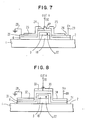
- FIG. 7 The separation of the contact area above the gate 3 and the external application of the semiconductor layer are illustrated in FIG. 7 where complementary n and p conductivity type devices are produced.
- FIG. 7 again the same reference numerals are employed for the same elements in the figures.
- On the substrate 1 on surface 2 a gate 3 with terminal 22 is positioned.
- An insulating layer 6 is provided that is conformal over the gate 3 and on the surface 2 on each side.
- a first n conductivity type transistor has as its source electrode 23 and as drain electrode 24.
- the metal employed for electrodes 23 and 24 is selected for good contact to n conductivity type semiconductor material.
- the p conductivity type transistor has as source 26 and drain 27 electrodes a metal that provides a good electrical contact to p conductivity type semiconductor material.
- the semiconductor material 25 is not intentionally doped and can be converted to either n or p conductivity through a field effect by a positive or negative signal, respectively, on the gate 3 terminal 22.
- Nominally undoped semiconductor films are generally referred to in the art as intrinsic.
- One skilled in the art will know how to dope the layers to provide alternative devices with enhancement or depletion modes of operation.
- the resulting structure with the n conductivity type transistor source electrode 21 connected to reference potential through terminal 28 and the p conductivity type transistor source electrode 26 connected to +V potential through terminal 29, and with the output at 30, may serve as a logic inverter implemented by an interconnected complementary pair of transistors.
- a gate signal sensitive, continuous intrinsic semiconductor layer 31 and insulator layer 6 are conformally deposited over the prism made up of insulator 18 and gate 3, with separate deposition and erosion operations being employed for n conductivity type metal contacts 32 and 33 and for p conductivity type metal contacts 34 and 35.
- the structure when connected with terminal 28 connected to reference potential and terminal 29 to +V potential, with a gate signal applied at terminal 22 and with the output at 30 is a complementary interconnected pair of self-aligned transistors that may be employed as a logic inverter.
- the preferred embodiment of the invention is that of the interconnected pair of complementary transistors, as illustrated in connection with FIG. 8.
- the substrate 1 would be of supporting material that is generally insulating, for example, glass or silicon coated with oxide or nitride.
- the insulator 18 would be deposited.
- the gate 3 of conductive material such as molybdenum, chrome, nickel or nichrome, is deposited and lithographically patterned. The thickness of the order of 0.5 micrometers of the gate 3 will be selected in accordance with the desired length of the channel in the completed device.
- the essentially vertical sidewalls will be patterned by reactive ion etching of the gate 3 and spacing insulator 18 pedestal.
- the insulating layer 6 of, for example, Si3N4 or SiO2 is deposited on the surface 2 and conformally over the insulator 18 and gate 3 combination.
- the layer 31 is amorphous silicon with atomic hydrogen, known in the art as a-Si:H.
- a lithographic mask is employed to define the a-Si:H layer 31 in the device area over the source, gate and drain electrodes.
- the conformal deposition of layer 31 may be by plasma deposition from silane gas, providing a nominally intrinsic semiconductor layer 31 that can be gate modulated to form either n-channel or p-channel.
- a lithographically defined mask is employed to uncover the area for contacts 32 and 33.
- An evaporated metallization of MgAl or a TiAl bilayer which makes good n contact is produced by a vaporization direction with an incidence that is normal to the surface 2.
- the contacts 32 and 33 are then separated by a dip etch to a depth sufficient to remove the metal on the vertical sidewalls.
- a lithographically defined mask is then employed to cover contacts 32 and 33 and permit deposition of contacts 34 and 35 which are separated by a dip etch to remove the metal on the vertical sidewall.
- the metal chosen for contacts 34 and 35 is selected for good p contact, such as Au, Pt, Pd or other high work function metal.
- the thickness of contacts 32 and 34 should approximately equal the difference in thickness between insulator 18 and the combined thickness of insulator 6 and semiconductor layer 31.
- an additional insulating layer is added as illustrated in connection with Fig. 5 to reduce the parasitic capacitances between gate 3 and contacts 33 and 35.
- a mask is then used to control an etching operation that exposes the source and drain electrodes to the contacts 32, 33, 34 and 35.
- the principle of the invention provides alternate fabrication techniques.
- the gate is formed on the substrate and conformal coatings of insulator and semiconductor are provided over it.
- a metal is deposited from the direction normal to the surface that is thicker in the horizontal dimension than the vertical so as to be susceptible to an erosion operation such as a dip etch which separates the metal into self-aligned contact areas on each side of a semiconductor device channel.
- the gate is formed on a pedestal positioned on the substrate.
- the gate insulator is conformally coated over the combination of the gate and the pedestal.
- a non-conformal deposition of the source and drain electrodes is then made on the horizontal surfaces by directional evaporation followed by a dip etch without masking.
- An amorphous silicon semiconductor film is conformally deposited over the pedestal and gate combination with the source and drain electrodes in place. Contacts through the amorphous silicon film are then lithographically defined to configure circuits as desired.
- gate capacitance can be further controlled through placing a spacer over the gate.
Landscapes
- Thin Film Transistor (AREA)
- Bipolar Transistors (AREA)
- Recrystallisation Techniques (AREA)
- Electrodes Of Semiconductors (AREA)
Applications Claiming Priority (2)
| Application Number | Priority Date | Filing Date | Title |
|---|---|---|---|
| US06/889,137 US4757361A (en) | 1986-07-23 | 1986-07-23 | Amorphous thin film transistor device |
| US889137 | 1986-07-23 |
Publications (3)
| Publication Number | Publication Date |
|---|---|
| EP0254071A2 true EP0254071A2 (fr) | 1988-01-27 |
| EP0254071A3 EP0254071A3 (en) | 1988-06-15 |
| EP0254071B1 EP0254071B1 (fr) | 1992-05-20 |
Family
ID=25394567
Family Applications (1)
| Application Number | Title | Priority Date | Filing Date |
|---|---|---|---|
| EP87109211A Expired EP0254071B1 (fr) | 1986-07-23 | 1987-06-26 | Dispositif transistor à couche mince amorphe |
Country Status (4)
| Country | Link |
|---|---|
| US (1) | US4757361A (fr) |
| EP (1) | EP0254071B1 (fr) |
| JP (1) | JPS6333870A (fr) |
| DE (1) | DE3779202D1 (fr) |
Cited By (2)
| Publication number | Priority date | Publication date | Assignee | Title |
|---|---|---|---|---|
| GB2285334A (en) * | 1993-12-30 | 1995-07-05 | At & T Corp | Thin film transistor having increased effective channel width |
| WO2016200626A1 (fr) * | 2015-06-12 | 2016-12-15 | Eastman Kodak Company | Transistors à couches minces verticaux et planaires sur un substrat commun |
Families Citing this family (9)
| Publication number | Priority date | Publication date | Assignee | Title |
|---|---|---|---|---|
| EP0270323B1 (fr) * | 1986-11-29 | 1999-11-03 | Sharp Kabushiki Kaisha | Méthode de fabrication d'un transistor en couche mince |
| JP2602132B2 (ja) * | 1991-08-09 | 1997-04-23 | 三菱電機株式会社 | 薄膜電界効果素子およびその製造方法 |
| KR0136931B1 (ko) * | 1994-05-12 | 1998-04-24 | 문정환 | 박막 트랜지스터의 구조 및 제조방법 |
| US6995053B2 (en) * | 2004-04-23 | 2006-02-07 | Sharp Laboratories Of America, Inc. | Vertical thin film transistor |
| US7629633B2 (en) * | 2004-05-20 | 2009-12-08 | Isaac Wing Tak Chan | Vertical thin film transistor with short-channel effect suppression |
| JP2009130165A (ja) * | 2007-11-26 | 2009-06-11 | Sanyo Electric Co Ltd | Cmos半導体装置 |
| US8709920B2 (en) * | 2011-02-24 | 2014-04-29 | Semiconductor Energy Laboratory Co., Ltd. | Method for manufacturing semiconductor device |
| KR102576428B1 (ko) | 2016-04-29 | 2023-09-08 | 삼성디스플레이 주식회사 | 어레이 기판, 이를 포함하는 액정 표시 장치 및 어레이 기판의 제조 방법 |
| US11245038B2 (en) * | 2017-03-30 | 2022-02-08 | Intel Corporation | Vertical multi-gate thin film transistors |
Family Cites Families (14)
| Publication number | Priority date | Publication date | Assignee | Title |
|---|---|---|---|---|
| JPS53142189A (en) * | 1977-05-17 | 1978-12-11 | Matsushita Electronics Corp | Insulating gate type field effect transistor |
| US4422090A (en) * | 1979-07-25 | 1983-12-20 | Northern Telecom Limited | Thin film transistors |
| JPS5731179A (en) * | 1980-07-31 | 1982-02-19 | Sharp Corp | Formation of thin-film transistor |
| JPS5790977A (en) * | 1980-11-27 | 1982-06-05 | Seiko Epson Corp | Double-layer gate polysilicon mos transistor |
| EP0098111B1 (fr) * | 1982-06-24 | 1989-08-09 | Harris Semiconductor Patents, Inc. | Transistor à effet de champ à porte isolée et procédé pour sa fabrication |
| US4554570A (en) * | 1982-06-24 | 1985-11-19 | Rca Corporation | Vertically integrated IGFET device |
| JPS59106172A (ja) * | 1982-12-07 | 1984-06-19 | インタ−ナシヨナル ビジネス マシ−ンズ コ−ポレ−シヨン | 電界効果トランジスタの製造方法 |
| EP0121068B1 (fr) * | 1983-03-31 | 1988-01-13 | BBC Brown Boveri AG | Dispositif semi-conducteur de puissance et méthode de fabrication |
| US4554572A (en) * | 1983-06-17 | 1985-11-19 | Texas Instruments Incorporated | Self-aligned stacked CMOS |
| US4547789A (en) * | 1983-11-08 | 1985-10-15 | Energy Conversion Devices, Inc. | High current thin film transistor |
| JPS60111456A (ja) * | 1983-11-22 | 1985-06-17 | Toshiba Corp | 半導体記憶装置 |
| JPS60160169A (ja) * | 1984-01-30 | 1985-08-21 | Sony Corp | Mosトランジスタおよびその製造方法 |
| DE3581549D1 (de) * | 1984-03-12 | 1991-03-07 | Xerox Corp | Duennfilm-transistor fuer hohe spannungen. |
| JPS61271873A (ja) * | 1985-05-27 | 1986-12-02 | Toppan Printing Co Ltd | 電界効果型薄膜トランジスタ |
-
1986
- 1986-07-23 US US06/889,137 patent/US4757361A/en not_active Expired - Fee Related
-
1987
- 1987-05-08 JP JP62110916A patent/JPS6333870A/ja active Granted
- 1987-06-26 EP EP87109211A patent/EP0254071B1/fr not_active Expired
- 1987-06-26 DE DE8787109211T patent/DE3779202D1/de not_active Expired - Lifetime
Cited By (2)
| Publication number | Priority date | Publication date | Assignee | Title |
|---|---|---|---|---|
| GB2285334A (en) * | 1993-12-30 | 1995-07-05 | At & T Corp | Thin film transistor having increased effective channel width |
| WO2016200626A1 (fr) * | 2015-06-12 | 2016-12-15 | Eastman Kodak Company | Transistors à couches minces verticaux et planaires sur un substrat commun |
Also Published As
| Publication number | Publication date |
|---|---|
| JPH0558674B2 (fr) | 1993-08-27 |
| US4757361A (en) | 1988-07-12 |
| EP0254071B1 (fr) | 1992-05-20 |
| JPS6333870A (ja) | 1988-02-13 |
| EP0254071A3 (en) | 1988-06-15 |
| DE3779202D1 (de) | 1992-06-25 |
Similar Documents
| Publication | Publication Date | Title |
|---|---|---|
| US4954855A (en) | Thin film transistor formed on insulating substrate | |
| US5140388A (en) | Vertical metal-oxide semiconductor devices | |
| US4633284A (en) | Thin film transistor having an annealed gate oxide and method of making same | |
| US4753897A (en) | Method for providing contact separation in silicided devices using false gate | |
| US4547789A (en) | High current thin film transistor | |
| US4333224A (en) | Method of fabricating polysilicon/silicon junction field effect transistors | |
| JPH10209468A (ja) | Soi半導体デバイス | |
| US4757361A (en) | Amorphous thin film transistor device | |
| US5702987A (en) | Method of manufacture of self-aligned JFET | |
| US4037307A (en) | Methods for making transistor structures | |
| US20040031981A1 (en) | Self-aligned vertical gate semiconductor device | |
| EP0020929A1 (fr) | Transistors à effet de champ | |
| US4546366A (en) | Polysilicon/silicon junction field effect transistors and integrated circuits (POSFET) | |
| EP0113059B1 (fr) | Méthode pour former un conducteur de largeur submicronique et méthode pour former un transistor à effet de champ comprenant un tel conducteur comme électrode de porte | |
| US4631568A (en) | Bipolar transistor construction | |
| EP0122004A2 (fr) | Construction d'un transistor bipolaire | |
| US4542577A (en) | Submicron conductor manufacturing | |
| US4713355A (en) | Bipolar transistor construction | |
| US5231296A (en) | Thin film transistor structure with insulating mask | |
| JPH059941B2 (fr) | ||
| US3700976A (en) | Insulated gate field effect transistor adapted for microwave applications | |
| JPH06163905A (ja) | 絶縁ゲート半導体装置の製造方法 | |
| JPH05267683A (ja) | 半導体不揮発性記憶装置の製造方法 | |
| KR900005870B1 (ko) | 반도체 장치의 접속구조 | |
| JPH05343413A (ja) | バイポーラトランジスタとその製造方法 |
Legal Events
| Date | Code | Title | Description |
|---|---|---|---|
| PUAI | Public reference made under article 153(3) epc to a published international application that has entered the european phase |
Free format text: ORIGINAL CODE: 0009012 |
|
| AK | Designated contracting states |
Kind code of ref document: A2 Designated state(s): DE FR GB IT |
|
| PUAL | Search report despatched |
Free format text: ORIGINAL CODE: 0009013 |
|
| AK | Designated contracting states |
Kind code of ref document: A3 Designated state(s): DE FR GB IT |
|
| 17P | Request for examination filed |
Effective date: 19880530 |
|
| 17Q | First examination report despatched |
Effective date: 19910218 |
|
| GRAA | (expected) grant |
Free format text: ORIGINAL CODE: 0009210 |
|
| AK | Designated contracting states |
Kind code of ref document: B1 Designated state(s): DE FR GB IT |
|
| PG25 | Lapsed in a contracting state [announced via postgrant information from national office to epo] |
Ref country code: IT Free format text: LAPSE BECAUSE OF FAILURE TO SUBMIT A TRANSLATION OF THE DESCRIPTION OR TO PAY THE FEE WITHIN THE PRESCRIBED TIME-LIMIT;WARNING: LAPSES OF ITALIAN PATENTS WITH EFFECTIVE DATE BEFORE 2007 MAY HAVE OCCURRED AT ANY TIME BEFORE 2007. THE CORRECT EFFECTIVE DATE MAY BE DIFFERENT FROM THE ONE RECORDED. Effective date: 19920520 |
|
| REF | Corresponds to: |
Ref document number: 3779202 Country of ref document: DE Date of ref document: 19920625 |
|
| ET | Fr: translation filed | ||
| PLBE | No opposition filed within time limit |
Free format text: ORIGINAL CODE: 0009261 |
|
| STAA | Information on the status of an ep patent application or granted ep patent |
Free format text: STATUS: NO OPPOSITION FILED WITHIN TIME LIMIT |
|
| 26N | No opposition filed | ||
| PGFP | Annual fee paid to national office [announced via postgrant information from national office to epo] |
Ref country code: FR Payment date: 19960607 Year of fee payment: 10 |
|
| PGFP | Annual fee paid to national office [announced via postgrant information from national office to epo] |
Ref country code: DE Payment date: 19960628 Year of fee payment: 10 |
|
| PGFP | Annual fee paid to national office [announced via postgrant information from national office to epo] |
Ref country code: GB Payment date: 19970523 Year of fee payment: 11 |
|
| PG25 | Lapsed in a contracting state [announced via postgrant information from national office to epo] |
Ref country code: FR Free format text: LAPSE BECAUSE OF NON-PAYMENT OF DUE FEES Effective date: 19980227 |
|
| PG25 | Lapsed in a contracting state [announced via postgrant information from national office to epo] |
Ref country code: DE Free format text: LAPSE BECAUSE OF NON-PAYMENT OF DUE FEES Effective date: 19980303 |
|
| REG | Reference to a national code |
Ref country code: FR Ref legal event code: ST |
|
| REG | Reference to a national code |
Ref country code: FR Ref legal event code: ST |
|
| PG25 | Lapsed in a contracting state [announced via postgrant information from national office to epo] |
Ref country code: GB Free format text: LAPSE BECAUSE OF NON-PAYMENT OF DUE FEES Effective date: 19980626 |
|
| GBPC | Gb: european patent ceased through non-payment of renewal fee |
Effective date: 19980626 |