EP0254312B1 - Verfahren und Anlage zur Herstellung von Diamanten - Google Patents
Verfahren und Anlage zur Herstellung von Diamanten Download PDFInfo
- Publication number
- EP0254312B1 EP0254312B1 EP87110686A EP87110686A EP0254312B1 EP 0254312 B1 EP0254312 B1 EP 0254312B1 EP 87110686 A EP87110686 A EP 87110686A EP 87110686 A EP87110686 A EP 87110686A EP 0254312 B1 EP0254312 B1 EP 0254312B1
- Authority
- EP
- European Patent Office
- Prior art keywords
- substrate
- diamond
- grid
- radiating material
- plasma
- Prior art date
- Legal status (The legal status is an assumption and is not a legal conclusion. Google has not performed a legal analysis and makes no representation as to the accuracy of the status listed.)
- Expired - Lifetime
Links
- 229910003460 diamond Inorganic materials 0.000 title claims description 117
- 239000010432 diamond Substances 0.000 title claims description 117
- 238000000034 method Methods 0.000 title claims description 39
- 230000002194 synthesizing effect Effects 0.000 title claims description 24
- 239000000758 substrate Substances 0.000 claims description 96
- 239000000463 material Substances 0.000 claims description 70
- 239000007789 gas Substances 0.000 claims description 39
- OKTJSMMVPCPJKN-UHFFFAOYSA-N Carbon Chemical compound [C] OKTJSMMVPCPJKN-UHFFFAOYSA-N 0.000 claims description 25
- 238000000576 coating method Methods 0.000 claims description 22
- 229910052799 carbon Inorganic materials 0.000 claims description 20
- 239000002994 raw material Substances 0.000 claims description 18
- 239000011248 coating agent Substances 0.000 claims description 14
- 230000004913 activation Effects 0.000 claims description 11
- 239000000203 mixture Substances 0.000 claims description 11
- 230000000694 effects Effects 0.000 claims description 10
- WFKWXMTUELFFGS-UHFFFAOYSA-N tungsten Chemical compound [W] WFKWXMTUELFFGS-UHFFFAOYSA-N 0.000 claims description 9
- 229910052721 tungsten Inorganic materials 0.000 claims description 9
- 239000010937 tungsten Substances 0.000 claims description 9
- 239000004615 ingredient Substances 0.000 claims description 8
- 239000004215 Carbon black (E152) Substances 0.000 claims description 6
- 229910002804 graphite Inorganic materials 0.000 claims description 6
- 239000010439 graphite Substances 0.000 claims description 6
- 229930195733 hydrocarbon Natural products 0.000 claims description 6
- 150000002430 hydrocarbons Chemical class 0.000 claims description 6
- VZGDMQKNWNREIO-UHFFFAOYSA-N tetrachloromethane Chemical compound ClC(Cl)(Cl)Cl VZGDMQKNWNREIO-UHFFFAOYSA-N 0.000 claims description 6
- ZOKXTWBITQBERF-UHFFFAOYSA-N Molybdenum Chemical compound [Mo] ZOKXTWBITQBERF-UHFFFAOYSA-N 0.000 claims description 5
- 150000001875 compounds Chemical class 0.000 claims description 5
- 229910052750 molybdenum Inorganic materials 0.000 claims description 5
- 239000011733 molybdenum Substances 0.000 claims description 5
- 239000007787 solid Substances 0.000 claims description 4
- UFHFLCQGNIYNRP-UHFFFAOYSA-N Hydrogen Chemical compound [H][H] UFHFLCQGNIYNRP-UHFFFAOYSA-N 0.000 claims description 3
- 239000011203 carbon fibre reinforced carbon Substances 0.000 claims description 3
- 239000001257 hydrogen Substances 0.000 claims description 3
- 229910052739 hydrogen Inorganic materials 0.000 claims description 3
- 230000001376 precipitating effect Effects 0.000 claims description 3
- 239000012808 vapor phase Substances 0.000 claims description 3
- 125000004435 hydrogen atom Chemical group [H]* 0.000 claims description 2
- -1 or LaBs Chemical compound 0.000 claims description 2
- 229910052715 tantalum Inorganic materials 0.000 claims description 2
- GUVRBAGPIYLISA-UHFFFAOYSA-N tantalum atom Chemical compound [Ta] GUVRBAGPIYLISA-UHFFFAOYSA-N 0.000 claims description 2
- 150000001721 carbon Chemical group 0.000 claims 1
- 238000005520 cutting process Methods 0.000 description 16
- 238000005268 plasma chemical vapour deposition Methods 0.000 description 11
- 238000002474 experimental method Methods 0.000 description 10
- 238000006243 chemical reaction Methods 0.000 description 9
- 229910003481 amorphous carbon Inorganic materials 0.000 description 8
- 238000005229 chemical vapour deposition Methods 0.000 description 8
- 150000002500 ions Chemical class 0.000 description 8
- 238000001816 cooling Methods 0.000 description 7
- 238000012360 testing method Methods 0.000 description 7
- 239000002245 particle Substances 0.000 description 6
- 238000001237 Raman spectrum Methods 0.000 description 3
- 125000004432 carbon atom Chemical group C* 0.000 description 3
- 238000010835 comparative analysis Methods 0.000 description 3
- 238000010168 coupling process Methods 0.000 description 3
- 238000005859 coupling reaction Methods 0.000 description 3
- 230000001419 dependent effect Effects 0.000 description 3
- 238000010438 heat treatment Methods 0.000 description 3
- 238000009413 insulation Methods 0.000 description 3
- 238000004519 manufacturing process Methods 0.000 description 3
- 239000002244 precipitate Substances 0.000 description 3
- 238000000197 pyrolysis Methods 0.000 description 3
- 150000003254 radicals Chemical class 0.000 description 3
- 239000004065 semiconductor Substances 0.000 description 3
- 238000001308 synthesis method Methods 0.000 description 3
- 230000003213 activating effect Effects 0.000 description 2
- 230000015572 biosynthetic process Effects 0.000 description 2
- 238000011156 evaluation Methods 0.000 description 2
- 239000010419 fine particle Substances 0.000 description 2
- 239000010931 gold Substances 0.000 description 2
- 238000007733 ion plating Methods 0.000 description 2
- 230000008018 melting Effects 0.000 description 2
- 238000002844 melting Methods 0.000 description 2
- 238000012545 processing Methods 0.000 description 2
- 229910052710 silicon Inorganic materials 0.000 description 2
- 239000010703 silicon Substances 0.000 description 2
- 239000010936 titanium Substances 0.000 description 2
- 238000009834 vaporization Methods 0.000 description 2
- XLYOFNOQVPJJNP-UHFFFAOYSA-N water Substances O XLYOFNOQVPJJNP-UHFFFAOYSA-N 0.000 description 2
- YZCKVEUIGOORGS-IGMARMGPSA-N Protium Chemical compound [1H] YZCKVEUIGOORGS-IGMARMGPSA-N 0.000 description 1
- RTAQQCXQSZGOHL-UHFFFAOYSA-N Titanium Chemical compound [Ti] RTAQQCXQSZGOHL-UHFFFAOYSA-N 0.000 description 1
- XAGFODPZIPBFFR-UHFFFAOYSA-N aluminium Chemical compound [Al] XAGFODPZIPBFFR-UHFFFAOYSA-N 0.000 description 1
- 229910052782 aluminium Inorganic materials 0.000 description 1
- 238000004458 analytical method Methods 0.000 description 1
- 239000013590 bulk material Substances 0.000 description 1
- 239000000470 constituent Substances 0.000 description 1
- 239000013078 crystal Substances 0.000 description 1
- 230000003247 decreasing effect Effects 0.000 description 1
- 230000000593 degrading effect Effects 0.000 description 1
- 238000010586 diagram Methods 0.000 description 1
- 239000012776 electronic material Substances 0.000 description 1
- 238000001704 evaporation Methods 0.000 description 1
- 230000008020 evaporation Effects 0.000 description 1
- 239000007888 film coating Substances 0.000 description 1
- 238000009501 film coating Methods 0.000 description 1
- 239000012530 fluid Substances 0.000 description 1
- PCHJSUWPFVWCPO-UHFFFAOYSA-N gold Chemical compound [Au] PCHJSUWPFVWCPO-UHFFFAOYSA-N 0.000 description 1
- 229910052737 gold Inorganic materials 0.000 description 1
- 238000000227 grinding Methods 0.000 description 1
- 239000012535 impurity Substances 0.000 description 1
- 230000002401 inhibitory effect Effects 0.000 description 1
- 238000010884 ion-beam technique Methods 0.000 description 1
- WCYWZMWISLQXQU-UHFFFAOYSA-N methyl Chemical compound [CH3] WCYWZMWISLQXQU-UHFFFAOYSA-N 0.000 description 1
- 230000007935 neutral effect Effects 0.000 description 1
- 239000012071 phase Substances 0.000 description 1
- 238000001020 plasma etching Methods 0.000 description 1
- 238000001556 precipitation Methods 0.000 description 1
- 230000001737 promoting effect Effects 0.000 description 1
- 239000010453 quartz Substances 0.000 description 1
- 230000005855 radiation Effects 0.000 description 1
- 239000003507 refrigerant Substances 0.000 description 1
- VYPSYNLAJGMNEJ-UHFFFAOYSA-N silicon dioxide Inorganic materials O=[Si]=O VYPSYNLAJGMNEJ-UHFFFAOYSA-N 0.000 description 1
- 238000003786 synthesis reaction Methods 0.000 description 1
- 229910052719 titanium Inorganic materials 0.000 description 1
Images

Classifications
-
- C—CHEMISTRY; METALLURGY
- C30—CRYSTAL GROWTH
- C30B—SINGLE-CRYSTAL GROWTH; UNIDIRECTIONAL SOLIDIFICATION OF EUTECTIC MATERIAL OR UNIDIRECTIONAL DEMIXING OF EUTECTOID MATERIAL; REFINING BY ZONE-MELTING OF MATERIAL; PRODUCTION OF A HOMOGENEOUS POLYCRYSTALLINE MATERIAL WITH DEFINED STRUCTURE; SINGLE CRYSTALS OR HOMOGENEOUS POLYCRYSTALLINE MATERIAL WITH DEFINED STRUCTURE; AFTER-TREATMENT OF SINGLE CRYSTALS OR A HOMOGENEOUS POLYCRYSTALLINE MATERIAL WITH DEFINED STRUCTURE; APPARATUS THEREFOR
- C30B25/00—Single-crystal growth by chemical reaction of reactive gases, e.g. chemical vapour-deposition growth
- C30B25/02—Epitaxial-layer growth
-
- C—CHEMISTRY; METALLURGY
- C30—CRYSTAL GROWTH
- C30B—SINGLE-CRYSTAL GROWTH; UNIDIRECTIONAL SOLIDIFICATION OF EUTECTIC MATERIAL OR UNIDIRECTIONAL DEMIXING OF EUTECTOID MATERIAL; REFINING BY ZONE-MELTING OF MATERIAL; PRODUCTION OF A HOMOGENEOUS POLYCRYSTALLINE MATERIAL WITH DEFINED STRUCTURE; SINGLE CRYSTALS OR HOMOGENEOUS POLYCRYSTALLINE MATERIAL WITH DEFINED STRUCTURE; AFTER-TREATMENT OF SINGLE CRYSTALS OR A HOMOGENEOUS POLYCRYSTALLINE MATERIAL WITH DEFINED STRUCTURE; APPARATUS THEREFOR
- C30B29/00—Single crystals or homogeneous polycrystalline material with defined structure characterised by the material or by their shape
- C30B29/02—Elements
- C30B29/04—Diamond
Definitions
- the present invention relates to an improved vaporphase diamond synthesizing method, more particularly, to a method of synthesizing extremely consummate crystalline diamond which is almost free from carbon ingredient having structure other than diamond.
- the diamond film growth rate is not yet sufficient.
- any of those prior arts cited earlier can generate diamond almost being free from amorphous carbon and graphite having structure other than diamond as being identified by Raman spectrum method, while featuring extremely high electric resistance and cnsummation degree.
- any method generating non-polar discharge of microwaves inside of the reactive tube which vertically penetrates a conventional waveguide tube due to short wavelength of microwaves, if a reaction tube has a diameter longer than the wavelength of microwaves is made available, since this system cannot perfectly seal microwaves and causes microwaves to leak out of the reaction tube, the diameter of the reaction tube is constrained by the wavelength of microwaves, thus making it difficult for the reaction tube to provide wide coating zone and resulting in the difficulty to implement mass production.
- Japanese industries normally use 915 MHz and 2,350 MHz of industrial frequencies. These frequencies constrain the diameter of the reaction tube within a maximum of 120 mm and 50 mm, respectively. Consequently, these diameters are not sufficient for generating a large-dimension coating zone durable for implementing mass production on the industrial basis.
- RF plasma CVD method in order to generate extremely consummate diamond, the system needs to generate extremely intensified plasma. Only the induction-coupling type RF power-supply source is actually made available for exciting plasma. It should be noted that capacity-coupling type RF power-supply source cannot synthesize crystalline diamond except for amorphous diamond.
- the system in order to generate a large-dimension coating zone by applying RF induction-coupling type power-supply source, the system should be provided with an extremely large-capacity RF power-supply source which in turn involves much difficulty in the industrial application.
- thermoelectron radi-ating material CVD method can process a large number of diamond and implement coating of a large area as well.
- this prior art still has problems to solve, in which more amount of carbon other than diamond is present in the synthesized diamond than the amount of carbon present in the diamond synthesized by the microwave plasma CVD method, thus eventually degrading the degree of the consummation of diamond itself, while also causing electric resistance to lower.
- thermoelectron radiating material CVD was quite advantageous for implementing mass production of diamond film
- inventors followed up efforts for establishing a method of improving the quality of diamond film.
- the invention relates to a method of synthesizing diamond, which is substantially the method of synthesizing diamond by applying low-pressurized vapor phase for causing diamond to precipitate itself on the surface of substrate heated to 600 ° C through 1,200 ° C by activating raw-material gas which is composed of the mixture of hydrogen with solid carbon, or hydrocarbon, or hydrocarbon containing O and N in the bonded radical, or carbon tetrachloride, wherein the method is comprised of the sequential steps of; activating the above raw-material gas by applying thermoelectron radiating material heated to a minimum of 1,600°C, providing potential by connecting positive electrode to grid disposed between thermoelectron radiating material which is provided with negative electrode and the substrate to be treated with coating process by applying DC power-supply source; extracting thermoelectrons for generating plasma; providing potential by connecting the positive and negative electrodes to the grid and the substrate by applying another DC power-supply source; generating plasma by holding the potential of the substrate negative in order that the effect of the activation generated by thermoele
- extremely consummate diamond film denotes the one having a maximum of 2 microns of mean particle size, while the diamond film is mainly composed of surface (111) having a minimum of 1010 ⁇ -cm of electric resistance.
- the diamond film may also be provided with surfaces (100) or (110) as well, due to convenience of tools, diamond surface should desirably be provided with surface (111).
- electric resistance normally indicates a certain amount of residual carbon. In other words, the higher the electric resistance, the less is the amount of residual carbon such as amorphous carbon and graphite.
- FIG. 2 is the constitution of the substrate holding base improved from the one used for the preferred embodiment of the invention, which is provided with cooling device. Arrowed directions respectively denote the flow path of refrigerant.
- the cooling device properly adjusts temperature of the substrate by allowing fluid like water and/or gas to flow through it. It is also possible for the improved substrate holding base to more precisely control temperature by internally providing a temperature-measuring instrument in part of the substrate or the substrate holding base.
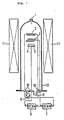
- FIG. 1 is the simplified block diagram of a preferred embodiment of the apparatus for implementing the method of synthesizing diamond related to the invention.
- CH 4 and H 2 mixed gas are led into quartz- made reaction tube 12 via raw-material gas inlet 1, and then, the mixed gas is thermally activated by thermoelectron radiating material 2 heated to more than 1,600 ° C.
- the apparatus causes negative electrode and positive electrode to respectively be connected to thermoelectron radiating material 2 and grid 3 by applying DC power-supply source 7 so that plasma can be generated between thermoelectron radiating material which has extracted thermoelectrons from thermoelectron radiating material 2 and the grid 3.
- the substrate 4 is then held in the negative potential so that the positive ion can positively be drawn onto the surface of the substrate 4 by allowing the negative electrode to be connected to the substrate 4 on the holding base 5. While executing these processes, the system uses extremely pressurized gas ranging from a minimum of 10 Torr to a maximum of 400 Torr.
- the apparatus shown in FIG. 1 is provided with AC power-supply source 6 for heating thermoelectron radiating material, vacuum exhaust outlet 9, insulation seal 10, and external furnace 11, respectively.
- the invention provides four features which are summarized below.
- thermoelectrons In order to stably generate and maintain plasma by applying such an extremely high pressure ranging from a minimum of 10 Torr to a maximum of 400 Torr, it is essential for the system to extract thermoelectrons from thermoelectron radiating material.
- thermoelectron radiating material When feeding negative potential to the substrate, if the negative electrode and the positive electrode were respectively connected to the substrate and thermoelectron radiating material by applying DC power-supply source, thermoelectrons cannot be extracted from thermoelectron radiating material but conversely thermoelectrons will be set back, and as a result, no plasma can be generated under presence of such a high pressure mentioned above.
- the apparatus related to the invention disposes a grid between thermoelectron radiating material and the substrate so that plasma can be generated between these members by allowing thermoelectrons to be extracted from thermoelectron radiating material after connecting the negative electrode to thermoelectron radiating material and the positive electrode to the grid by applying DC power-supply source. Furthermore, the apparatus causes the already-generated positive ion to be drawn onto the substrate and generates plasma by respectively connecting the positive electrode and the negative electrode to the grid and the substrate by applying another DC power-supply source.
- the invention allows generation of DC plasma in addition to the pyrolysis and the activation of raw-material gas done by thermoelectron radiating material in order that the degree of activation can securely be promoted.
- This intensifies energy of the activated gas and causes the gas volume remaining in the activated state to increase itself, where the activated gas includes hydrogen radical capable of selectively eliminating carbon (other than diamond) precipitating itself together with diamond and/or methyl radical having SP 3 mixed track needed for generating diamond.
- the life of the activated gas is durable, graphite and/or amorphous carbon having structure other than diamond can be prevented from precipitating itself, thus eventually allowing such extremely consummate diamond film to be generated securely.
- the diamond synthesis method related to the invention proved to have generated significantly fine composition of the diamond film which was formed on the surface of the substrate. It is probable that both the impact of ion against the surface of the substrate and the plasma generated on the surface of the substrate advantageously affected the degree of activation of the activated ingredients, concentration, and the life of these activated ingredients as well, thus eventually promoting the density of the diamond nucleus being generated.
- the invention securely provides an extremely consummate diamond film which is free from such carbon matter having shape other than diamond and features a maximum of 1 micron of fine constitution of the diamond film even after being exposed to a minimum of 1,000 ° C of high temperature by generating extremely intensified bonding strength against the substrate.
- the method of synthesizing diamond related to the invention allows the use of carbon ingredients, for example, such as solid carbon, or hydrocarbon, or hydrocarbon containing O and N in the bonded radical, or carbon tetrachloride. It is possible for the diamond synthesis method related to the invention to effectively use raw-material gas composed of the mixture of at least more than one kind of those carbon ingredients and hydrogen. When solid carbon is made available for carbon source, it is desirable for the system to use carbon for making up thermoelectron radiating material.
- the proportional rate of carbon atoms present in the raw-material gas is less than 0.01 %, diamond film will grow itself at an extremely slow rate, which is not durable enough for actual use. Conversely, if the proportional rate of carbon atoms in the raw-material gas exceeds 20%, compared to diamond, a greater amount of carbon having structure other than diamond will precipitate itself, thus eventually inhibiting formation of diamond film.
- Ar, Kr, Xe, Rn, and N 2 which are respectively independent of the reaction may also be used in mixture with those gas ingredients mentioned above.
- Ar, Kr, Xe, Rn, and N 2 which are respectively independent of the reaction may also be used in mixture with those gas ingredients mentioned above.
- Each of these can effectively be used for cooling down temperature of the substrate owing to low thermal conductivity, and yet, each properly adjusts the strength of plasma as another phase of advantage.
- thermoelectron radiating material and the grid material it is essential for the thermoelectron radiating material and the grid material to provide low-vapor pressure under presence of high temperature and have high melting point as well.
- thermoelectron radiating material it is essential for thermoelectron radiating material to be superb in the capacity of releasing thermoelectrons. Consequently, it is desirable that both the thermoelectron radiating material and the grid be made from those materials having high melting point like tungsten (W), tantalum (Ta), or molybdenum(Mo), or LaBs, or graphite, for example.
- Thermoelectron radiating material should be used only after being heated to a minimum of 1,600 ° C of ultra-high temperature. If temperature goes down from 1,600 ° C, graphite and amorphous carbon will dominantly precipitate themselves. Unless the surface of the substrate bears a minimum of 600°C and a maximum of 1,200°C, diamond does not precipitate at all.
- Reactor should internally be provided with a minimum of 10 Torr and a maximum of 400 Torr of pressure, preferably the internal pressure should a minimum of 50 Torr and a maximum of 300 Torr. If the pressure inside of the reactor exceeds 400 Torr, it is difficult for the apparatus related to the invention to stably maintain plasma between the grid and the substrate. Conversely, if the pressure inside of the reactor is lower than 10 Torr, evaporation speed will significantly lower, thus generating unwanted results.
- the invention features the capability of stably generating and maintaining plasma under presence of high pressure, which cannot actually be realized by any conventional system that merely uses DC power-supply source. This is because the expansion of gas pressure effectively promotes the density of the generated diamond nucleus.
- the intensity of plasma generated between thermoelectron radiating material and the grid is dependent on the gas atmosphere, configuration of thermoelectron radiating material and grid, temperature of thermoelectron radiating material, arrangement of thermoelectron radiating material and grid, and the power output from DC power-supply source. Since the plasma radiation is observed in the position close to the grid, it is desirable for the apparatus to properly control the plasma-generating condition by applying DC power-supply source which is delivered per unit area of the grid.
- the apparatus When embodying the invention, it is desirable for the apparatus to feed a minimum of 10 W/cm 2 of DC power between the thermoelectron radiating material and the grid. If the apparatus receives less than 10 W/cm 2 of DC power, the apparatus cannot stably generate and maintain plasma between the grid and the substrate. Furthermore, the intensity of plasma generated between the grid and the substrate is dependent on the intensity of plasma generated between thermoelectron radiating material and grid, gas atmosphere, configuration of the grid, substrate, and the substrate holding base, arrangement of the grid and the substrate, and the power output from DC power-supply source. Like the above case, since plasma is generated in the position close to the grid and the surface of the substrate facing the grid, it is desirable for the apparatus to properly control the plasma by applying DC power-supply source delivered per unit area of the substrate surface to be coated.
- the apparatus related to the invention should desirably feed a minimum of 5 W/cm2 and a maximum of 200 W/cm 2 of DC power between the thermoelectron radiating material and the grid. If less than 5 W/cm2 of DC power is delivered, the apparatus will not be able to stably generate and maintain plasma between the grid and the substrate. Conversely, if more than 200 W/cm 2 of DC power is delivered, the plasma etching effect will be magnified, thus extremely slowing down the diamond precipitation speed.
- Temperature on the surface of the substrate is dependent on the temperature of thermoelectron radi- ating material, arrangement and configuration of thermoelectron radiating material, grid, and the substrate, DC power being delivered between the thermoelectron radiating material and the grid, DC power being delivered between the grid and the substrate, gas atmosphere, and temperature of the external furnace, etc.
- the optimum effect of the invention is generated by properly selecting specific conditions from those mentioned above.
- the diamond synthesizing apparatus related to the invention may execute operations for cooling down temperature of the substrate holding base and the wall of the reactor in order to precisely constrain temperature on the surface of the substrate within an adequate range. Control of temperature on the surface of substrate is extremely important for the apparatus related to the invention in order to correctly control stress which remains on the diamond film.
- tungsten(W)-made filament which substantially made up thermoelectron radiating material
- inventors once heated the compound gas to more than 2,000 ° C in order that temperature on the surface of the substrate could be adjusted to 920°C.
- Inventors arranged the distance between tungsten filament and grid made from tungsten to be 5 mm and also the distance between tungsten filament and molybdenum-made substrate of the grid to be 4 mm, respectively.
- Table 1 represents the coating conditions and characteristic of the coated film. Depending on the coating conditions, inventors adjusted temperature on the surface of the substrate by cooling down temperature borne by the substrate holding base.
- the second preferred embodiment of the invention By implementing the second preferred embodiment of the invention, extremely consummate diamond surpassing that is achieved by the microwave plasma CVD method featuring a maximum of 1 micron of fine particle size and unsurpassed strength of bonding with the substrate is securely generated even under exposure to a minimum of 1,000 ° C of high temperature.
- the second preferred embodiment of the invention it is possible for the second preferred embodiment of the invention to execute processing of a plurality of substrates and coating process over a wide area by applying a plurality of thermoelectron radiating materials.
- thermoelectron radiating materials which were also made available for implementing the first preferred embodiment.
- heating power sources were independently provided so that temperature of each thermoelectron radiating material could independently be controlled.
- DC power-supply source one-side of the electrodes were commonly connected to each other.
- the size of the grid disposed between the thermoelectron radiating material and the substrate was 220 mm x 180 mm.
- the second preferred embodiment of the invention successfully generated diamond film having 8 ⁇ m in average of thickness with a maximum of 10% of unevenness.
- Each crystalline particle had an extremely fine size ranging from 0.3 micron to a maximum of 0.8 micron.
- Evaluation of electric resistance resulted in quite satisfactory values ranging from 10 11 to a maximum of 1012 ⁇ •crn.
- inventors employed the substrate made from SPG 422 type ISO K-10 cemented carbide. Using the same apparatus as that was employed for the first preferred embodiment, inventors executed coating of substrate with diamond film. Inventors arranged the distance between the filament and the grid to be 5 mm and the distance between the grid and the upper surface of the insert to be 4 mm, respectively.
- Test No. 27 merely generated amorphous carbon.
- thermoelectron radiating material CVD the preferred embodiments of the invention respectively activate raw-material compound gas by applying thermoelectron radiating material being heated to a minimum of 1,600°C, and then, using a DC power-supply source, potential is generated for the diamond synthesizing apparatus by connecting thermoelectron radiating material to the negative electrode and the grid to the positive electrode, in which the grid is disposed between the thermoelectron radiating material and the substrate subject to coating with diamond film, thus allowing thermoelectrons to be extracted from this material so that plasma can eventually be generated.
- the apparatus related to the invention also uses another DC power-supply source for generating potential by connecting the grid and the substrate to the positive and negative electrodes for generating plasma while holding the substrate potential negative.
- the apparatus jointly uses activation generated by thermoelectron radiating material and the other activation caused by generation of DC plasma, and yet, by properly controlling pressure inside of the reactor to a minimum of 10 Torr and a maximum of 400 Torr for causing plasma to be generated, the apparatus securely generates extremely consummate diamond which is significantly better in quality than that which is normally generated by the thermoelectron radiating material CVD method.
- the apparatus related to the invention provides diamond with significantly satisfactory electric resistance which is incomparable to that which is normally generated by the microwave plasma CVD method, the diamond which is synthesized by the method and the apparatus related to the invention is usefully applicable to a wide variety of electronic materials requiring extremely satisfactory insulation effect such as heat-radiating printed wiring boards and diamond semiconductors for example.
- the method and the apparatus related to the invention securely provide fine-particle-size diamond film even under the presence of high temperature above 1000 ° C with extremely strong bonding effect against the substrate, the method and the apparatus for synthesizing diamond related to the invention securely and significantly improve the productivity by effectively being applied to those uses which effectively utilize mechanical characteristic of diamond such as cutting tools and wear-resistant parts for example.
Landscapes
- Chemical & Material Sciences (AREA)
- Engineering & Computer Science (AREA)
- Crystallography & Structural Chemistry (AREA)
- Materials Engineering (AREA)
- Metallurgy (AREA)
- Organic Chemistry (AREA)
- Chemical Kinetics & Catalysis (AREA)
- General Chemical & Material Sciences (AREA)
- Crystals, And After-Treatments Of Crystals (AREA)
- Chemical Vapour Deposition (AREA)
Claims (6)
Applications Claiming Priority (4)
| Application Number | Priority Date | Filing Date | Title |
|---|---|---|---|
| JP173366/86 | 1986-07-23 | ||
| JP17336686A JPH0649635B2 (ja) | 1986-07-23 | 1986-07-23 | ダイヤモンドの合成方法 |
| JP75282/87 | 1987-03-27 | ||
| JP62075282A JPS63241323A (ja) | 1987-03-27 | 1987-03-27 | 表面温度測定方法 |
Publications (2)
| Publication Number | Publication Date |
|---|---|
| EP0254312A1 EP0254312A1 (de) | 1988-01-27 |
| EP0254312B1 true EP0254312B1 (de) | 1990-11-07 |
Family
ID=26416433
Family Applications (1)
| Application Number | Title | Priority Date | Filing Date |
|---|---|---|---|
| EP87110686A Expired - Lifetime EP0254312B1 (de) | 1986-07-23 | 1987-07-23 | Verfahren und Anlage zur Herstellung von Diamanten |
Country Status (4)
| Country | Link |
|---|---|
| US (1) | US4859490A (de) |
| EP (1) | EP0254312B1 (de) |
| KR (1) | KR910001359B1 (de) |
| DE (1) | DE3766029D1 (de) |
Cited By (10)
| Publication number | Priority date | Publication date | Assignee | Title |
|---|---|---|---|---|
| EP0327051A1 (de) * | 1988-02-01 | 1989-08-09 | Sumitomo Electric Industries Limited | Diamant und seine Darstellung durch ein Verfahren mittels Abscheidung aus der Gasphase |
| FR2635535A1 (fr) * | 1988-08-22 | 1990-02-23 | Gen Electric | Element chauffant perfectionne a resistance pour la fabrication de diamant par deposition en phase gazeuse par procede chimique |
| EP0365366A1 (de) * | 1988-10-21 | 1990-04-25 | Crystallume | Gleichmässiger, dünner Diamantfilm sowie ein Verfahren zu dessen Herstellung |
| US5146481A (en) * | 1991-06-25 | 1992-09-08 | Diwakar Garg | Diamond membranes for X-ray lithography |
| US5270028A (en) * | 1988-02-01 | 1993-12-14 | Sumitomo Electric Industries, Ltd. | Diamond and its preparation by chemical vapor deposition method |
| EP0574263A1 (de) * | 1992-06-11 | 1993-12-15 | General Electric Company | Diamantfilme mittels CVD |
| EP0607987A3 (de) * | 1993-01-22 | 1995-11-29 | Norton Co | Verfahren zum Herstellen eines Diamantfilmes und dessen Verwendung. |
| US5909879A (en) * | 1993-03-09 | 1999-06-08 | Norton Company | Diamond film coating for mating parts |
| US5993919A (en) * | 1996-12-04 | 1999-11-30 | Sumitomo Electric Industries, Ltd. | Method of synthesizing diamond |
| US6161499A (en) * | 1997-07-07 | 2000-12-19 | Cvd Diamond Corporation | Apparatus and method for nucleation and deposition of diamond using hot-filament DC plasma |
Families Citing this family (26)
| Publication number | Priority date | Publication date | Assignee | Title |
|---|---|---|---|---|
| US5079031A (en) * | 1988-03-22 | 1992-01-07 | Semiconductor Energy Laboratory Co., Ltd. | Apparatus and method for forming thin films |
| US5006203A (en) * | 1988-08-12 | 1991-04-09 | Texas Instruments Incorporated | Diamond growth method |
| US5258206A (en) * | 1989-01-13 | 1993-11-02 | Idemitsu Petrochemical Co., Ltd. | Method and apparatus for producing diamond thin films |
| US4953499A (en) * | 1989-08-03 | 1990-09-04 | General Electric Company | Apparatus for synthetic diamond deposition including curved filaments and substrate cooling means |
| JPH0780718B2 (ja) * | 1989-08-04 | 1995-08-30 | トヨタ自動車株式会社 | ダイヤモンドの合成方法および合成装置 |
| US5075094A (en) * | 1990-04-30 | 1991-12-24 | The United States Of America As Represented By The Secretary Of The Navy | Method of growing diamond film on substrates |
| DE4029268C2 (de) * | 1990-09-14 | 1995-07-06 | Balzers Hochvakuum | Verfahren zur gleichspannungs-bogenentladungs-unterstützten, reaktiven Behandlung von Gut und Vakuumbehandlungsanlage zur Durchführung |
| DE4029270C1 (de) * | 1990-09-14 | 1992-04-09 | Balzers Ag, Balzers, Li | |
| US5147687A (en) * | 1991-05-22 | 1992-09-15 | Diamonex, Inc. | Hot filament CVD of thick, adherent and coherent polycrystalline diamond films |
| CA2077773A1 (en) * | 1991-10-25 | 1993-04-26 | Thomas R. Anthony | Microwave, rf, or ac/dc discharge assisted flame deposition of cvd diamond |
| EP0549187A1 (de) * | 1991-12-26 | 1993-06-30 | General Electric Company | Diamant-Überzüge |
| EP0549207A1 (de) * | 1991-12-26 | 1993-06-30 | General Electric Company | Diamant-Überzüge |
| US5290610A (en) * | 1992-02-13 | 1994-03-01 | Motorola, Inc. | Forming a diamond material layer on an electron emitter using hydrocarbon reactant gases ionized by emitted electrons |
| US5359170A (en) * | 1992-02-18 | 1994-10-25 | At&T Global Information Solutions Company | Apparatus for bonding external leads of an integrated circuit |
| JP3041133B2 (ja) * | 1992-06-01 | 2000-05-15 | 松下電器産業株式会社 | イオン化蒸着装置 |
| US5431963A (en) * | 1993-02-01 | 1995-07-11 | General Electric Company | Method for adhering diamondlike carbon to a substrate |
| US5441013A (en) * | 1993-03-23 | 1995-08-15 | At&T Bell Laboratories | Method for growing continuous diamond films |
| JP2595894B2 (ja) * | 1994-04-26 | 1997-04-02 | 日本電気株式会社 | 水素ラジカル発生装置 |
| US5711773A (en) * | 1994-11-17 | 1998-01-27 | Plasmoteg Engineering Center | Abrasive material for precision surface treatment and a method for the manufacturing thereof |
| US5976206A (en) * | 1995-05-19 | 1999-11-02 | Saint-Gobain/Norton Industrial Ceramics Corporation | Method of making white diamond film |
| US6126793A (en) | 1995-10-17 | 2000-10-03 | Citizen Watch Co., Ltd. | Method of forming films over inner surface of cylindrical member |
| US5776553A (en) * | 1996-02-23 | 1998-07-07 | Saint Gobain/Norton Industrial Ceramics Corp. | Method for depositing diamond films by dielectric barrier discharge |
| US20080241413A1 (en) * | 2007-03-26 | 2008-10-02 | Ravi Kramadhati V | Plasma tool for forming porous diamond films for semiconductor applications |
| GB0813491D0 (en) | 2008-07-23 | 2008-08-27 | Element Six Ltd | Diamond Material |
| GB0813490D0 (en) | 2008-07-23 | 2008-08-27 | Element Six Ltd | Solid state material |
| BE1019439A3 (fr) * | 2010-07-30 | 2012-07-03 | Diarotech | Procede pour synthetiser par depot chimique en phase vapeur une matiere solide, en particulier du diamant, ainsi qu'un dispositif pour l'application du procede. |
Family Cites Families (5)
| Publication number | Priority date | Publication date | Assignee | Title |
|---|---|---|---|---|
| US4434188A (en) * | 1981-12-17 | 1984-02-28 | National Institute For Researches In Inorganic Materials | Method for synthesizing diamond |
| JPS60122794A (ja) * | 1983-12-01 | 1985-07-01 | Mitsubishi Metal Corp | ダイヤモンドの低圧気相合成法 |
| JPS60221395A (ja) * | 1984-04-19 | 1985-11-06 | Yoshio Imai | ダイヤモンド薄膜の製造方法 |
| DE3587881T2 (de) * | 1984-11-29 | 1995-03-02 | Matsushita Electric Ind Co Ltd | Verfahren zur plasma-chemischen Abscheidung aus der Dampfphase und Verfahren zur Herstellung eines Films von diamantähnlichem Kohlenstoff. |
| JP3196906B2 (ja) * | 1992-08-21 | 2001-08-06 | 富士ゼロックス株式会社 | 画像信号の符号化装置 |
-
1987
- 1987-07-20 US US07/075,470 patent/US4859490A/en not_active Expired - Fee Related
- 1987-07-23 DE DE8787110686T patent/DE3766029D1/de not_active Expired - Lifetime
- 1987-07-23 EP EP87110686A patent/EP0254312B1/de not_active Expired - Lifetime
- 1987-07-23 KR KR1019870008023A patent/KR910001359B1/ko not_active Expired
Non-Patent Citations (1)
| Title |
|---|
| PATENT ABSTRACTS OF JAPAN, vol. 9, no. 200 (C-298)[1923], 16th August 1985; & JP-A-60 70 178 (NIPPON DENSHIN DENWA KOSHA) 20-04-1985 * |
Cited By (13)
| Publication number | Priority date | Publication date | Assignee | Title |
|---|---|---|---|---|
| US5270028A (en) * | 1988-02-01 | 1993-12-14 | Sumitomo Electric Industries, Ltd. | Diamond and its preparation by chemical vapor deposition method |
| EP0327051A1 (de) * | 1988-02-01 | 1989-08-09 | Sumitomo Electric Industries Limited | Diamant und seine Darstellung durch ein Verfahren mittels Abscheidung aus der Gasphase |
| FR2635535A1 (fr) * | 1988-08-22 | 1990-02-23 | Gen Electric | Element chauffant perfectionne a resistance pour la fabrication de diamant par deposition en phase gazeuse par procede chimique |
| US5607723A (en) * | 1988-10-21 | 1997-03-04 | Crystallume | Method for making continuous thin diamond film |
| EP0365366A1 (de) * | 1988-10-21 | 1990-04-25 | Crystallume | Gleichmässiger, dünner Diamantfilm sowie ein Verfahren zu dessen Herstellung |
| US5146481A (en) * | 1991-06-25 | 1992-09-08 | Diwakar Garg | Diamond membranes for X-ray lithography |
| EP0574263A1 (de) * | 1992-06-11 | 1993-12-15 | General Electric Company | Diamantfilme mittels CVD |
| US5523121A (en) * | 1992-06-11 | 1996-06-04 | General Electric Company | Smooth surface CVD diamond films and method for producing same |
| EP0607987A3 (de) * | 1993-01-22 | 1995-11-29 | Norton Co | Verfahren zum Herstellen eines Diamantfilmes und dessen Verwendung. |
| US5909879A (en) * | 1993-03-09 | 1999-06-08 | Norton Company | Diamond film coating for mating parts |
| US5993919A (en) * | 1996-12-04 | 1999-11-30 | Sumitomo Electric Industries, Ltd. | Method of synthesizing diamond |
| US6161499A (en) * | 1997-07-07 | 2000-12-19 | Cvd Diamond Corporation | Apparatus and method for nucleation and deposition of diamond using hot-filament DC plasma |
| US6200652B1 (en) | 1997-07-07 | 2001-03-13 | Cvd Diamond Corporation | Method for nucleation and deposition of diamond using hot-filament DC plasma |
Also Published As
| Publication number | Publication date |
|---|---|
| US4859490A (en) | 1989-08-22 |
| KR880001524A (ko) | 1988-04-23 |
| EP0254312A1 (de) | 1988-01-27 |
| DE3766029D1 (de) | 1990-12-13 |
| KR910001359B1 (ko) | 1991-03-04 |
Similar Documents
| Publication | Publication Date | Title |
|---|---|---|
| EP0254312B1 (de) | Verfahren und Anlage zur Herstellung von Diamanten | |
| KR910001367B1 (ko) | 기상 합성 다이아몬드막 및 그 합성방법 | |
| EP0797688B1 (de) | Verfahren zum aufbringen diamantähnlicher kohlenstoff-filme | |
| US5370912A (en) | Diamond film deposition with a microwave plasma | |
| JPH06279185A (ja) | ダイヤモンド結晶およびダイヤモンド結晶膜の形成方法 | |
| US5110405A (en) | Method of manufacturing single-crystal diamond particles | |
| JP3194820B2 (ja) | 配向性ダイヤモンド膜の形成方法 | |
| US5200231A (en) | Method of manufacturing polycrystalline diamond layers | |
| US8334027B2 (en) | Method for DC plasma assisted chemical vapor deposition in the absence of a positive column | |
| US5993919A (en) | Method of synthesizing diamond | |
| WO1990005701A1 (en) | Diamond production | |
| JP2501589B2 (ja) | 気相合成ダイヤモンドおよびその合成方法 | |
| JP2001506572A (ja) | 気相合成によるダイヤモンド皮膜の形成方法 | |
| US5087478A (en) | Deposition method and apparatus using plasma discharge | |
| EP0230927A2 (de) | Herstellung von Diamant | |
| JPH0649635B2 (ja) | ダイヤモンドの合成方法 | |
| JP2780497B2 (ja) | CVD法によるSi基板へのダイヤモンド膜形成方法 | |
| KR910001360B1 (ko) | 다이아몬드 벌크재의 합성방법 | |
| JPS6395200A (ja) | 硬質窒化ホウ素膜の製造方法 | |
| Naseem et al. | High pressure high power microwave plasma chemical vapor deposition of large area diamond films | |
| JPH0518794B2 (de) | ||
| JPH0733580B2 (ja) | 立方晶系窒化ホウ素膜の製造方法 | |
| Pai et al. | Low-pressure chemical vapour deposition of diamond films in a radio-frequency-plasma-assisted hot-filament reactor | |
| JPH04240189A (ja) | CVD法によるSi基板へのダイヤモンド膜形成方法 | |
| JP2780494B2 (ja) | CVD法によるSi基板へのダイヤモンド膜形成方法 |
Legal Events
| Date | Code | Title | Description |
|---|---|---|---|
| PUAI | Public reference made under article 153(3) epc to a published international application that has entered the european phase |
Free format text: ORIGINAL CODE: 0009012 |
|
| AK | Designated contracting states |
Kind code of ref document: A1 Designated state(s): DE FR GB SE |
|
| 17P | Request for examination filed |
Effective date: 19880226 |
|
| RAP3 | Party data changed (applicant data changed or rights of an application transferred) |
Owner name: SUMITOMO ELECTRIC INDUSTRIES, LIMITED |
|
| 17Q | First examination report despatched |
Effective date: 19890418 |
|
| GRAA | (expected) grant |
Free format text: ORIGINAL CODE: 0009210 |
|
| AK | Designated contracting states |
Kind code of ref document: B1 Designated state(s): DE FR GB SE |
|
| REF | Corresponds to: |
Ref document number: 3766029 Country of ref document: DE Date of ref document: 19901213 |
|
| ET | Fr: translation filed | ||
| PLBE | No opposition filed within time limit |
Free format text: ORIGINAL CODE: 0009261 |
|
| STAA | Information on the status of an ep patent application or granted ep patent |
Free format text: STATUS: NO OPPOSITION FILED WITHIN TIME LIMIT |
|
| 26N | No opposition filed | ||
| EAL | Se: european patent in force in sweden |
Ref document number: 87110686.0 |
|
| PGFP | Annual fee paid to national office [announced via postgrant information from national office to epo] |
Ref country code: FR Payment date: 19950711 Year of fee payment: 9 |
|
| PGFP | Annual fee paid to national office [announced via postgrant information from national office to epo] |
Ref country code: GB Payment date: 19950712 Year of fee payment: 9 |
|
| PGFP | Annual fee paid to national office [announced via postgrant information from national office to epo] |
Ref country code: SE Payment date: 19950717 Year of fee payment: 9 |
|
| PGFP | Annual fee paid to national office [announced via postgrant information from national office to epo] |
Ref country code: DE Payment date: 19950725 Year of fee payment: 9 |
|
| PG25 | Lapsed in a contracting state [announced via postgrant information from national office to epo] |
Ref country code: GB Effective date: 19960723 |
|
| PG25 | Lapsed in a contracting state [announced via postgrant information from national office to epo] |
Ref country code: SE Effective date: 19960724 |
|
| GBPC | Gb: european patent ceased through non-payment of renewal fee |
Effective date: 19960723 |
|
| PG25 | Lapsed in a contracting state [announced via postgrant information from national office to epo] |
Ref country code: FR Effective date: 19970328 |
|
| PG25 | Lapsed in a contracting state [announced via postgrant information from national office to epo] |
Ref country code: DE Effective date: 19970402 |
|
| EUG | Se: european patent has lapsed |
Ref document number: 87110686.0 |
|
| REG | Reference to a national code |
Ref country code: FR Ref legal event code: ST |