EP0258051A2 - Processeur de signal numérique à fonction de division - Google Patents
Processeur de signal numérique à fonction de division Download PDFInfo
- Publication number
- EP0258051A2 EP0258051A2 EP87307564A EP87307564A EP0258051A2 EP 0258051 A2 EP0258051 A2 EP 0258051A2 EP 87307564 A EP87307564 A EP 87307564A EP 87307564 A EP87307564 A EP 87307564A EP 0258051 A2 EP0258051 A2 EP 0258051A2
- Authority
- EP
- European Patent Office
- Prior art keywords
- signal
- significant bit
- accumulator
- bit section
- digital
- Prior art date
- Legal status (The legal status is an assumption and is not a legal conclusion. Google has not performed a legal analysis and makes no representation as to the accuracy of the status listed.)
- Granted
Links
Images

Classifications
-
- G—PHYSICS
- G06—COMPUTING OR CALCULATING; COUNTING
- G06F—ELECTRIC DIGITAL DATA PROCESSING
- G06F7/00—Methods or arrangements for processing data by operating upon the order or content of the data handled
- G06F7/38—Methods or arrangements for performing computations using exclusively denominational number representation, e.g. using binary, ternary, decimal representation
- G06F7/48—Methods or arrangements for performing computations using exclusively denominational number representation, e.g. using binary, ternary, decimal representation using non-contact-making devices, e.g. tube, solid state device; using unspecified devices
- G06F7/52—Multiplying; Dividing
- G06F7/535—Dividing only
-
- G—PHYSICS
- G06—COMPUTING OR CALCULATING; COUNTING
- G06F—ELECTRIC DIGITAL DATA PROCESSING
- G06F2207/00—Indexing scheme relating to methods or arrangements for processing data by operating upon the order or content of the data handled
- G06F2207/535—Indexing scheme relating to groups G06F7/535 - G06F7/5375
- G06F2207/5352—Non-restoring division not covered by G06F7/5375
Definitions
- This invention relates to a digital signal processor and more particularly to one in which the division of an N-bit positive dividend by a positive divisor can be executed in N+1 processor cycles.
- Digital signal processors utilizing a microcomputer have been developed to perform a variety of tasks more efficiently than can generally be achieved utilizing a general purpose microprocessor.
- One standard division technique employed in such digital signal processors utilizes a radix 2 non-restoring divide algorithm.
- Such a known operation utilizes the sequence shown in TABLE I with the results of each processing step being repetitively stored in two accumulators to derive the final quotient and remainder.
- step 1 of TABLE I an accumulator ACC1 which will eventually hold the remainder R, is initialized to 0.
- step 2a the remainder R is first tested to determine whether it is less than 0. Both the current R and Q values in accumulators ACC1 and ACC0 respectively, are then doubled and the most significant bit q of the dividend d currently stored in the accumulator ACC0, is added to the remainder R. Then depending upon the results of the test on the remainder R, the divisor D is either added to or subtracted from the current value of the remainder R to derive a new value for the remainder which is again stored in accumulator ACC1.
- step 2b if the current value of the remainder R is negative, the quotient Q in the accumulator ACC0 remains the same. On the other hand if the value of R is greater than or equal to 0 the value of the quotient Q in the accumulator ACC0 is incremented by 1.
- step 3 is performed once to restore the remainder R to a positive value if the current value in the accumulator ACC1 is negative.
- the values of R and Q in step 2a can be doubled by shifting them one position in the registers ACC1 and ACC0. It can be seen that it is necessary to test twice for the value of R during each iteration of the divide operation, in order to determine whether D should be added to or subtracted from R as detailed in step 2a, and then whether the quotient Q should remain the same or be incremented by 1 as detailed in step 2b. Hence using this standard technique, the remainder R must be tested twice during each step of the divide operation. Because it is necessary to test the value of R twice during each iteration of step 2, the number of instruction cycles is essentially double the number of binary bits in the dividend d. Step 3 is needed to restore the remainder to a positive value should the result in accumulator ACC1 be negative after step 2 is iterated n times.
- a digital signal processor for dividing a digital dividend signal by a digital divisor signal to obtain a digital quotient signal and a digital remainder signal.
- the processor comprises an arithmetic logic unit having selectively concatenated independently controllable most significant bit and least significant bit sections, an accumulator and a shift register. The respective outputs of the sections of the accumulator are connected to those of the inputs of the shift register while the output of the shift register is coupled through the arithmetic logic unit back to the inputs of the sections of the accumulator.
- the digital signal processor also comprises a control means for controlling the division of the digital dividend signal as follows: a) - loading the dividend signal into the least significant bit section of the accumulator; b) - in the arithmetic logic unit, testing whether the current value of the digital signal from the most significant bit section of the accumulator is negative; c) shifting the concatenated signal from the accumulator in the shift register to double the value thereof; d) - if the test in b) is true, adding in the arithmetic logic unit, the value of the divisor signal to the current value of the signal from the most significant bit section of the shift register and storing the resultant signal in the most significant bit section of the accumulator; e) - also if the test in b) is true, incrementing in the arithmetic logic unit, the value of the signal from the least significant bit section of the shift register by 1 and storing the resultant signal in the least significant bit section of the accumulator; f) - else if the test in b
- the quotient digit resulting from each processor cycle is either a "1" or "0". This can be determined by subtracting the divisor from the remainder and looking at the sign of the result. If it is negative, the divisor must be added back on to restore the remainder, and the quotient bit is set to "0". If it is zero or positive, the new remainder becomes the resultant of the subtraction and the quotient bit is set to "1". As in all longhand division, a digit is then brought down after each step. As a result N such steps must be carried out for the division of a N bit positive binary dividend. The bringing down of a binary digit effectively doubles the remainder and adds the new digit to it.
- each processing cycle of the division requires two consecutive tests for the value of the remainder R.
- the second test has been eliminated by utilizing a modified division algorithm with a modified digital signal processor to perform this function. This can be better understood by reference to TABLE II which shows the division algorithm of the present invention.
- step 2 of TABLE II a test is then made to determine whether the current value of R in the accumulator ACC1 is less than 0 by checking whether its negative signbit is set.
- the current values of the remainder R and quotient Q are doubled and the most significant bit (MSB) stored in accumulator ACC0 is added to that of ACC1.
- MSB most significant bit
- This is readily achieved in a single operation by shifting the entire signal from the output of the accumulator ACC one bit position as it enters the register SR.
- the value of the divisor D is then added to that of the remainder R, and the result again stored in accumulator ACC0 while the value of the quotient Q is incremented by 1.
- the divisor D is subtracted from that of the remainder R while the quotient Q remains unchanged. Step 2 is repeated N times which is equal to the number of bits in the dividend d.
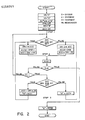
- step 3 if the remainder R is negative, the value of the divisor D is added to it to restore the remainder to a positive integer. Also, to obtain the correct value of the quotient Q, its current value is again doubled in the accumulator ACC1 and then incremented by 1 by repeating step 2. This results in the complement value which can be readily inverted to derive the correct output. In step 3, if the remainder R is not negative, the current value of the remainder R is correct. The value of the quotient Q is obtained by repeating step 2 and inverting the result. As a result, the division of an N bit binary dividend can be completed in N+1 operation cycles as opposed to 2N+1 cycles for the division algorithm defined in TABLE I. This is achieved by utilizing a modified digital signal processor of the type illustrated in Figure 1 when programmed to use the flow chart sequence illustrated in Figure 2.
- the digital signal processor includes an arithmetic unit 5 in which a 16 bit digital dividend signal d is loaded into an XR register 10 from input data received through a bus 11.
- the divisor signal D is then loaded into a YR register 12 again through received data from the bus 11.
- the dividend signal d is also coupled to an N cycle counter 13 where the number of significant bits of the 16 bit word are initially determined.
- the dividend signal d from the XR register 10 is transferred through a multiplexer 14 to the least significant bit section SR0 of a 32 bit shift register 15.
- the most significant bit section SR1 of the shift register 15 is concurrently initialized to 0.
- This entire binary signal is then transferred from the SR0 and SR1 sections of the register 15 through an arithmetic logic unit (ALU) 20 on a 32 bit bus to the ACC0 and ACC1 sections respectively of an accumulator 21 to complete the initialization step 1 of TABLE II.
- ALU arithmetic logic unit
- the ALU 20 is formed from two conventional 16 bit independently controllable units, one of which provides the most significant bit (MSB) section and the other the least significant bit (LSB) section.
- the ALU 20 MSB and LSB sections can be selectively concatenated to perform two 16 bit operations or one 32 bit operation with accumulator ACC0 holding the least significant bits and accumulator ACC1 holding the most significant bits of the binary result signal.
- the arithmetic logic unit 20 checks to determine whether the accumulator's negative signbit is set thus indicating a negative number. The initial test will of course always result in the answer being false because accumulator ACC1 was initialized to 0. Regardless of the result, the entire signal from the accumulator 21 is transferred to the input of the shift register 15 and is then doubled by moving it one position towards the most significant bit end of the register 15. During this stage both the least and most significant bit sections SR0 and SR1 of the register 15 are concatenated. This automatically results in the most significant bit of the dividend d in the shift register SR0 being added to the current value of the remainder R in the shift register SR1.
- step 2 of the flow chart in Figure 2 when there is a false test result, the binary signal in the SR0 section of the register 15 is then transferred (via the arithmetic logic unit 20) to the ACC0 section of the accumulator 21, while the divisor D from the register YR 12 is subtracted from the binary signal in the most significant bit section of the register 15 (in the unit 20) with the result being stored in the accumulator ACC1.
- step 2 of Table II determines that the result stored in the accumulator is negative, thus a true test result
- the current value of the quotient Q in the shift register SR0 is incremented by 1 while the divisor D from the register YR, is added to the current value of the remainder R. This latter step restores the remainder to a positive integer.
- step 2 of the division algorithm is repeated N+1 times where N is equal to the number of binary bits in the dividend d.
- a second test is then performed to determine whether the count remaining is equal to 1. If not, step 2 of TABLE II is repeated. After N iterations of this step, the algorithm enters step 3.
- step 3 the current value of the remainder R in the accumulator ACC1 is again tested to determine whether it is negative. If the remainder test proves false, the value in the shift register 15 is transferred directly to the accumulator 21 so as to derive the final value of the remainder R at the output of accumulator ACC1. On the other hand, if the test is true indicating that the current value of the remainder R is negative, the divisor D is again added to the remainder R to restore it to a positive value and derive the final value of the remainder R. Step 2 is then repeated one more time to obtain the complemented value of the quotient Q at the output of the accumulator ACC0.
- the correct value of the quotient Q can then be obtained by inverting the output of the accumulator ACC0. It is to be noted that the portions of Step 2 affecting accumulaor ACC1 need not be carried out during this final step since the remainder "R" has already been determined. However repeating the complete step simplifies the overall algorithm.
- the ALU 20 is divided into two selectively concatenated independently controllable sections so that the values can be selectively processed to achieve one of these requirements.
- the complement of the quotient Q is stored in the accumulator ACC0. In this way both halves of the ALU 20 simultaneously perform an add (+D, +1) or a subtract (-D, -0) step.
- the actual value of the quotient Q can also be readily obtained at the output of the accumulator ACC0 by taking the complement of its value upon completion of the division algorithm. In many storage registers both values are accessible directly from the register.
Landscapes
- Physics & Mathematics (AREA)
- General Physics & Mathematics (AREA)
- Engineering & Computer Science (AREA)
- Computational Mathematics (AREA)
- Mathematical Analysis (AREA)
- Mathematical Optimization (AREA)
- Pure & Applied Mathematics (AREA)
- Theoretical Computer Science (AREA)
- Computing Systems (AREA)
- General Engineering & Computer Science (AREA)
- Complex Calculations (AREA)
- Test And Diagnosis Of Digital Computers (AREA)
Applications Claiming Priority (2)
| Application Number | Priority Date | Filing Date | Title |
|---|---|---|---|
| CA517133 | 1986-08-28 | ||
| CA000517133A CA1252213A (fr) | 1986-08-28 | 1986-08-28 | Processeur de signaux numeriques a fonction de division |
Publications (3)
| Publication Number | Publication Date |
|---|---|
| EP0258051A2 true EP0258051A2 (fr) | 1988-03-02 |
| EP0258051A3 EP0258051A3 (en) | 1990-09-19 |
| EP0258051B1 EP0258051B1 (fr) | 1993-04-28 |
Family
ID=4133827
Family Applications (1)
| Application Number | Title | Priority Date | Filing Date |
|---|---|---|---|
| EP87307564A Expired - Lifetime EP0258051B1 (fr) | 1986-08-28 | 1987-08-26 | Processeur de signal numérique à fonction de division |
Country Status (5)
| Country | Link |
|---|---|
| US (1) | US4761758A (fr) |
| EP (1) | EP0258051B1 (fr) |
| JP (1) | JP2579321B2 (fr) |
| CA (1) | CA1252213A (fr) |
| DE (1) | DE3785624T2 (fr) |
Cited By (3)
| Publication number | Priority date | Publication date | Assignee | Title |
|---|---|---|---|---|
| EP0443679A1 (fr) * | 1990-02-23 | 1991-08-28 | Koninklijke Philips Electronics N.V. | Procédé de codage selon la méthode dite RSA, par un microcontrôleur et dispositif utilisant ce procédé |
| EP0379998A3 (fr) * | 1989-01-24 | 1992-05-13 | Oki Electric Industry Co., Ltd. | Diviseur pour l'exécution d'une opération arithmétique à grande vitesse |
| GB2296350A (en) * | 1994-12-21 | 1996-06-26 | Advanced Risc Mach Ltd | Data processing divider enabling reduced interrupt latency |
Families Citing this family (3)
| Publication number | Priority date | Publication date | Assignee | Title |
|---|---|---|---|---|
| US4878190A (en) * | 1988-01-29 | 1989-10-31 | Texas Instruments Incorporated | Floating point/integer processor with divide and square root functions |
| US6125380A (en) * | 1998-04-13 | 2000-09-26 | Winbond Electronics Corporation | Dividing method |
| US7230550B1 (en) * | 2006-05-16 | 2007-06-12 | Motorola, Inc. | Low-complexity bit-robust method and system for combining codewords to form a single codeword |
Family Cites Families (8)
| Publication number | Priority date | Publication date | Assignee | Title |
|---|---|---|---|---|
| US3293418A (en) * | 1964-07-08 | 1966-12-20 | Control Data Corp | High speed divider |
| DE1774289A1 (de) * | 1968-05-17 | 1971-09-09 | Elektronische Rechenmasch Ind | Verfahren und Vorrichtung zur binaeren Division |
| US4238833A (en) * | 1979-03-28 | 1980-12-09 | Monolithic Memories, Inc. | High-speed digital bus-organized multiplier/divider system |
| US4320464A (en) * | 1980-05-05 | 1982-03-16 | Control Data Corporation | Binary divider with carry-save adders |
| DE3066955D1 (en) * | 1980-06-24 | 1984-04-19 | Ibm | Signal processor computing arrangement and method of operating said arrangement |
| JPS6054070A (ja) * | 1983-09-02 | 1985-03-28 | Nec Corp | 演算装置 |
| JPS60134343A (ja) * | 1983-12-22 | 1985-07-17 | Hitachi Ltd | 除算方式 |
| JPS60247736A (ja) * | 1984-05-24 | 1985-12-07 | Matsushita Electric Ind Co Ltd | 除算回路 |
-
1986
- 1986-08-28 CA CA000517133A patent/CA1252213A/fr not_active Expired
- 1986-09-02 US US06/902,988 patent/US4761758A/en not_active Expired - Lifetime
-
1987
- 1987-08-25 JP JP62209411A patent/JP2579321B2/ja not_active Expired - Lifetime
- 1987-08-26 EP EP87307564A patent/EP0258051B1/fr not_active Expired - Lifetime
- 1987-08-26 DE DE8787307564T patent/DE3785624T2/de not_active Expired - Fee Related
Cited By (6)
| Publication number | Priority date | Publication date | Assignee | Title |
|---|---|---|---|---|
| EP0379998A3 (fr) * | 1989-01-24 | 1992-05-13 | Oki Electric Industry Co., Ltd. | Diviseur pour l'exécution d'une opération arithmétique à grande vitesse |
| EP0443679A1 (fr) * | 1990-02-23 | 1991-08-28 | Koninklijke Philips Electronics N.V. | Procédé de codage selon la méthode dite RSA, par un microcontrôleur et dispositif utilisant ce procédé |
| FR2658932A1 (fr) * | 1990-02-23 | 1991-08-30 | Koninkl Philips Electronics Nv | Procede de codage selon la methode dite rsa, par un microcontroleur et dispositif utilisant ce procede. |
| GB2296350A (en) * | 1994-12-21 | 1996-06-26 | Advanced Risc Mach Ltd | Data processing divider enabling reduced interrupt latency |
| US5748518A (en) * | 1994-12-21 | 1998-05-05 | Advanced Risc Machines Limited | Data processing divider |
| GB2296350B (en) * | 1994-12-21 | 1999-10-06 | Advanced Risc Mach Ltd | Data processing divider |
Also Published As
| Publication number | Publication date |
|---|---|
| CA1252213A (fr) | 1989-04-04 |
| JP2579321B2 (ja) | 1997-02-05 |
| US4761758A (en) | 1988-08-02 |
| DE3785624D1 (de) | 1993-06-03 |
| EP0258051B1 (fr) | 1993-04-28 |
| JPS6362035A (ja) | 1988-03-18 |
| DE3785624T2 (de) | 1993-08-05 |
| EP0258051A3 (en) | 1990-09-19 |
Similar Documents
| Publication | Publication Date | Title |
|---|---|---|
| US4616330A (en) | Pipelined multiply-accumulate unit | |
| US4754421A (en) | Multiple precision multiplication device | |
| US5016210A (en) | Binary division of signed operands | |
| US4866652A (en) | Floating point unit using combined multiply and ALU functions | |
| FI78186B (fi) | Dataprocessor som utfoer en decimalmultiplikationsoperation under anvaendning av ett laesminne. | |
| US5426600A (en) | Double precision division circuit and method for digital signal processor | |
| EP0056525B1 (fr) | Système de division | |
| KR950006580B1 (ko) | 나눗셈연산장치 | |
| US4386413A (en) | Method and apparatus of providing a result of a numerical calculation with the number of exact significant figures | |
| EP0310701A1 (fr) | Arithmétique BCD utilisant des opérations arithmétiques et logiques binaires | |
| EP0258051B1 (fr) | Processeur de signal numérique à fonction de division | |
| JPH05250146A (ja) | 整数累乗処理を行なうための回路及び方法 | |
| US5317531A (en) | Apparatus for reducing the size of an arithmetic and logic unit necessary to practice non-restore division | |
| US5490100A (en) | Cumulative summation unit | |
| US3290493A (en) | Truncated parallel multiplication | |
| Kirchner et al. | Accurate arithmetic for vector processors | |
| US3229079A (en) | Binary divider | |
| US3056550A (en) | Variable-exponent computers | |
| US3604909A (en) | Modular unit for digital arithmetic systems | |
| US4546447A (en) | Division apparatus | |
| US5309385A (en) | Vector division processing method and system | |
| USH472H (en) | Method and apparatus for processing binary-coded/packed decimal data | |
| US3395271A (en) | Arithmetic unit for digital computers | |
| SU511590A1 (ru) | Устройство дл делени чисел | |
| GB2153559A (en) | Binary multiplication |
Legal Events
| Date | Code | Title | Description |
|---|---|---|---|
| PUAI | Public reference made under article 153(3) epc to a published international application that has entered the european phase |
Free format text: ORIGINAL CODE: 0009012 |
|
| AK | Designated contracting states |
Kind code of ref document: A2 Designated state(s): DE FR GB NL SE |
|
| PUAL | Search report despatched |
Free format text: ORIGINAL CODE: 0009013 |
|
| AK | Designated contracting states |
Kind code of ref document: A3 Designated state(s): DE FR GB NL SE |
|
| 17P | Request for examination filed |
Effective date: 19910116 |
|
| 17Q | First examination report despatched |
Effective date: 19920902 |
|
| GRAA | (expected) grant |
Free format text: ORIGINAL CODE: 0009210 |
|
| AK | Designated contracting states |
Kind code of ref document: B1 Designated state(s): DE FR GB NL SE |
|
| PG25 | Lapsed in a contracting state [announced via postgrant information from national office to epo] |
Ref country code: SE Effective date: 19930428 Ref country code: NL Effective date: 19930428 |
|
| ET | Fr: translation filed | ||
| REF | Corresponds to: |
Ref document number: 3785624 Country of ref document: DE Date of ref document: 19930603 |
|
| NLV1 | Nl: lapsed or annulled due to failure to fulfill the requirements of art. 29p and 29m of the patents act | ||
| PLBE | No opposition filed within time limit |
Free format text: ORIGINAL CODE: 0009261 |
|
| STAA | Information on the status of an ep patent application or granted ep patent |
Free format text: STATUS: NO OPPOSITION FILED WITHIN TIME LIMIT |
|
| 26N | No opposition filed | ||
| PGFP | Annual fee paid to national office [announced via postgrant information from national office to epo] |
Ref country code: FR Payment date: 19980814 Year of fee payment: 12 |
|
| PGFP | Annual fee paid to national office [announced via postgrant information from national office to epo] |
Ref country code: GB Payment date: 19980817 Year of fee payment: 12 |
|
| PGFP | Annual fee paid to national office [announced via postgrant information from national office to epo] |
Ref country code: DE Payment date: 19980907 Year of fee payment: 12 |
|
| PG25 | Lapsed in a contracting state [announced via postgrant information from national office to epo] |
Ref country code: GB Free format text: LAPSE BECAUSE OF NON-PAYMENT OF DUE FEES Effective date: 19990826 |
|
| GBPC | Gb: european patent ceased through non-payment of renewal fee |
Effective date: 19990826 |
|
| PG25 | Lapsed in a contracting state [announced via postgrant information from national office to epo] |
Ref country code: FR Free format text: LAPSE BECAUSE OF NON-PAYMENT OF DUE FEES Effective date: 20000428 |
|
| PG25 | Lapsed in a contracting state [announced via postgrant information from national office to epo] |
Ref country code: DE Free format text: LAPSE BECAUSE OF NON-PAYMENT OF DUE FEES Effective date: 20000601 |
|
| REG | Reference to a national code |
Ref country code: FR Ref legal event code: ST |