EP0258715A2 - Statischer Direktzugriffspeicher einer Bi-CMOS-Konstruktion - Google Patents
Statischer Direktzugriffspeicher einer Bi-CMOS-Konstruktion Download PDFInfo
- Publication number
- EP0258715A2 EP0258715A2 EP87111824A EP87111824A EP0258715A2 EP 0258715 A2 EP0258715 A2 EP 0258715A2 EP 87111824 A EP87111824 A EP 87111824A EP 87111824 A EP87111824 A EP 87111824A EP 0258715 A2 EP0258715 A2 EP 0258715A2
- Authority
- EP
- European Patent Office
- Prior art keywords
- transistor
- lines
- bit lines
- memory
- transistors
- Prior art date
- Legal status (The legal status is an assumption and is not a legal conclusion. Google has not performed a legal analysis and makes no representation as to the accuracy of the status listed.)
- Granted
Links
- 238000010276 construction Methods 0.000 title abstract description 6
- 230000003068 static effect Effects 0.000 title description 3
- 239000004065 semiconductor Substances 0.000 claims abstract description 8
- 230000004044 response Effects 0.000 claims abstract description 5
- 230000005669 field effect Effects 0.000 claims 5
- 238000007599 discharging Methods 0.000 abstract description 8
- 230000000295 complement effect Effects 0.000 description 13
- 230000003213 activating effect Effects 0.000 description 5
- 238000010586 diagram Methods 0.000 description 3
- 239000002184 metal Substances 0.000 description 2
- 230000002093 peripheral effect Effects 0.000 description 2
- 239000003990 capacitor Substances 0.000 description 1
- 239000000470 constituent Substances 0.000 description 1
- 230000003247 decreasing effect Effects 0.000 description 1
- 238000009792 diffusion process Methods 0.000 description 1
- 230000002349 favourable effect Effects 0.000 description 1
- 230000010354 integration Effects 0.000 description 1
- 239000011159 matrix material Substances 0.000 description 1
- 230000002035 prolonged effect Effects 0.000 description 1
- 239000000758 substrate Substances 0.000 description 1
Images



Classifications
-
- G—PHYSICS
- G11—INFORMATION STORAGE
- G11C—STATIC STORES
- G11C11/00—Digital stores characterised by the use of particular electric or magnetic storage elements; Storage elements therefor
- G11C11/21—Digital stores characterised by the use of particular electric or magnetic storage elements; Storage elements therefor using electric elements
- G11C11/34—Digital stores characterised by the use of particular electric or magnetic storage elements; Storage elements therefor using electric elements using semiconductor devices
- G11C11/40—Digital stores characterised by the use of particular electric or magnetic storage elements; Storage elements therefor using electric elements using semiconductor devices using transistors
- G11C11/41—Digital stores characterised by the use of particular electric or magnetic storage elements; Storage elements therefor using electric elements using semiconductor devices using transistors forming static cells with positive feedback, i.e. cells not needing refreshing or charge regeneration, e.g. bistable multivibrator or Schmitt trigger
- G11C11/413—Auxiliary circuits, e.g. for addressing, decoding, driving, writing, sensing, timing or power reduction
- G11C11/414—Auxiliary circuits, e.g. for addressing, decoding, driving, writing, sensing, timing or power reduction for memory cells of the bipolar type
- G11C11/416—Read-write [R-W] circuits
-
- G—PHYSICS
- G11—INFORMATION STORAGE
- G11C—STATIC STORES
- G11C11/00—Digital stores characterised by the use of particular electric or magnetic storage elements; Storage elements therefor
- G11C11/21—Digital stores characterised by the use of particular electric or magnetic storage elements; Storage elements therefor using electric elements
- G11C11/34—Digital stores characterised by the use of particular electric or magnetic storage elements; Storage elements therefor using electric elements using semiconductor devices
- G11C11/40—Digital stores characterised by the use of particular electric or magnetic storage elements; Storage elements therefor using electric elements using semiconductor devices using transistors
- G11C11/41—Digital stores characterised by the use of particular electric or magnetic storage elements; Storage elements therefor using electric elements using semiconductor devices using transistors forming static cells with positive feedback, i.e. cells not needing refreshing or charge regeneration, e.g. bistable multivibrator or Schmitt trigger
- G11C11/412—Digital stores characterised by the use of particular electric or magnetic storage elements; Storage elements therefor using electric elements using semiconductor devices using transistors forming static cells with positive feedback, i.e. cells not needing refreshing or charge regeneration, e.g. bistable multivibrator or Schmitt trigger using field-effect transistors only
-
- G—PHYSICS
- G11—INFORMATION STORAGE
- G11C—STATIC STORES
- G11C11/00—Digital stores characterised by the use of particular electric or magnetic storage elements; Storage elements therefor
- G11C11/21—Digital stores characterised by the use of particular electric or magnetic storage elements; Storage elements therefor using electric elements
- G11C11/34—Digital stores characterised by the use of particular electric or magnetic storage elements; Storage elements therefor using electric elements using semiconductor devices
- G11C11/40—Digital stores characterised by the use of particular electric or magnetic storage elements; Storage elements therefor using electric elements using semiconductor devices using transistors
- G11C11/41—Digital stores characterised by the use of particular electric or magnetic storage elements; Storage elements therefor using electric elements using semiconductor devices using transistors forming static cells with positive feedback, i.e. cells not needing refreshing or charge regeneration, e.g. bistable multivibrator or Schmitt trigger
- G11C11/413—Auxiliary circuits, e.g. for addressing, decoding, driving, writing, sensing, timing or power reduction
- G11C11/417—Auxiliary circuits, e.g. for addressing, decoding, driving, writing, sensing, timing or power reduction for memory cells of the field-effect type
- G11C11/419—Read-write [R-W] circuits
-
- G—PHYSICS
- G11—INFORMATION STORAGE
- G11C—STATIC STORES
- G11C7/00—Arrangements for writing information into, or reading information out from, a digital store
- G11C7/18—Bit line organisation; Bit line lay-out
Definitions
- the present invention relates to a semiconductor memory and, more particularly, to a random access memory of a static type having bipolar transistors and complementary MOS transistors.
- Bi-CMOS complementary metal-oxide-semiconductor
- peripheral circuits such as an address buffer, a decoder/driver, a sense amplifier and an output circuit are constructed by Bi-CMOS transistor circuits and a memory cell array is constructed by an N-channet MOS transistor circuit.
- a memory cell array of the Bi-CMOS SRAM is the same as that of a conventional SRAM constructed only by MOS transistors, and therefor an operation speed of the cell array is not improved. More specifically, a great number of memory cells are connected in common to each pair of bit lines. For this reason, these bit lines are prolonged, so that they have a large stray capacitance. One of each pair of bit lines is discharged in accordance with the data stored in a selected memory cell, and the discharging of the bit line is carried out by a MOS transistor contained in the selected memory cell.
- the MOS transistors generally have a relatively low current ability.
- the MOS transistor is formed fine to decrease the size of the memory cell. Therefore, the current ability of the MOS transistor in the memory cell is very small, so that the bit line is discharged with a large time constant. As a result, the improvement in the operation speed of the Bi-CMOS SRAM is restricted.
- an object of the present invention is to provide a semiconductor memory in which an operation speed of a memory cell portion is improved.
- Another object of the present invention is to provide a Bi-CMOS SRAM attaining a data read operation at a very high speed.
- a semiconductor memory comprises a plurality of cell blocks, each of the cell blocks including a plurality of word lines, a pair of pre-bit lines, a plurality of memory cells each connected to one of the word lines and to the pre-bit lines, first, second and third nodes, a first transistor of a bipolar type having a base connected to one of the pre-bit lines and a collector-emitter current path connected between the first and third nodes, a second transistor of the bipolar type having a base connected to the other of the pre-bit lines and a collector-emitter current path connected between the second and third nodes, and a third transistor connected between the third node and a reference point; a pair of main-bit lines connected respectively to the first and second nodes of each of the cell blocks; and means responsive to a set of address signals for selecting one of the word lines in one of the cell blocks and for turning ON the third transistor in the one of the cell blocks.
- a great number of memory cells arranged in the same column are divided into a plurality of cell blocks and the bit line is divided into the pre-bit line and the main-bit line. Accordingly, the number of memory cells connected in common to the prebit line is reduced, so that a stray capacitance of the pre-bit line is made small. The discharging of the pre-bit line is thereby carried out with a small time constant by a selected memory cell. All of the cell blocks in each column are connected to the main-bit lines whose capacitances are also reduced as compared conventional bit line structure due to the reduction in transistors connected thereto.
- the first or second transistor of the bipolar type discharges one of the main-bit lines in response to a potential difference between the pre-bit lines.
- the bipolar transistor has a large current ability. Accordingly, the discharging of the main-bit line is carried out with a small time constant. As a result, a potential difference appears between the main-bit lines within a short time in response to the data stored in the selected memory cell. The data read operation is thus performed at a high speed.
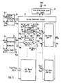
- a first embodiment of the present invention has a plurality of memory cells MC arranged in a known matrix form of N rows and M columns (N and M being integers) with N word lines in rows and M pairs of bit lines in columns.
- N and M are 256, respectively.
- the memory shown in Fig. I has 65536 memory cells.
- the memory cells MC arranged in the same row are connected in common to one of 256 word lines WL 1 to WL 256 .
- the memory cells arranged in the same column are divided into 32 cell blocks CB I-I to CB 1-32 (CB M-I to CB M-32).
- each of cell blocks includes eight memory cells, but two of them MCl and MC8 are representively illustrated in Fig. I.
- the cell blocks CB I-I to CB 1-32 (CB M-I to CB M-32) arranged in the same column are connected to a pair of main-bit lines MBL 1 and MBL 1 (MBLm and M B L m ).
- Each cell block further includes a pair of pre-bit lines SBL and SBL , a first bipolar NPN transistor Q 10 having a base connected to a true one (SBL) of the pre-bit lines, a second bipolar NPN transistor Q 11 having a base connected to a complementary one ( SBL ) of the pre-bit lines and a collect-emitter current path connected in series of the collector-emitter current path between the main-bit lines MBL and MBL as shown, a third transistor of an N-channel MOS type connected between a node of emitters of the transistors Q 10 and Q 11 and a ground terminal, and two N-channel MOS transistors Q 7 and Q 8 each connected between each of the pre-bit lines SBL and SB L and a power terminal Vcc.
- the transistor Q 12 can be replaced by an NPN bipolar transistor and the transistors Q7 and Q 8 can be replaced by resistors.
- Eight memory cells (MCI - MC8) in each cell block are connected in common to the pre-bit lines SBL and SBL .
- Each of the memory cells MC includes, as well known in the art, two N-channel MOS transistors Q 1 and Q 2 which are cross-coupled in a flip-flop form, two resistors R 1 and R 2 each operating as a load and two N-channel MOS transistors Q 3 and Q 4 each operating as a transfer gate.
- the resistors R 1 and R 2 can be replaced by a P-channel MOS transistor, respectively.
- each pair of main bit lines e.g. MSBI and M 5 B I are connected to collectors of only 32 transistors such as shown Q 10 Q 11 , respectively, although 256 memory cells are arranged in each column, and therefore capacitance of each bit line is greatly reduced as compared to the conventional bit line structure in which transistors of all the memory cells of the same column are connected to each bit line. Also, in each of cell blocks such as CB I-I, only eight transistors (Q3, Q 4 ) are connected to each pre-bit line SBL, SBL and the capacitance of each pre-bit line is extremely small.
- the bit lines are advantageously formed by diffusion regions connected to sources or drains of the transistors Q 3 , Q 4 of the memory cells in view of a high density arrangement of the memory cells in each cell block.
- the cell blocks are arranged in M columns and 32 rows and each cell block is identified by the designation CB i-j (i: address of columns, j: address of rows).
- Each word lines e.g. WLI to WL8 are extending in parallel through M cell blocks of the same rows, e.g. CB I-I to CB M-I.
- M cell blocks of the same row are selected by a row group selection signal (X 1S -X 32 ).
- the cell blocks of the first rows (CB I-I to CB M-I) are selected by the row group selection signal X 1S so that each pair of bipolar transistors Q 10 , Q 11 in the cell blocks CB I-I to CB M-I are enabled by the transistor Q 12 rendered conductive.
- the row group selection signals X is to X 32S are generated by decoding upper 5 bits of row address signals RA 1 to RA 5 by the row decoder 10.
- the row decoder 10 also decodes the remaining 3 bits of row address signals RA6 to RA8 to generate eight pre-selection signals and by performing AND logic operation of the eight pre-selection signals and each of the row group selection signals X 1S to X 32S generates selection signals X 1 to X 256 for 256 word lines WL 1 -WL 256 .
- the signals X 1 to X 8 for selecting the word lines WL 1 to WL 8 extending through the cell blocks CB I-I, CB 2-I ••• CB M-I are generated by performing AND operation on the signal X 1S and the eight pre-selection signals.
- Valid row address signals RA 1 to RA 8 are supplied to row address terminals 10-1 to 10-8 at a time point To
- the row address buffer/decoder/driver 10 responds to the valid row address data and changes one of the selection signals X 1 to X 256 to a high level. Assuming that the signal X 1 is changed to the high level, the word line W 1 is energized.
- the word line WL 1 has a relatively large stray capacitance, but the energizing thereof is completed for a short time since the row address buffer/decoder/driver 10 has a Bi-CMOS construction to present a large current ability.
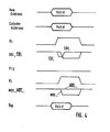
- the transistors Q 3 and Q 4 in the memory cell MC are thereby turned ON. Assuming that this memory cell MC stores a data "I" and the transistors Q 1 and Q 2 take thereby a non-conducting state and a conducting state, respectively, the complementary pre-bit line SBL is discharged by the transistor Q 2 via the transistor Q 4 to lower the potential thereof, whereas the potential of the true pre-bit line SBL is held at the high level. Since only eight memory cells are connected to the pre-bit lines SBL and SB L , the stray capacitance C SB thereof is very small. Therefore, the discharging of the complementary pre-bit line SBL is carried out with a small time constant, as shown in Fig. 2.
- the row address buffer/decoder/driver 10 further changes one of group selection selection signals X 1s to X 32S to the high level by making use of a part of the valid row address signals, i.e., RA 1 to RA 5
- Each of the selection signals X 1S to X NS is supplied to the gate of the transistor Q 12 in each of the cell blocks CB I-I to CB 1-32 (CB M-I to CB M-32). Since the word line WL 1 is energized, the selection signal X 1S is changed to the high level to select the cell block CB I-I (CB M-I), as shown in Fig. 2.
- the row address buffer/decoder/driver 10 generates the high level selection signal X 1S after a little time delay from the generation of the high level selection signal X 1 .
- the transistor Q 12 in the cell block CB I-I (CB M-I) is thereby turned ON.
- the transistor Q 12 operates, when turned ON, as a current source of a differential amplifier composed of the bipolar transistors Q 10 and Q 11 At this time, a potential difference has already occured between the bases of the transistors Q 10 and Q 11 by the lowering of the potential of the pre-bit line SBL .
- the transistor Q 10 is thereby turned ON to discharge electric charges of the stray capacitance C MB of the true bit line MBL 1 along with the transistor Q 12 .
- the transistors Q 11 and Q 12 discharge the stray capacitor C MB of the complementary main-bit line M BL 1 .
- the transistors Q 10 and Q 11 are bipolar transistors and hence have a very large current ability as compared to a MOS transistor. Since each cell block has only one current source transistor represented by Q 12 , this transistor can be formed with a relatively large size to produce a large current. As a result, the discharging of the true bit line MBL 1 is carried out rapidly, as shown in Fig. 2. When a bipolar transistor is employed as the transistor Q 12 , the discharging time period of the bit line MBL ( M BL ) is further shortened.
- the memory cells MC arranged in the same column are connected in common to the main-bit lines MBL and MBL without transistors Q 10 and Q 11 Accordingly, the discharging of the bit line MBL ( MBL ) is carried out by the MOS transistor Q 1 (Q 2 ) through the MOS transistor Q 3 (Q 4 ) and the column-selecting transistor.
- the current ability of the MOS transistor is considerably smaller than the bipolar transistor when they are of the same size.
- the transistors Q 1 to Q 4 constitute a memory cell MC and are therefore formed fine to reduce the size of the memory cell. The current ability thereof is thus decreased more and more.
- the bit line MBL 1 is discharged with a very large time constant, as shown by a dotted line 200 in Fig. 2.
- a column address buffer/decoder/driver 20 changes one of column selection signals Y 1 to Y 256 to the high level in response to valid column address signals CA 1 to CAs supplied to column address terminals 20-I to 20-8.
- the column selection signals Y 1 to Y 256 are supplied to a column selection circuit 30.
- the column selection circuit 30 selects the first true and complementary main-bit lines MBL 1 and M B L 1 to transmit a potential difference therebetween to a sense amplifier/output circuit 40 of a Bi-CMOS construction.
- an output data "I" is produced from an output terminal 50 at a time point T 1 , as shown in Fig. 2.
- an a time point T 1 that is before the time points T 2 and T 3 as shown in Fig. 2.
- An access time period of this memory is represented by AT o and is shorter than the period AT 1
- a third embodiment of the present invention further includes a data write circuit, in which the same constituents as those shown in Fig. I are denoted by like numerals to omit their further description. It should be noted that only one memory cell is shown to avoid the complexity of the drawing.
- P-channel MOS transistors 0 5 and Q 6 are employed in place of the load resistors R 1 and R 2 of Fig. I and resistors R 11 and R 12 are employed in place of the MOS transistors Q 7 and Q 8 of Fig. I.
- a write-enable signal WE taking the high level is supplied via a terminal 55 to a read/write control circuit 60 of a Bi-CMOS construction which then produces a high level read activating signal RE and a low level write activating signal WE.
- the sense amplifier/output circuit 40 is activated by the high level signal RE and a data input circuit/write circuit 70 is inactivated by the low level signal WE.
- the control signal WE takes the low level, and the control circuit 60 produces a low level read activating signal RE and a high level write activating signal WE.
- the data input circuit/write circuit 70 is thereby activated and the sense amplifier/output circuit 40 is inactivated.
- the row address buffer/decoder/driver 10 responds to valid row address signals RA 1 to RAs and changes the first row selection signal X 1 to the high level.
- the transistors Q 3 and Q 4 are thereby turned ON. Assuming that the memory cell MC has been storing the data "I", the transistor Q 2 discharges the complementary sub-bit line BL through the transistor Q 4 to lower the potential thereof.
- the lowered potential of the bit line BL takes not a low level (i.e., a ground level), but an intermediate level between the ground level and the V cc level, which is determined by the resistor R 12 and the conducting resistances of the transistors Q 2 and Q 4 .
- the row address buffer/decoder/driver 10 receives the high level write activating signal WE and hence does not energize the second row selection signal X 1S to hold it at the low level, as shown in Fig. 3.
- the transistor Q 12 is thereby maintained in the non-conducting state.
- the valid column address signals CA i to CA i cause the column address buffer/decoder/driver 30 to produce the high level column selection signal Yi.
- the column selection circuit 30 thereby connect the first cell block connected to the first pair of data lines DL 1 and true and complementary main-bit lines MBL 1 and M B L 1 to the data input circuit/write circuit.
- the circuit 70 responds to a valid input data D 1 supplied to an input terminal 80 and changes one of the main-bit lines MBL 1 and
- the true main-bit line MBL 1 is changed to the low level.
- the potential of true pre-bit line SBL is thereby lowered via the collector-base junction of the transistor Q 10 to such a potential that becomes lower than the potential of the complementary pre-bit line S B L , as shown in Fig. 5. Since the complementary bit line MBL takes the high level, the collector-base junction of the transistor Q 11 is reverse-biased.
- the transistors Q 1 and Q 4 are turned ON and those Q 2 and Q 3 are turned OFF.
- the potential of the complementary pre-bit line SBL is thus increased to the Vcc level by the transistor Q 4 , as shown in Fig. 5.
- the bit lines MBL 1 and M B L 1 are precharged to the Vcc level to reverse-bias the collector-base junctions of the transistors Q 10 and Q 11 .
- the data written into the memory cell MC is thereby held.
- a Bi-CMOS SRAM employs column selection signals Y 1 to Y l as control signals for turning on transistors Q 12 in cell blocks 90-1 to 90-1, respectively.
- Each of cell blocks 90-1 to 90-t includes 16 memory cells MC 1 to MC 16 , for example.
- the circuit construction of each cell block is similar to that of Fig. I, and therefore the explanation thereof is omitted.
- the data read operation is also similar to Fig. I.
- the present invention is not limited to the above-mentioned embodiment, but may be modified and changed without departing from the scope and sprit of the present invention.
Landscapes
- Engineering & Computer Science (AREA)
- Microelectronics & Electronic Packaging (AREA)
- Computer Hardware Design (AREA)
- Static Random-Access Memory (AREA)
Applications Claiming Priority (6)
| Application Number | Priority Date | Filing Date | Title |
|---|---|---|---|
| JP61191321A JPS6348693A (ja) | 1986-08-15 | 1986-08-15 | 半導体メモリ |
| JP61191323A JPS6348694A (ja) | 1986-08-15 | 1986-08-15 | 半導体メモリ |
| JP191322/86 | 1986-08-15 | ||
| JP61191322A JPS6348695A (ja) | 1986-08-15 | 1986-08-15 | 半導体メモリ |
| JP191323/86 | 1986-08-15 | ||
| JP191321/86 | 1986-08-15 |
Related Child Applications (1)
| Application Number | Title | Priority Date | Filing Date |
|---|---|---|---|
| EP92116920.7 Division-Into | 1992-10-02 |
Publications (3)
| Publication Number | Publication Date |
|---|---|
| EP0258715A2 true EP0258715A2 (de) | 1988-03-09 |
| EP0258715A3 EP0258715A3 (en) | 1990-07-04 |
| EP0258715B1 EP0258715B1 (de) | 1994-06-08 |
Family
ID=27326466
Family Applications (2)
| Application Number | Title | Priority Date | Filing Date |
|---|---|---|---|
| EP87111824A Expired - Lifetime EP0258715B1 (de) | 1986-08-15 | 1987-08-14 | Statischer Direktzugriffspeicher einer Bi-CMOS-Konstruktion |
| EP19920116920 Withdrawn EP0523756A3 (en) | 1986-08-15 | 1987-08-14 | Static random access memory having bi-cmos construction |
Family Applications After (1)
| Application Number | Title | Priority Date | Filing Date |
|---|---|---|---|
| EP19920116920 Withdrawn EP0523756A3 (en) | 1986-08-15 | 1987-08-14 | Static random access memory having bi-cmos construction |
Country Status (3)
| Country | Link |
|---|---|
| US (1) | US4839862A (de) |
| EP (2) | EP0258715B1 (de) |
| DE (1) | DE3750002T2 (de) |
Cited By (9)
| Publication number | Priority date | Publication date | Assignee | Title |
|---|---|---|---|---|
| EP0382927A1 (de) * | 1988-12-21 | 1990-08-22 | National Semiconductor Corporation | ECL-EPROM mit CMOS-Programmierung |
| EP0383078A1 (de) * | 1989-02-14 | 1990-08-22 | Texas Instruments Incorporated | Statischer BICMOS-Speicher mit Funktionsstabilität |
| EP0444524A1 (de) * | 1990-02-26 | 1991-09-04 | Kabushiki Kaisha Toshiba | Integrierte Halbleiterschaltung |
| EP0420646A3 (en) * | 1989-09-29 | 1992-03-18 | Fujitsu Limited | Semiconductor memory device having capacitor through which data read/write is carried out |
| EP0398048A3 (de) * | 1989-04-25 | 1993-08-25 | Kabushiki Kaisha Toshiba | Halbleiterspeichereinrichtung mit hoher Datenlesegeschwindigkeit |
| EP0593152A3 (en) * | 1992-10-14 | 1995-10-04 | Sun Microsystems Inc | Random access memory design |
| WO1996031882A1 (en) * | 1995-04-05 | 1996-10-10 | Micron Technology, Inc. | Memory circuit with hierarchical bit line structure |
| US5600602A (en) * | 1995-04-05 | 1997-02-04 | Micron Technology, Inc. | Hierarchical memory array structure having electrically isolated bit lines for temporary data storage |
| EP0627740B1 (de) * | 1993-06-04 | 1999-08-25 | Fujitsu Limited | Datenregisterstruktur und integrierte Halbleiteranordnung mit einer solchen Struktur |
Families Citing this family (13)
| Publication number | Priority date | Publication date | Assignee | Title |
|---|---|---|---|---|
| US4933899A (en) * | 1989-02-01 | 1990-06-12 | Cypress Semiconductor | Bi-CMOS semiconductor memory cell |
| DE69015371T2 (de) * | 1990-05-17 | 1995-07-13 | Ibm | Lese-/schreibe-/wiederherstellungsschaltung für speichermatrizen. |
| US5222039A (en) * | 1990-11-28 | 1993-06-22 | Thunderbird Technologies, Inc. | Static random access memory (SRAM) including Fermi-threshold field effect transistors |
| US5257227A (en) * | 1991-01-11 | 1993-10-26 | International Business Machines Corp. | Bipolar FET read-write circuit for memory |
| TW372363B (en) * | 1996-04-04 | 1999-10-21 | Mitsubishi Electric Corp | Manufacturing method for static semiconductor memory apparatus and semiconductor apparatus and bipolar transistor |
| JP2865078B2 (ja) * | 1996-10-02 | 1999-03-08 | 日本電気株式会社 | 半導体記憶装置 |
| US6011711A (en) * | 1996-12-31 | 2000-01-04 | Stmicroelectronics, Inc. | SRAM cell with p-channel pull-up sources connected to bit lines |
| JP3860403B2 (ja) * | 2000-09-25 | 2006-12-20 | 株式会社東芝 | 半導体メモリ装置 |
| US7050323B2 (en) * | 2002-08-29 | 2006-05-23 | Texas Instruments Incorporated | Ferroelectric memory |
| US7440335B2 (en) * | 2006-05-23 | 2008-10-21 | Freescale Semiconductor, Inc. | Contention-free hierarchical bit line in embedded memory and method thereof |
| US7719905B2 (en) * | 2007-05-17 | 2010-05-18 | Hynix Semiconductor, Inc. | Semiconductor memory device |
| US8693236B2 (en) * | 2011-12-09 | 2014-04-08 | Gsi Technology, Inc. | Systems and methods of sectioned bit line memory arrays, including hierarchical and/or other features |
| US8593860B2 (en) | 2011-12-09 | 2013-11-26 | Gsi Technology, Inc. | Systems and methods of sectioned bit line memory arrays |
Family Cites Families (6)
| Publication number | Priority date | Publication date | Assignee | Title |
|---|---|---|---|---|
| JPS6032912B2 (ja) * | 1979-09-13 | 1985-07-31 | 株式会社東芝 | Cmosセンスアンプ回路 |
| JPH0648595B2 (ja) * | 1982-08-20 | 1994-06-22 | 株式会社東芝 | 半導体記憶装置のセンスアンプ |
| JPS59151386A (ja) * | 1983-01-31 | 1984-08-29 | Fujitsu Ltd | 半導体記憶装置 |
| EP0121394B1 (de) * | 1983-03-28 | 1991-10-23 | Fujitsu Limited | Statisches Halbleiterspeichergerät mit eingebauten Redundanzspeicherzellen |
| US4730280A (en) * | 1984-11-20 | 1988-03-08 | Fujitsu Limited | Semiconductor memory device having sense amplifiers with different driving abilities |
| JPH0785358B2 (ja) * | 1984-12-17 | 1995-09-13 | 株式会社日立製作所 | 半導体記憶装置 |
-
1987
- 1987-08-14 EP EP87111824A patent/EP0258715B1/de not_active Expired - Lifetime
- 1987-08-14 DE DE3750002T patent/DE3750002T2/de not_active Expired - Fee Related
- 1987-08-14 US US07/085,575 patent/US4839862A/en not_active Expired - Lifetime
- 1987-08-14 EP EP19920116920 patent/EP0523756A3/en not_active Withdrawn
Cited By (12)
| Publication number | Priority date | Publication date | Assignee | Title |
|---|---|---|---|---|
| EP0382927A1 (de) * | 1988-12-21 | 1990-08-22 | National Semiconductor Corporation | ECL-EPROM mit CMOS-Programmierung |
| EP0383078A1 (de) * | 1989-02-14 | 1990-08-22 | Texas Instruments Incorporated | Statischer BICMOS-Speicher mit Funktionsstabilität |
| EP0398048A3 (de) * | 1989-04-25 | 1993-08-25 | Kabushiki Kaisha Toshiba | Halbleiterspeichereinrichtung mit hoher Datenlesegeschwindigkeit |
| EP0420646A3 (en) * | 1989-09-29 | 1992-03-18 | Fujitsu Limited | Semiconductor memory device having capacitor through which data read/write is carried out |
| EP0444524A1 (de) * | 1990-02-26 | 1991-09-04 | Kabushiki Kaisha Toshiba | Integrierte Halbleiterschaltung |
| US5444654A (en) * | 1990-02-26 | 1995-08-22 | Kabushiki Kaisha Toshiba | ROM with Bi-CMOS gate arrays |
| EP0593152A3 (en) * | 1992-10-14 | 1995-10-04 | Sun Microsystems Inc | Random access memory design |
| KR100346356B1 (ko) * | 1992-10-14 | 2002-11-18 | 선 마이크로시스템즈 인코퍼레이티드 | 임의접근기억장치 |
| EP0627740B1 (de) * | 1993-06-04 | 1999-08-25 | Fujitsu Limited | Datenregisterstruktur und integrierte Halbleiteranordnung mit einer solchen Struktur |
| WO1996031882A1 (en) * | 1995-04-05 | 1996-10-10 | Micron Technology, Inc. | Memory circuit with hierarchical bit line structure |
| US5600602A (en) * | 1995-04-05 | 1997-02-04 | Micron Technology, Inc. | Hierarchical memory array structure having electrically isolated bit lines for temporary data storage |
| US5724301A (en) * | 1995-04-05 | 1998-03-03 | Micron Technology, Inc. | Hierarchical memory array structure having electrically isolated bit lines for temporary data storage |
Also Published As
| Publication number | Publication date |
|---|---|
| EP0258715A3 (en) | 1990-07-04 |
| EP0523756A3 (en) | 1993-06-09 |
| DE3750002D1 (de) | 1994-07-14 |
| EP0523756A2 (de) | 1993-01-20 |
| DE3750002T2 (de) | 1995-01-12 |
| EP0258715B1 (de) | 1994-06-08 |
| US4839862A (en) | 1989-06-13 |
Similar Documents
| Publication | Publication Date | Title |
|---|---|---|
| US4839862A (en) | Static random access memory having Bi-CMOS construction | |
| US5042010A (en) | Semiconductor integrated circuit | |
| US4908798A (en) | Semiconductor memory device with memory cell arrays and a redundant memory cell array associated with a small number of write-in and sense amplifying circuits | |
| US5065363A (en) | Semiconductor storage device | |
| US4125878A (en) | Memory circuit | |
| US4879692A (en) | Dynamic memory circuit with improved sensing scheme | |
| KR100207941B1 (ko) | 공유 BiCMOS 감지 증폭기 | |
| US4862421A (en) | Sensing and decoding scheme for a BiCMOS read/write memory | |
| US4745582A (en) | Bipolar-transistor type random access memory device having redundancy configuration | |
| US4872142A (en) | Semiconductor memory device with improved bit line arrangement | |
| EP0163951B1 (de) | Dynamischer Direktzugriffspeicher | |
| US4888737A (en) | Semiconductor memory device | |
| US4831597A (en) | Dynamic random access semiconductor memory wherein the RAS and CAS strobes respectively select the bit line and word line pairs | |
| JP2939027B2 (ja) | 半導体記憶装置 | |
| US5544125A (en) | Semiconductor integrated circuit having logic gates | |
| US5060194A (en) | Semiconductor memory device having a bicmos memory cell | |
| EP0398048A2 (de) | Halbleiterspeichereinrichtung mit hoher Datenlesegeschwindigkeit | |
| JPH0467496A (ja) | 半導体メモリ | |
| JP2761515B2 (ja) | 半導体記憶装置 | |
| KR930008575B1 (ko) | 저소비 전력 구성의 반도체 집적회로 장치 | |
| EP0503524B1 (de) | Halbleiterspeicheranordnung | |
| US4380055A (en) | Static RAM memory cell | |
| US4926381A (en) | Semiconductor memory circuit with sensing arrangement free from malfunction | |
| US5687127A (en) | Sense amplifier of semiconductor memory having an increased reading speed | |
| JPS59217290A (ja) | 半導体メモリ |
Legal Events
| Date | Code | Title | Description |
|---|---|---|---|
| PUAI | Public reference made under article 153(3) epc to a published international application that has entered the european phase |
Free format text: ORIGINAL CODE: 0009012 |
|
| 17P | Request for examination filed |
Effective date: 19870814 |
|
| AK | Designated contracting states |
Kind code of ref document: A2 Designated state(s): DE FR GB |
|
| PUAL | Search report despatched |
Free format text: ORIGINAL CODE: 0009013 |
|
| AK | Designated contracting states |
Kind code of ref document: A3 Designated state(s): DE FR GB |
|
| 17Q | First examination report despatched |
Effective date: 19910926 |
|
| GRAA | (expected) grant |
Free format text: ORIGINAL CODE: 0009210 |
|
| AK | Designated contracting states |
Kind code of ref document: B1 Designated state(s): DE FR GB |
|
| REF | Corresponds to: |
Ref document number: 3750002 Country of ref document: DE Date of ref document: 19940714 |
|
| ET | Fr: translation filed | ||
| PGFP | Annual fee paid to national office [announced via postgrant information from national office to epo] |
Ref country code: GB Payment date: 19940810 Year of fee payment: 8 Ref country code: FR Payment date: 19940810 Year of fee payment: 8 |
|
| PGFP | Annual fee paid to national office [announced via postgrant information from national office to epo] |
Ref country code: DE Payment date: 19941024 Year of fee payment: 8 |
|
| PLBE | No opposition filed within time limit |
Free format text: ORIGINAL CODE: 0009261 |
|
| STAA | Information on the status of an ep patent application or granted ep patent |
Free format text: STATUS: NO OPPOSITION FILED WITHIN TIME LIMIT |
|
| 26N | No opposition filed | ||
| PG25 | Lapsed in a contracting state [announced via postgrant information from national office to epo] |
Ref country code: GB Effective date: 19950814 |
|
| GBPC | Gb: european patent ceased through non-payment of renewal fee |
Effective date: 19950814 |
|
| PG25 | Lapsed in a contracting state [announced via postgrant information from national office to epo] |
Ref country code: FR Effective date: 19960430 |
|
| PG25 | Lapsed in a contracting state [announced via postgrant information from national office to epo] |
Ref country code: DE Effective date: 19960501 |
|
| REG | Reference to a national code |
Ref country code: FR Ref legal event code: ST |