EP0398048A2 - Halbleiterspeichereinrichtung mit hoher Datenlesegeschwindigkeit - Google Patents
Halbleiterspeichereinrichtung mit hoher Datenlesegeschwindigkeit Download PDFInfo
- Publication number
- EP0398048A2 EP0398048A2 EP90107869A EP90107869A EP0398048A2 EP 0398048 A2 EP0398048 A2 EP 0398048A2 EP 90107869 A EP90107869 A EP 90107869A EP 90107869 A EP90107869 A EP 90107869A EP 0398048 A2 EP0398048 A2 EP 0398048A2
- Authority
- EP
- European Patent Office
- Prior art keywords
- potential
- selecting
- current
- memory cells
- memory
- Prior art date
- Legal status (The legal status is an assumption and is not a legal conclusion. Google has not performed a legal analysis and makes no representation as to the accuracy of the status listed.)
- Granted
Links
Images




Classifications
-
- G—PHYSICS
- G11—INFORMATION STORAGE
- G11C—STATIC STORES
- G11C16/00—Erasable programmable read-only memories
- G11C16/02—Erasable programmable read-only memories electrically programmable
-
- G—PHYSICS
- G11—INFORMATION STORAGE
- G11C—STATIC STORES
- G11C16/00—Erasable programmable read-only memories
- G11C16/02—Erasable programmable read-only memories electrically programmable
- G11C16/06—Auxiliary circuits, e.g. for writing into memory
- G11C16/26—Sensing or reading circuits; Data output circuits
- G11C16/28—Sensing or reading circuits; Data output circuits using differential sensing or reference cells, e.g. dummy cells
-
- G—PHYSICS
- G11—INFORMATION STORAGE
- G11C—STATIC STORES
- G11C7/00—Arrangements for writing information into, or reading information out from, a digital store
- G11C7/14—Dummy cell management; Sense reference voltage generators
-
- G—PHYSICS
- G11—INFORMATION STORAGE
- G11C—STATIC STORES
- G11C2207/00—Indexing scheme relating to arrangements for writing information into, or reading information out from, a digital store
- G11C2207/06—Sense amplifier related aspects
- G11C2207/063—Current sense amplifiers
Definitions
- the present invention relates to a semiconductor memory device from which data can be read at high speed, and more particularly to a semiconductor memory device of single-bit line output type, such as a nonvolatile semiconductor memory device.
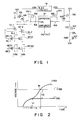
- Fig. 1 illustrates the data-reading section of a known nonvolatile semiconductor memory (EPROM) of single-bit line output type.
- the memory cell array 11 of the EPROM comprises memory cells MC11, MC12, ... MC21, MC22, ... which comprise each a floating-gate MOSFET and which are arranged in rows and columns.
- the drains of the memory cells MC of each column are connected to a bit line (BL1, BL2, ).
- the source of every memory cell MC is connected to the ground Vss.
- the control gates of the cells MC of each row are connected to a word line (WL1, WC2, ).
- the word lines WL1, WL2, ... are connected to a row decoder (not shown), thereby to receive the signals output from the row decoder.
- the memory cell array further comprises a Y selector having N-channel MOS transistors 12-1, 12-2, The current paths of these MOS transistors are connected at one end to the bit lines BL1, BL2, ..., and at the other end to each other.
- the gates of the MOS transistors 12-1, 12-2, ... are connected to a column decoder (not shown) to receive the signals output from the column decoder.
- the cell array also has an N-channel charging MOS transistor 13A, an N-channel clamping MOS transistor 14A, a sense line 15A, and a P-channel load MOS transistor 16A.
- the current path of the charging MOS transistor 13A is connected between a power supply Vcc and the node of the MOS transistors 12-1, 12-2, ... of the Y selector.
- the current path of the clamping MOS transistor 14A is connected the node of the MOS transistors 12-1, 12-2, ... and one end of the sense line 15A.
- the current path of the P-channel load MOS transistor 16A is connected between the sense line 15A and the power supply Vcc.
- the gate of the MOS transistor 16A is connected to the sense line 15A.
- the EPROM further comprises a dummy cell DMC, a dummy bit line DBL, an N-channel MOS transistor 12D, an N-channel charging MOS transistor 13B, an N-channel clamping MOS transistor 14B, a reference line 15B, and a P-channel load MOS transistor 16B.
- the source and control gate of the dummy cell DMC are connected to the ground Vss and the power supply Vcc, respectively.
- the dummy cell DMC is of the same size as the memory cells MC as in the case of most nonvolatile semiconductor memories.
- the drain of the dummy cell DMC is connected by the dummy bit line DBL to the source of the N-channel MOS transistor 12D which has the same size as the MOS transistors 12-1, 12-2 ... of the Y selector.
- the gate of the MOS transistor 12D is connected to the power supply Vcc.
- the current path is the charging MOS transistor 13B is connected between the drain of the MOS transistor 12D and the power supply Vcc.
- the current path of the N-channel clamping MOS transistor 14B is coupled between the drain of the MOS transistor 12D and one end of the reference line 15B.
- the current path of the load MOS transistor 16B is connected between the reference line 15B and the power supply Vcc.
- the gate of the load MOS transistor 16B is connected to the reference line 15B.
- the load MOS transistor 16B has a conductance greater than that of the load MOS transistor 16A, whereby a potential difference is present between the sense line 15A and the reference line 15B.
- the EPROM further comprises a differential amplifier 17 and a bias circuit 18.
- the bias circuit 18 applies a bias voltage Vbb to the gates of the MOS transistors 13A, 14A, 13B, and 14B, thereby to suppress the writing errors which would otherwise likely to occur while data is being read from the EPROM.
- Vbb bias voltage
- the differential amplifier 17 has two inputs, which are connected to the other end of the sense line 15A and the other end of the reference line 15B, respectively.
- the differential amplifier 17 amplifies the difference between the potential of the sense line 15A and that of the reference line 15B, and produces an output representing this potential difference.
- the potential of the sense line 15A is the voltage which the load MOS transistor 16A has converted from the conductance of any memory cell MC selected.
- the potential of the reference line 15B is the voltage which the load MOS transistor 16B has converted from the conductance of the dummy cell DMC.
- the output of the amplifier 17 is proportional to the difference between the conductance of any selected memory cell MC and that of the dummy cell DMC.
- Each memory cell MC stores a "0" bit if it has a cell current Imc of 0 ⁇ A, or a "1" bit if it has a cell current Imc of 100 ⁇ A. If any selected memory cell MC stores a "1" bit -- that is, if electrons have been injected into the floating gate of the memory cell MC, the threshold voltage of the memory cell MC is high, and the conductance thereof is also high. In this case, the potential of the sense line 15A is higher than that of the reference line 15B. If the selected memory cell MC stores a "0" bit -- that is, if no electrons have been injected into the floating gate of the memory cell MC, the threshold voltage of the cell MC is low, and the conductance thereof is also low. In this case, the potential of the sense line 15A is lower than that of the reference line 15B. In either case, the differential amplifier 17 amplifies the difference between the potentials of the lines 15A and 15B, thereby reading data from the selected memory MC.
- the access speed of the circuit shown in Fig. 1 greatly depend on the time required to read data from a memory cell MC storing a "0" bit after data has been read from a memory cell MC connected to the same word line WL and storing a "1" bit.
- the "1" bit is read from the selected memory cell in the following manner. First, the word line WL, to which the target memory cell MC storing a "1" bit, is connected is selected. Then, a potential is applied to this word line WL. Next, the bit line BL to which the target memory cell MC is discharged to the ground potential, whereby the "1" bit is read from the memory cell MC.
- Fig. 2 is a graph representing how the potentials of the bit line BL, the sense line 15A and the reference line 15B change with time.
- the potential VBL of the bit line BL increases for time t1, from 0 V to the value V1 determined by the bias voltage Vbb applied from the bias circuit 18, and remains at this value Vl thereafter.
- the potential V15A of the sense line 15A increases in the same way as the potential VBL, for a period of time tl, and keeps increasing thereafter since it is not clamped by the bias voltage Vbb.
- the potential V15A reaches the potential V15B of the reference line 15B.
- the delay time t1 and the delay time t2 are determined mostly by CV/i, where C is parasitic capacitance, V is a potential difference, and i is a current.
- the capacitance C which determines the delay time t1 is in turn determined by the parasitic capacitance of the bit line BL, the parasitic capacitance present between the semiconductor substrate and the drain region of the selecting MOS transistor 12, and the parasitic capacitance coupled to that input node of the amplifier 17 which is connected to the sense line 15A.
- the current i which is another determinant of the delay time time t1 is the sum of the current i1 supplied from the load MOS transistor 16A and the current i2 supplied from the charging MOS transistor 13A.
- the potential difference V i.e., the third determinant of the delay time t1, is the difference V1 between the ground potential and the potential VBL of the bit line BL.
- the parasitic capacitance of the bit line BL and that of the selecting MOS transistor 12 tend to increase in proportion to the storage capacity of the EPROM.
- the current i1 supplied from the load MOS transistor 16A is determined by the conductance of the memory cells MC, and therefore decreases in inverse proportion to the size of the memory cells MC.
- the parasitic capacitance determining the delay time t2 is, in turn, determined by four determinants. These determinants are: the parasitic capacitance present between the semiconductor substrate and the gate electrode of the load MOS transistor 16A; the parasitic capacitance present between the semiconductor substrate and the drain region of the transistor 16A; the input capacitance of the differential amplifier 17; and the parasitic capacitance present between the semiconductor substrate and the drain region of the clamping MOS transistor 14A.
- the current i which is the second determinant of the delay time t2, is the current i1 flowing the current path of the load MOS transistor 14A.
- the object of the present invention is to provide a semiconductor memory device of single-bit line output type, from which data can be read at high speed.
- a semiconductor memory device comprises a memory-cell array having memory cells of single-bit output type, arranged in rows and columns, and a plurality of selecting bipolar transistors having emitters coupled to the drains of the memory cells, collectors connected to one another, and bases connected to receive select signals, whereby data stored in the memory cells can be read from the node of the collectors of the bipolar transistors.
- Each bit line of the semiconductor memory device is precharged with the currents flowing, respectively, in the collector-emitter path and base-emitter path of the selecting bipolar transistor connected to the bit line.
- the bit line can be precharged at high speed, making it possible to read data from each memory cell at high speed.
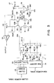
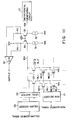
- Fig. 3 illustrates a semiconductor memory according to a first embodiment of the invention.
- the memory cell array 11 of this device comprises memory cells MC11, MC12, ..., MC21, MC22, ..., which are floating-gate MOSFETs and arranged in rows and columns, the drains of the memory cells MC of each column are coupled to a bit line BL, and the sources of these memory cells MC are connected to the ground Vss.
- the control gates of the memory cells MC of each row are connected to a word line WL.
- the word lines WL1, WL2, are connected to a row decoder 21 to receive the decoded row-address signals from the row decoder 21.
- the semiconductor memory has a Y selector which has NPN transistors 22-1, 22-2, ...
- the emitters of the transistors 22-1, 22-2, ... are connected bit lines BL1, BL2, ..., and the collectors thereof are connected to one end of a sense line 15A.
- the base of the NPN transistors 22-1, 22-2, ... are connected to a column decoder 23 to receive decoded column-address signals supplied from the decoder 23 through a level shifter 24.
- the level shifter 24 changes the decoded column-address signals at CMOS logic levels, which have been output from the column decoder 23.
- the shifter 24 changes a logic "1" level (i.e., power-supply potential Vcc) to a potential Vba of, for example, 2 V which is somewhere between the power-supply potential Vcc and the ground potential Vss, and changes a logic "0" level (i.e., the ground potential Vss) to 0 V.
- the logic "1" level is shifted to the potential Vba in order to prevent soft errors from occurring when the drain voltages of the memory cells MC are excessively high.
- Row-address signals are input the row decoder 21, and are decoded thereby.
- Column-address signals are input to the column decoder 23, and are decoded thereby.
- the semiconductor memory has a dummy cell DMC having a source connected to the ground Vss and a control gate applied with the power-supply potential Vcc.
- the dummy cell DMC has the same size as the memory cells MC.
- the drain of the dummy cell DMC is connected by a dummy bit line DBL to the emitters of NPN transistors 25 and 26.
- the collectors of the NPN transistors 25 and 26 are coupled to one end of the sense line 15A.
- the bases of the NPN transistors 25 and 26 are connected to each other.
- a bias voltage Vba is applied to the bases of these transistors 25 and 26.
- the bias voltage Vba is substantially equal to the voltage applied to the bases of the selecting NPN transistors 22-1, 22-2, ... to select these transistors 22-1, 22-2, ...
- the dummy cell DMC and the NPN transistors 25 and 26 constitute a circuit 27, which generates and applies a reference potential V15B to
- NPN transistors 25 and 26 have the same emitter area.
- a current Imc is supplied to the sense line 15A from the emitter of a transistor 29, and a current Idc is supplied to the reference line 15B from the emitter of a transistor 30.
- a current of Imc/2 flows in the collector-emitter path of the transistor 25; a current of Imc/2 flows in the collector-emitter path of the transistor 26; and a current of Imc flows in the drain-source path of the dummy cell DMC.
- the semiconductor memory further comprises a current-sensing amplifier 28 having two inputs, which are coupled to the other end of the sense line 15A and the other end of the reference line 15B.
- the amplifier 28 comprises the NPN transistors 29 and 30, a load resistors R1 and R2, and constant current sources 31 and 32.
- the emitters of the NPN transistors 29 and 30 are coupled to the other ends of the lines 15A and 15B, respectively.
- the bias voltage Vbb is applied to the bases of the NPN transistors 29 and 30.
- the current source 31 is connected between the emitter of the NPN transistor 29 and the ground Vss
- the current source 32 is connected between the emitter of the NPN transistor 30 and the ground Vss.
- the load resistor R1 is coupled between the collector of the NPN transistor 29 and the power supply Vcc, and the load resistor R2 is connected between the collector of the NPN transistor 30 and the power supply Vcc.
- the emitters of the transistors 29 and 30 serve as input nodes of the amplifier 28, whereas the collectors of the transistors 29 and 30 function as output nodes of the amplifier 28.
- the two output signals Vout1 and Vout2 supplied from the current-sensing amplifier 28 are input to a differential amplifier 33.
- the amplifier 33 compares the signals Vout1 and Vout2 and amplifies the difference between these input signals, thereby reading the CMOS logic level of the data stored in any memory cell MC selected.
- Fig. 4 shows the differential amplifier 33.
- the amplifier 33 comprises two P-channel MOS transistors 34 and 35 and a current mirror circuit 38 constituted by two N-channel MOS transistors 36 and 37.
- the gates of the P-channel MOS transistors 34 and 35 are connected to the outputs of the current-sensing amplifier 28 to receive the output signals Vout1 and Vout2.
- the sources of the MOS transistors 34 and 35 are connected to the power supply Vcc.
- the drains of the MOS transistors 34 and 35 are connected to the ground Vss, thus forming two nodes.
- the current mirror circuit 38 is connected between these nodes.
- a signal at a CMOS logic level is output from the node of the MOS transistors 34 and 36.
- a potential Vba is applied to the base of one of the selecting NPN transistors 22-1, 22-2, ...
- this potential Vba is 0 V
- no memory cells MC, coupled to the bit line BL to which the selecting NPN transistor is coupled are selected.
- the potential is about 2 V
- the memory cells MC coupled to the bit line BL are selected.
- the bit line BL is clamped at a potential which is at most, 1.3 V or (2 - Vf)V, where Vf is the base-emitter voltage of the NPN transistors 22-1, 22-2, ...
- the bit line BL is charged from 0 V to 1.3 V as the base potential of the selected NPN transistor 22 increases from 0 V to 2 V.
- the charging current ie is the sum of the collector current ic and base current ib of the transistor 22.
- the collector current ic which is determined by the conductance of the memory cells MC, is approximately (i1 + i2) as in the conventional semiconductor memory.
- the bit line BL can be quickly charged, nevertheless, from 0 V to 1.3 V.
- the potential V15A of the sense line 15A changes.
- the potential V15A is defined, as follows, by the parameters of the current-sensing amplifier 28: where io is the saturated current of a diode, and kT/q is a voltage which is about 25 mV at room temperature.
- the current Ibs supplied from the constant current sources 31 and 32 is substantially the same as the current Imc flowing via the sense line 15A.
- the time delay of the amplifier 33 is far shorter than the delay time t1 or t2, because the potential difference which the amplifier 33 amplifies to 5 V is as high as 0.5 V to 1 V, not a few millivolts as in the case of the circuit shown in Fig. 1.
- Vout1 Vcc - R1 (Ibs + Imc)
- Vout2 Vcc - R2 (Ibs + Imc)
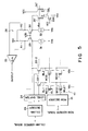
- the circuit 27 may be modified as is illustrated in Fig. 5.
- K can be set to any desired value.
- This circuit either comprises NPN transistors 25′ and 26′ having emitters of different sizes m and n, or m emitters and n emitters, respectively all emitters having the same size.
- the emitter currents for the "0"-side and the "1"-side area (Se is the area of each emitter of the multi-emitter transistors 25′ and 26′), pro vided that the base-emitter currents for the "0"-side and the "1"-side are identical.
- an NPN bipolar transistor is larger than a MOS transistor.
- the selecting NPN transistors 22-1, 22-2, ... may not be arranged at so short intervals as the memory cells MC, which are MOS transistors. If this is the case, the memory-cell array 11 can be divided into blocks 11-1, 11-2, ... as is illustrated in Fig. 6, and the NPN transistors 22-1, 22-2, ... can be provided for these cell-array blocks 11-1, 11-2, ... respectively. More specifically, the sources of N-channel MOS transistors 39-1, 39-2, ... are connected to bit lines BL1, BL2, ..., and the drains of the N-channel MOS transistors of each block are connected to one another.
- the node of the drains of the N-channel MOS transistors of the first block is coupled to the emitter of the NPN transistor 22-1; the node of the drains of the N-channel MOS transistors of the second block is connected to the emitter of the NPN transistor 22-2; and so forth.
- the collectors of the transistors 22-1, 22-2, ... are connected to a sense line 15A.
- the gates of the N-channel MOS transistors 39-1, 39-2, ... of each cell-array block are connected to a column decoder 23, so that the memory cells MC of the columns corresponding to the N-channel MOS transistors 39-1, 39-2, ...
- the bases of the NPN transistors 22-1, 22-2, ... are connected to a level shifter 23 to receive the signals output from the level shifter 24.
- the level shifter 24 is connected to the column decoder 23 to receive the upper bits output from the decoder 23.
- the semiconductor memory shown in Fig. 6 operates in the following way.
- any PNP transistor 22 is selected, it in turn selects the corresponding cell-array block.
- the MOS transistors 39-1, 39-2 , ... of provided for this cell-array block therefore select the columns of memory cells MC of the selected block.
- the MOS transistors 39-1, 39-2 are controlled directly by the upper bits of the decoded column address supplied from the column decoder 23, which are signals at 0 V to 5 V. Nevertheless, the potentials of the bit lines BL are clamped at approximately 1.2 V. This is because the base potentials of the NPN transistors 22-1, 22-2, ... are not higher than about 2 V.
- the NPN transistors 22-1, 22-2, ... for the cell-array blocks 11-1, 11-2, ..., respectively. Since only one NPN transistor is connected to the plural bit lines BL used in each cell-array block, the NPN transistors 22 can be arranged at so short intervals as the memory cells MC.
- Fig. 7 is a circuit diagram schematically illustrating the data-reading section of a memory device according to a fourth embodiment of the invention.
- This memory device is identical to the device shown in Fig. 5, except that two diodes D1 and D2 are connected in parallel to a resistor R1, and two diodes D3 and D4 are connected in parallel to a resistor R2.
- the diodes D1 and D2 are connected in the forward direction with respect to the power-supply Vcc.
- the diodes D3 and D4 are connected also in the forward direction with respect to the power supply Vcc.
- the current which charges the bit lines BL, flows not only through the resistor R1, but also through the diodes D1 and D2.
- the current which charges the dummy bit line DBL, flows not only through the resistor R2, but also through the diodes D3 and D4.
- the potential difference between the sense line 15A and the reference line 15B can be detected within a time shorter than in the memory device illustrated in Fig. 5.
- Fig. 8 schematically illustrates the data-reading section of a memory device according to a fifth embodiment of the invention.
- This memory device has a current-sensing amplifier which is suitable for the case where the bit-line capacitance is large, and the capacitance of each collector dotting node is also large.
- This current-sensing amplifier comprises two current-sensing units 40-1 and 40-2 connected to the memory cell array 11 and one current-sensing unit 41 coupled the circuit 27 for generating a reference potential.
- the outputs of these current-sensing units 40-1, 40-2, and 42 are multiplexed by means of an ECL gate 42.
- the output of this gate 42 is amplified by the differential amplifier 33.
- a selector 45-1 comprised of an NPN transistor 43-1 and a constant current source 44-1 is connected to the current-sensing unit 40-1.
- a selector 45-2 constituted by an NPN transistor 43-2 and a constant current source 44-2 is connected to the current-sensing unit 40-2.
- the ECL gate 42 includes NPN transistors 46-1 to 46-3, load resistors R3 and R4, and a constant current source 47.
- the base of the NPN transistor 46-1 is connected to the collector of the NPN transistor 29-1.
- the base of the NPN transistor 46-2 is coupled to the collector of the NPN transistor 29-2.
- the base of the NPN transistor 46-3 is coupled to the collector of the NPN transistor 30.
- the resistor R3 is coupled between the power supply Vcc and the node of the collectors of the NPN transistors 46-1 and 46-2.
- the resistor R4 is connected between the power supply Vcc and the collector of the NPN transistor 27.
- the emitters of the NPN transistors 46-1 and 46-2 are connected to each other.
- the constant current source 47 is coupled between the ground Vss and the node of the emitters of the NPN transistors 46-1 and 46-2.
- the node of the collectors of the NPN transistors 46-1 and 46-2 is connected to one of the two input nodes of a differential amplifier 33.
- the collector of the NPN transistor 46-3 is coupled to the other input node of the differential amplifier 33.
- the current-sensing unit 40-1 When a select signal SS1 is at an "L” level, and a select signal SS2 is at a "H” level, the current-sensing unit 40-1 is selected.
- the collector potential of the NPN transistor 29-1 is either at the "H” level or the logic “L” level, in accordance with the data stored in any selected memory cell of the cell-array block 11-1 connected to the emitter of the NPN transistor 29-1.
- the collector of the NPN transistor 29-2 is at the "1" level, whatever data is stored in any selected memory cell of the cell-array block 11-2 connected to the emitter of the NPN transistor 29-2.
- the collector potential of the NPN transistor 30 is determined by the output potential of the circuit 27. The difference between the base potentials of the transistors 46-3 and 46-1 determines the output of the differential amplifier 33.
- the current-sensing unit 40-2 is selected.
- the data is read from any selected memory cell of the cell-array block 11-2, imposing no influence on the data stored in the cell-array block 11-1.
- the present invention is not limited to the embodiments described above, which are of the single end type. Nevertheless, this invention can be applied to such an architecture as is shown in Fig. 9, wherein two memory-cell arrays 11A and 11b are coupled to the input nodes of a current-sensing amplifier 28 by means of sense lines 15A and 15B.
- this architecture different data items are written into the corresponding cells of the arrays 11A and 11B. To read this data, the corresponding cells are selected, and the difference between the potentials of the sense lines 15A and 15B is amplified first by the current-sensing amplifier 28 and then by a differential amplifier 33.
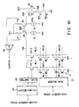
- the memory cells of the embodiments described above are EPROM cells. However, the can be EEPROM cells as is shown in Fig. 10, mask ROM cells as is illustrated in Fig. 11, or ROM cells with NAND-cell structure as is illustrated in Fig. 12.
- the circuits shown in Figs. 10, 11, and 12 are identical in both structure and operation to the embodiments described above, except for the types of the memory cells employed. Therefore, neither their structures nor their operations will not be described or explained.
Landscapes
- Read Only Memory (AREA)
- Static Random-Access Memory (AREA)
Applications Claiming Priority (2)
| Application Number | Priority Date | Filing Date | Title |
|---|---|---|---|
| JP10529189A JP2601903B2 (ja) | 1989-04-25 | 1989-04-25 | 半導体記憶装置 |
| JP105291/89 | 1989-04-25 |
Publications (3)
| Publication Number | Publication Date |
|---|---|
| EP0398048A2 true EP0398048A2 (de) | 1990-11-22 |
| EP0398048A3 EP0398048A3 (de) | 1993-08-25 |
| EP0398048B1 EP0398048B1 (de) | 1995-09-20 |
Family
ID=14403582
Family Applications (1)
| Application Number | Title | Priority Date | Filing Date |
|---|---|---|---|
| EP90107869A Expired - Lifetime EP0398048B1 (de) | 1989-04-25 | 1990-04-25 | Halbleiterspeichereinrichtung mit hoher Datenlesegeschwindigkeit |
Country Status (5)
| Country | Link |
|---|---|
| US (1) | US5371703A (de) |
| EP (1) | EP0398048B1 (de) |
| JP (1) | JP2601903B2 (de) |
| KR (1) | KR930000813B1 (de) |
| DE (1) | DE69022475T2 (de) |
Cited By (2)
| Publication number | Priority date | Publication date | Assignee | Title |
|---|---|---|---|---|
| EP0463378A3 (en) * | 1990-06-29 | 1994-07-27 | Texas Instruments Inc | An electrically-erasable, electrically-programmable read-only memory cell with a selectable threshold voltage and methods for its use |
| EP1071096A1 (de) * | 1999-07-22 | 2001-01-24 | STMicroelectronics S.r.l. | Leseschaltung für einen nichtflüchtigen Speicher |
Families Citing this family (14)
| Publication number | Priority date | Publication date | Assignee | Title |
|---|---|---|---|---|
| KR960008456B1 (en) * | 1993-10-06 | 1996-06-26 | Hyundai Electronics Ind | Sense amplifier of semiconductor memory device |
| US5608679A (en) * | 1994-06-02 | 1997-03-04 | Intel Corporation | Fast internal reference cell trimming for flash EEPROM memory |
| JPH08180697A (ja) * | 1994-09-16 | 1996-07-12 | Texas Instr Inc <Ti> | センス増幅器用の基準電流を供給する基準回路及び方法 |
| US5896315A (en) * | 1997-04-11 | 1999-04-20 | Programmable Silicon Solutions | Nonvolatile memory |
| KR100326236B1 (ko) | 1998-12-30 | 2002-05-09 | 박종섭 | 모스/바이폴라복합트랜지스터를이용한반도체메모리장치의감지증폭기 |
| JP2004335031A (ja) * | 2003-05-09 | 2004-11-25 | Toshiba Corp | 半導体記憶装置 |
| JP2004355783A (ja) * | 2003-05-30 | 2004-12-16 | Sharp Corp | 光情報記録媒体とその再生方法 |
| JP2006260742A (ja) * | 2005-02-15 | 2006-09-28 | Sanyo Electric Co Ltd | メモリ |
| JP2006331620A (ja) * | 2005-04-28 | 2006-12-07 | Toshiba Corp | 半導体集積回路 |
| US8547756B2 (en) | 2010-10-04 | 2013-10-01 | Zeno Semiconductor, Inc. | Semiconductor memory device having an electrically floating body transistor |
| US8130547B2 (en) * | 2007-11-29 | 2012-03-06 | Zeno Semiconductor, Inc. | Method of maintaining the state of semiconductor memory having electrically floating body transistor |
| US7542348B1 (en) * | 2007-12-19 | 2009-06-02 | Juhan Kim | NOR flash memory including bipolar segment read circuit |
| US10340276B2 (en) | 2010-03-02 | 2019-07-02 | Zeno Semiconductor, Inc. | Method of maintaining the state of semiconductor memory having electrically floating body transistor |
| US8638605B2 (en) | 2011-05-25 | 2014-01-28 | Micron Technology, Inc. | Apparatus and methods including a bipolar junction transistor coupled to a string of memory cells |
Family Cites Families (27)
| Publication number | Priority date | Publication date | Assignee | Title |
|---|---|---|---|---|
| US4237472A (en) * | 1979-03-12 | 1980-12-02 | Rca Corporation | High performance electrically alterable read only memory (EAROM) |
| JPS59914B2 (ja) * | 1979-08-23 | 1984-01-09 | 富士通株式会社 | 半導体記憶装置 |
| US4301518A (en) * | 1979-11-01 | 1981-11-17 | Texas Instruments Incorporated | Differential sensing of single ended memory array |
| GB2089612B (en) * | 1980-12-12 | 1984-08-30 | Tokyo Shibaura Electric Co | Nonvolatile semiconductor memory device |
| JPS5885638A (ja) * | 1981-11-17 | 1983-05-23 | Ricoh Co Ltd | プログラマブルロジツクアレイ |
| JPH0648595B2 (ja) * | 1982-08-20 | 1994-06-22 | 株式会社東芝 | 半導体記憶装置のセンスアンプ |
| JPS5968889A (ja) * | 1982-10-08 | 1984-04-18 | Toshiba Corp | 半導体記憶装置 |
| US4604533A (en) * | 1982-12-28 | 1986-08-05 | Tokyo Shibaura Denki Kabushiki Kaisha | Sense amplifier |
| JPS59218696A (ja) * | 1983-05-26 | 1984-12-08 | Toshiba Corp | 半導体メモリ |
| JPH0666115B2 (ja) * | 1983-09-26 | 1994-08-24 | 株式会社東芝 | 半導体記憶装置 |
| JPH0654598B2 (ja) * | 1985-03-27 | 1994-07-20 | 株式会社日立製作所 | 半導体メモリ |
| EP0179351B1 (de) * | 1984-10-11 | 1992-10-07 | Hitachi, Ltd. | Halbleiterspeicher |
| US4663741A (en) * | 1984-10-16 | 1987-05-05 | Trilogy Systems Corporation | Strobed access semiconductor memory system |
| US4654831A (en) * | 1985-04-11 | 1987-03-31 | Advanced Micro Devices, Inc. | High speed CMOS current sense amplifier |
| JPS60237698A (ja) * | 1985-04-23 | 1985-11-26 | Hitachi Ltd | 半導体回路 |
| JPS62117190A (ja) * | 1985-11-15 | 1987-05-28 | Hitachi Ltd | 半導体記憶装置 |
| JPS62175997A (ja) * | 1986-01-29 | 1987-08-01 | Hitachi Ltd | 半導体不揮発性記憶装置 |
| JPS62229600A (ja) * | 1986-03-31 | 1987-10-08 | Toshiba Corp | 不揮発性半導体記憶装置 |
| US4821235A (en) * | 1986-04-17 | 1989-04-11 | Fairchild Semiconductor Corporation | Translinear static memory cell with bipolar and MOS devices |
| EP0523756A3 (en) * | 1986-08-15 | 1993-06-09 | Nec Corporation | Static random access memory having bi-cmos construction |
| JPS6381685A (ja) * | 1986-09-26 | 1988-04-12 | Hitachi Ltd | 半導体記憶装置 |
| US4849933A (en) * | 1987-05-06 | 1989-07-18 | Advanced Micro Devices, Inc. | Bipolar programmable logic array |
| US4858183A (en) * | 1987-06-02 | 1989-08-15 | Texas Instruments Incorporated | ECL high speed semiconductor memory and method of accessing stored information therein |
| JP2585602B2 (ja) * | 1987-06-10 | 1997-02-26 | 株式会社日立製作所 | 半導体記憶装置 |
| JPS6415960A (en) * | 1987-07-10 | 1989-01-19 | Hitachi Ltd | Assembly equipment |
| JPH0682520B2 (ja) * | 1987-07-31 | 1994-10-19 | 株式会社東芝 | 半導体メモリ |
| JP2537264B2 (ja) * | 1988-04-13 | 1996-09-25 | 株式会社東芝 | 半導体記憶装置 |
-
1989
- 1989-04-25 JP JP10529189A patent/JP2601903B2/ja not_active Expired - Fee Related
-
1990
- 1990-04-25 DE DE69022475T patent/DE69022475T2/de not_active Expired - Fee Related
- 1990-04-25 KR KR1019900005817A patent/KR930000813B1/ko not_active Expired - Fee Related
- 1990-04-25 EP EP90107869A patent/EP0398048B1/de not_active Expired - Lifetime
-
1993
- 1993-07-21 US US08/094,359 patent/US5371703A/en not_active Expired - Lifetime
Cited By (3)
| Publication number | Priority date | Publication date | Assignee | Title |
|---|---|---|---|---|
| EP0463378A3 (en) * | 1990-06-29 | 1994-07-27 | Texas Instruments Inc | An electrically-erasable, electrically-programmable read-only memory cell with a selectable threshold voltage and methods for its use |
| EP1071096A1 (de) * | 1999-07-22 | 2001-01-24 | STMicroelectronics S.r.l. | Leseschaltung für einen nichtflüchtigen Speicher |
| US6327184B1 (en) | 1999-07-22 | 2001-12-04 | Stmicroelectronics S.R.L. | Read circuit for a nonvolatile memory |
Also Published As
| Publication number | Publication date |
|---|---|
| EP0398048A3 (de) | 1993-08-25 |
| EP0398048B1 (de) | 1995-09-20 |
| KR900017037A (ko) | 1990-11-15 |
| JP2601903B2 (ja) | 1997-04-23 |
| US5371703A (en) | 1994-12-06 |
| JPH02282995A (ja) | 1990-11-20 |
| DE69022475D1 (de) | 1995-10-26 |
| DE69022475T2 (de) | 1996-03-21 |
| KR930000813B1 (ko) | 1993-02-05 |
Similar Documents
| Publication | Publication Date | Title |
|---|---|---|
| US5371713A (en) | Semiconductor integrated circuit | |
| US5321655A (en) | Semiconductor memory device | |
| US5197028A (en) | Semiconductor memory device with dual reference elements | |
| US5608676A (en) | Current limited current reference for non-volatile memory sensing | |
| EP0398048A2 (de) | Halbleiterspeichereinrichtung mit hoher Datenlesegeschwindigkeit | |
| US4933906A (en) | Non-volatile semiconductor memory device | |
| US5163022A (en) | Semiconductor cell memory with current sensing | |
| KR950001289B1 (ko) | 반도체기억장치 | |
| US7072236B2 (en) | Semiconductor memory device with pre-sense circuits and a differential sense amplifier | |
| US4962482A (en) | Nonvolatile memory device using a sense circuit including variable threshold transistors | |
| US5229968A (en) | Nonvolatile semiconductor memory wherein dummy cells are used for generating a potential for detecting data | |
| EP1226586B1 (de) | Wortleitungssignale einer flashspeicher bleiben überall auf dem chip verlustfrei | |
| EP0179351A2 (de) | Halbleiterspeicher | |
| US5528544A (en) | Semiconductor memory device having high speed sense amplifier | |
| KR900004327B1 (ko) | 센스증폭기와 프로그래밍회로 각각에 독립으로 칼럼 트랜지스터 게이트 트랜스터 그룹을 갖게한 반도체 기억장치 | |
| US6141277A (en) | Semiconductor memory preventing sense amplifier malfunctions due to effects of noise generated in output buffer | |
| US5040143A (en) | Semiconductor memory device | |
| US4435789A (en) | Circuit for a read-only memory organized in rows and columns to prevent bit line potentials from dropping | |
| US5199000A (en) | Semiconductor memory circuit having switched voltage supply for data bus lines | |
| KR960002737B1 (ko) | 비휘발성 메모리장치용 기입회로 | |
| US5825687A (en) | Low voltage memory cell, circuit array formed thereby and method of operation therefor | |
| JP3581207B2 (ja) | 不揮発性半導体メモリ | |
| KR950002728B1 (ko) | 판독 전용 메모리 디바이스 | |
| JPH0782758B2 (ja) | 半導体記憶装置 | |
| EP0429018A2 (de) | Halbleiterspeicheranordnung mit Eingangs-/Ausgangs-Datensignalleitungen, die Bitinformation in Hochgeschwindigkeit übertragen unabhängig von der Schwankung des Speisespannungssignals |
Legal Events
| Date | Code | Title | Description |
|---|---|---|---|
| PUAI | Public reference made under article 153(3) epc to a published international application that has entered the european phase |
Free format text: ORIGINAL CODE: 0009012 |
|
| 17P | Request for examination filed |
Effective date: 19900425 |
|
| AK | Designated contracting states |
Kind code of ref document: A2 Designated state(s): DE FR GB |
|
| PUAL | Search report despatched |
Free format text: ORIGINAL CODE: 0009013 |
|
| AK | Designated contracting states |
Kind code of ref document: A3 Designated state(s): DE FR GB |
|
| 17Q | First examination report despatched |
Effective date: 19940520 |
|
| GRAA | (expected) grant |
Free format text: ORIGINAL CODE: 0009210 |
|
| AK | Designated contracting states |
Kind code of ref document: B1 Designated state(s): DE FR GB |
|
| REF | Corresponds to: |
Ref document number: 69022475 Country of ref document: DE Date of ref document: 19951026 |
|
| ET | Fr: translation filed | ||
| PLBE | No opposition filed within time limit |
Free format text: ORIGINAL CODE: 0009261 |
|
| STAA | Information on the status of an ep patent application or granted ep patent |
Free format text: STATUS: NO OPPOSITION FILED WITHIN TIME LIMIT |
|
| 26N | No opposition filed | ||
| PGFP | Annual fee paid to national office [announced via postgrant information from national office to epo] |
Ref country code: FR Payment date: 19970409 Year of fee payment: 8 |
|
| PGFP | Annual fee paid to national office [announced via postgrant information from national office to epo] |
Ref country code: DE Payment date: 19970505 Year of fee payment: 8 |
|
| PG25 | Lapsed in a contracting state [announced via postgrant information from national office to epo] |
Ref country code: FR Free format text: THE PATENT HAS BEEN ANNULLED BY A DECISION OF A NATIONAL AUTHORITY Effective date: 19980430 |
|
| REG | Reference to a national code |
Ref country code: GB Ref legal event code: 746 Effective date: 19981010 |
|
| PG25 | Lapsed in a contracting state [announced via postgrant information from national office to epo] |
Ref country code: DE Free format text: LAPSE BECAUSE OF NON-PAYMENT OF DUE FEES Effective date: 19990202 |
|
| REG | Reference to a national code |
Ref country code: FR Ref legal event code: ST |
|
| REG | Reference to a national code |
Ref country code: GB Ref legal event code: IF02 |
|
| PGFP | Annual fee paid to national office [announced via postgrant information from national office to epo] |
Ref country code: GB Payment date: 20060419 Year of fee payment: 17 |
|
| GBPC | Gb: european patent ceased through non-payment of renewal fee |
Effective date: 20070425 |
|
| PG25 | Lapsed in a contracting state [announced via postgrant information from national office to epo] |
Ref country code: GB Free format text: LAPSE BECAUSE OF NON-PAYMENT OF DUE FEES Effective date: 20070425 |