EP0259942A2 - Piezoelektrischer Druckfühler für Prüfstationen für integrierte Schaltungen - Google Patents
Piezoelektrischer Druckfühler für Prüfstationen für integrierte Schaltungen Download PDFInfo
- Publication number
- EP0259942A2 EP0259942A2 EP87302425A EP87302425A EP0259942A2 EP 0259942 A2 EP0259942 A2 EP 0259942A2 EP 87302425 A EP87302425 A EP 87302425A EP 87302425 A EP87302425 A EP 87302425A EP 0259942 A2 EP0259942 A2 EP 0259942A2
- Authority
- EP
- European Patent Office
- Prior art keywords
- probe
- piezoelectric element
- sensing apparatus
- pressure
- pressure pad
- Prior art date
- Legal status (The legal status is an assumption and is not a legal conclusion. Google has not performed a legal analysis and makes no representation as to the accuracy of the status listed.)
- Withdrawn
Links
Images
Classifications
-
- G—PHYSICS
- G01—MEASURING; TESTING
- G01R—MEASURING ELECTRIC VARIABLES; MEASURING MAGNETIC VARIABLES
- G01R31/00—Arrangements for testing electric properties; Arrangements for locating electric faults; Arrangements for electrical testing characterised by what is being tested not provided for elsewhere
- G01R31/28—Testing of electronic circuits, e.g. by signal tracer
- G01R31/2851—Testing of integrated circuits [IC]
- G01R31/2886—Features relating to contacting the IC under test, e.g. probe heads; chucks
-
- G—PHYSICS
- G01—MEASURING; TESTING
- G01L—MEASURING FORCE, STRESS, TORQUE, WORK, MECHANICAL POWER, MECHANICAL EFFICIENCY, OR FLUID PRESSURE
- G01L1/00—Measuring force or stress, in general
- G01L1/16—Measuring force or stress, in general using properties of piezoelectric devices
-
- G—PHYSICS
- G01—MEASURING; TESTING
- G01R—MEASURING ELECTRIC VARIABLES; MEASURING MAGNETIC VARIABLES
- G01R1/00—Details of instruments or arrangements of the types included in groups G01R5/00 - G01R13/00 and G01R31/00
- G01R1/02—General constructional details
- G01R1/06—Measuring leads; Measuring probes
- G01R1/067—Measuring probes
- G01R1/06794—Devices for sensing when probes are in contact, or in position to contact, with measured object
-
- G—PHYSICS
- G01—MEASURING; TESTING
- G01R—MEASURING ELECTRIC VARIABLES; MEASURING MAGNETIC VARIABLES
- G01R1/00—Details of instruments or arrangements of the types included in groups G01R5/00 - G01R13/00 and G01R31/00
- G01R1/02—General constructional details
- G01R1/06—Measuring leads; Measuring probes
- G01R1/067—Measuring probes
- G01R1/073—Multiple probes
- G01R1/07307—Multiple probes with individual probe elements, e.g. needles, cantilever beams or bump contacts, fixed in relation to each other, e.g. bed of nails fixture or probe card
- G01R1/0735—Multiple probes with individual probe elements, e.g. needles, cantilever beams or bump contacts, fixed in relation to each other, e.g. bed of nails fixture or probe card arranged on a flexible frame or film
Definitions
- the present invention generally relates to probe systems used in integrated circuit testing stations, and more particularly to a piezoelectric pressure sensing apparatus for determining the amount of pressure exerted on an integrated circuit test probe during use.
- An important step in the production of integrated circuits involves the testing of each circuit to determine whether it has been properly manufactured. It is generally desirable to evaluate the performance of integrated circuits as early as possible in the fabrication process. To accomplish this, electrical connections are made to all of the integrated circuit's external connection points. Test signals are then applied to the circuit, and its performance is evaluated.
- an integrated circuit test probe system has been developed by Tektronix, Inc. of Beaverton, Oregon which is the subject of co-pending patent applications.
- This system consists of a flexible probe in the form of a small square of transparent polyimide film approximately 0.001" thick.
- the underside of the film includes a plurality of metal pads deposited thereon.
- the metal pads are preferably manufactured from nickel, and are arranged in a pattern which matches the contact areas (bond pads) on the integrated circuit.
- the metal pads on the polyimide film probe are electrically connected by transmission lines routed to the edges of the film probe using, for example, microstrip line geometry techniques.
- a ground plane is deposited on the top surface of the polyimide film.
- the ground plane does not cover the areas of the film in the vicinity of the metal pads. As a result, the metal pads can be viewed through the film, thereby permitting visual alignment of the pads with respect to the circuit being tested.
- the polyimide film probe is mounted to and supported along its edges by a printed circuit board. Transmission lines on the printed circuit board provide a connection between the probe and coaxial connectors along the outside periphery of the printed circuit board.
- the polyimide film probe and printed circuit board are mounted in a fixed position on a support structure.
- an apparatus is provided which includes means for elevating the circuit to be tested upward toward the probe.
- a vacuum chuck device is used which includes a platform having a vacuum system for maintaining an integrated circuit chip or wafer thereon, and a stepper motor for progressively elevating the platform and circuit upward toward the probe.
- the circuit must be raised upward in an amount sufficient to contact the metal pads on the underside of the probe.
- the present invention represents a probe station accessory for sensing the amount of pressure exerted on a test probe by an upwardly-moving integrated circuit. As a result, the amount of pressure being applied can be accurately determined.
- the present invention represents a pressure sensing apparatus for use in an integrated circuit testing station.
- the integrated circuit testing station has a probe secured to a support structure, and lift means for moving an integrated circuit upward toward the probe.
- the invention specifically consists of a pressure pad secured to the support structure directly over the probe.
- the pressure pad includes a resilient body portion having a rigid tip.
- Embedded within the pressure pad is a piezoelectric element having electrical contact leads attached thereto.
- the circuit is moved upward by the lift means toward and against the probe. As the circuit comes into contact with the probe, it correspondingly moves the probe upward. As the probe moves upward, it pushes on the pressure pad, causing internal pressures to be generated therein.
- Such pressures are transmitted to the piezoelectric element in the pad which generates electrical impulses.
- the electrical impulses are transmitted via the electrical contact leads to an appropriate detector or controller associated with the lift means.
- the present invention represents an apparatus designed to sense the pressure exerted on a polyimide film probe in an integrated circuit testing station.
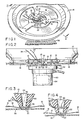
- the invention consists of a resilient pressure pad 10 secured to a rigid mounting member 12.
- the mounting member 12 is attached to a support structure 14 using screws 15.
- the support structure 14 is secured to a stationary support frame (not shown).
- a printed circuit board 16 having a polyimide film probe 18 which includes a plurality of metal test pads 20, preferably manufactured of nickel and plated on the underside of the probe 18.
- the probe 18 is covered by a ground plane except for the areas overlying the test pads 20. As a result, the probe 18 is transparent in the vicinity of the test pads 20.
- the pressure pad 10 is preferably manufactured of transparent silicone rubber or other resilient material which may be compressed and will return after compression to its original shape.
- the pad 10 includes a tip 22 preferably manufactured of a hard, transparent plastic (e.g. clear acrylic plastic).
- the pressure pad 10 and attached tip 22 are positioned directly over the polyimide film probe 18, as shown in Figs. 2 and 3.
- the pressure pad 10 includes a bore 24 through the center longitudinal axis of the pad 10 which enables a user of the testing station to look with the aid of a microscope directly downward through the pressure pad 10 and tip 22 into the transparent area of the polyimide film probe 18. This facilitates proper alignment of the polyimide film probe 18 with the integrated circuit being tested.
- the pressure pad 10 also includes a piezoelectric element 30 mounted therein.
- a piezoelectric element typically consists of a material having the ability to generate a voltage when mechanical force is applied thereto.
- the piezoelectric element 30 is preferably manufactured from barium titanate and is in the shape of a ring having an open center region 32.
- the piezoelectric element 30 is molded within the pressure pad 10 so that the bore 24 passes downwardly through the open center region 32 of the piezoelectric element 30, thereby permitting an unobstructed view through the pressure pad 10.
- the element 30 may be disc-shaped without an open center region 32 (Fig. 4).
- a suitable transparent material usable as the piezoelectric element 30 would include quartz.
- the piezoelectric element 30 further includes a plurality of electrical contact leads 34 attached thereto which permit the transmission of electrical impulses from the piezoelectric element 30 out of the pressure pad 10 to an appropriate detector or control unit, as discussed below.
- a support structure 14 is shown to which a printed circuit board 16 and polyimide film probe 18 are attached.
- the support structure 14 also includes a rigid mounting member 12 to which the pressure pad 10 is secured.
- a vacuum chuck apparatus 50 including a platform 52 and an internal stepper motor 54 for vertically moving the platform 52. Secured to the platform 52 by a vacuum generated using the vacuum chuck 50 is an integrated circuit chip or wafer 56 to be tested. To test the circuit 56, the stepper motor 54 is activated, causing elevation of the platform 52 and integrated circuit 56 upward toward the polyimide film probe 18. The integrated circuit 56 is aligned with the probe 18 by viewing downwardly through the bore 24 in the pressure pad 10. As the platform 52 of the vacuum chuck 50 moves upward with the circuit 56 thereon, the circuit 56 comes into contact with the metal test pads 20 on the underside of the polyimide film probe 18.
- the polyimide film probe 18 begins to move upward, exerting pressure on the pressure pad 10. Since the pressure pad 10 is fixedly secured to the support structure 14 using the rigid mounting member 12, significant compressive forces are generated within the pressure pad 10. The compressive forces within the pressure pad 10 cause corresponding compression of the piezoelectric element 30, thereby generating electrical impulses along and through electrical contact leads 34.
- the contact leads 34 may be connected to a suitable detector or controller which would stop the upward movement of the platform 52 and circuit 56 when a specific pressure level is reached.
- Use of the present invention permits an accurate determination of the contact pressure between the probe and circuit, permitting repeated tests of the circuit at such pressure. Repeated testing in this manner results in an improved performance evaluation of the circuit. Furthermore, a determination of pressure levels in the above manner may be used to prevent damage to the probe by the application of excessive pressure thereto.
Landscapes
- Physics & Mathematics (AREA)
- General Physics & Mathematics (AREA)
- Engineering & Computer Science (AREA)
- Computer Hardware Design (AREA)
- Microelectronics & Electronic Packaging (AREA)
- General Engineering & Computer Science (AREA)
- Testing Or Measuring Of Semiconductors Or The Like (AREA)
- Tests Of Electronic Circuits (AREA)
- Testing Of Individual Semiconductor Devices (AREA)
- Measuring Leads Or Probes (AREA)
- Measuring Fluid Pressure (AREA)
Applications Claiming Priority (2)
| Application Number | Priority Date | Filing Date | Title |
|---|---|---|---|
| US905358 | 1986-09-08 | ||
| US06/905,358 US4673839A (en) | 1986-09-08 | 1986-09-08 | Piezoelectric pressure sensing apparatus for integrated circuit testing stations |
Publications (2)
| Publication Number | Publication Date |
|---|---|
| EP0259942A2 true EP0259942A2 (de) | 1988-03-16 |
| EP0259942A3 EP0259942A3 (de) | 1989-10-04 |
Family
ID=25420688
Family Applications (1)
| Application Number | Title | Priority Date | Filing Date |
|---|---|---|---|
| EP87302425A Withdrawn EP0259942A3 (de) | 1986-09-08 | 1987-03-20 | Piezoelektrischer Druckfühler für Prüfstationen für integrierte Schaltungen |
Country Status (5)
| Country | Link |
|---|---|
| US (1) | US4673839A (de) |
| EP (1) | EP0259942A3 (de) |
| JP (1) | JPS63184349A (de) |
| KR (1) | KR880004542A (de) |
| CA (1) | CA1251288A (de) |
Cited By (2)
| Publication number | Priority date | Publication date | Assignee | Title |
|---|---|---|---|---|
| EP0460911A3 (en) * | 1990-06-08 | 1992-08-19 | Cascade Microtech, Inc. | Electrical probe with contact force protection |
| US7304488B2 (en) | 2002-05-23 | 2007-12-04 | Cascade Microtech, Inc. | Shielded probe for high-frequency testing of a device under test |
Families Citing this family (64)
| Publication number | Priority date | Publication date | Assignee | Title |
|---|---|---|---|---|
| US4701658A (en) * | 1985-03-11 | 1987-10-20 | United Technologies Corporation | Broadband acoustic point-contact transducer |
| US4811246A (en) * | 1986-03-10 | 1989-03-07 | Fitzgerald Jr William M | Micropositionable piezoelectric contactor |
| US4783719A (en) * | 1987-01-20 | 1988-11-08 | Hughes Aircraft Company | Test connector for electrical devices |
| US5189363A (en) * | 1990-09-14 | 1993-02-23 | Ibm Corporation | Integrated circuit testing system having a cantilevered contact lead probe pattern mounted on a flexible tape for interconnecting an integrated circuit to a tester |
| US5304922A (en) * | 1991-08-26 | 1994-04-19 | Hughes Aircraft Company | Electrical circuit with resilient gasket support for raised connection features |
| US5349263A (en) * | 1991-10-09 | 1994-09-20 | Mitsumi Electric Co., Ltd. | Pointing device suitable for miniaturization |
| EP0547251A1 (de) * | 1991-12-14 | 1993-06-23 | International Business Machines Corporation | Methode zum Testen eines Mikroschaltkreises |
| US6380751B2 (en) | 1992-06-11 | 2002-04-30 | Cascade Microtech, Inc. | Wafer probe station having environment control enclosure |
| US5345170A (en) | 1992-06-11 | 1994-09-06 | Cascade Microtech, Inc. | Wafer probe station having integrated guarding, Kelvin connection and shielding systems |
| US6232789B1 (en) | 1997-05-28 | 2001-05-15 | Cascade Microtech, Inc. | Probe holder for low current measurements |
| US5561377A (en) | 1995-04-14 | 1996-10-01 | Cascade Microtech, Inc. | System for evaluating probing networks |
| US5621333A (en) * | 1995-05-19 | 1997-04-15 | Microconnect, Inc. | Contact device for making connection to an electronic circuit device |
| US6046599A (en) * | 1996-05-20 | 2000-04-04 | Microconnect, Inc. | Method and device for making connection |
| US5914613A (en) | 1996-08-08 | 1999-06-22 | Cascade Microtech, Inc. | Membrane probing system with local contact scrub |
| US5949239A (en) * | 1996-09-27 | 1999-09-07 | Altera Corporation | Test head apparatus for use in electronic device test equipment |
| US5894161A (en) * | 1997-02-24 | 1999-04-13 | Micron Technology, Inc. | Interconnect with pressure sensing mechanism for testing semiconductor wafers |
| US6127831A (en) * | 1997-04-21 | 2000-10-03 | Motorola, Inc. | Method of testing a semiconductor device by automatically measuring probe tip parameters |
| US6002263A (en) | 1997-06-06 | 1999-12-14 | Cascade Microtech, Inc. | Probe station having inner and outer shielding |
| US6137299A (en) * | 1997-06-27 | 2000-10-24 | International Business Machines Corporation | Method and apparatus for testing integrated circuit chips |
| US6426636B1 (en) | 1998-02-11 | 2002-07-30 | International Business Machines Corporation | Wafer probe interface arrangement with nonresilient probe elements and support structure |
| US6256882B1 (en) | 1998-07-14 | 2001-07-10 | Cascade Microtech, Inc. | Membrane probing system |
| US6343369B1 (en) * | 1998-09-15 | 2002-01-29 | Microconnect, Inc. | Methods for making contact device for making connection to an electronic circuit device and methods of using the same |
| US6578264B1 (en) | 1999-06-04 | 2003-06-17 | Cascade Microtech, Inc. | Method for constructing a membrane probe using a depression |
| US6445202B1 (en) | 1999-06-30 | 2002-09-03 | Cascade Microtech, Inc. | Probe station thermal chuck with shielding for capacitive current |
| US6838890B2 (en) | 2000-02-25 | 2005-01-04 | Cascade Microtech, Inc. | Membrane probing system |
| US6496026B1 (en) | 2000-02-25 | 2002-12-17 | Microconnect, Inc. | Method of manufacturing and testing an electronic device using a contact device having fingers and a mechanical ground |
| US6483336B1 (en) * | 2000-05-03 | 2002-11-19 | Cascade Microtech, Inc. | Indexing rotatable chuck for a probe station |
| US6914423B2 (en) | 2000-09-05 | 2005-07-05 | Cascade Microtech, Inc. | Probe station |
| US6965226B2 (en) | 2000-09-05 | 2005-11-15 | Cascade Microtech, Inc. | Chuck for holding a device under test |
| DE10143173A1 (de) | 2000-12-04 | 2002-06-06 | Cascade Microtech Inc | Wafersonde |
| US7355420B2 (en) | 2001-08-21 | 2008-04-08 | Cascade Microtech, Inc. | Membrane probing system |
| EP1432546A4 (de) | 2001-08-31 | 2006-06-07 | Cascade Microtech Inc | Optische prüfvorrichtung |
| US6777964B2 (en) | 2002-01-25 | 2004-08-17 | Cascade Microtech, Inc. | Probe station |
| US6847219B1 (en) | 2002-11-08 | 2005-01-25 | Cascade Microtech, Inc. | Probe station with low noise characteristics |
| US6724205B1 (en) | 2002-11-13 | 2004-04-20 | Cascade Microtech, Inc. | Probe for combined signals |
| US7250779B2 (en) | 2002-11-25 | 2007-07-31 | Cascade Microtech, Inc. | Probe station with low inductance path |
| US6861856B2 (en) | 2002-12-13 | 2005-03-01 | Cascade Microtech, Inc. | Guarded tub enclosure |
| US6720789B1 (en) | 2003-02-13 | 2004-04-13 | International Business Machines Corporation | Method for wafer test and wafer test system for implementing the method |
| US7221172B2 (en) | 2003-05-06 | 2007-05-22 | Cascade Microtech, Inc. | Switched suspended conductor and connection |
| US7057404B2 (en) | 2003-05-23 | 2006-06-06 | Sharp Laboratories Of America, Inc. | Shielded probe for testing a device under test |
| US7492172B2 (en) | 2003-05-23 | 2009-02-17 | Cascade Microtech, Inc. | Chuck for holding a device under test |
| US7250626B2 (en) | 2003-10-22 | 2007-07-31 | Cascade Microtech, Inc. | Probe testing structure |
| US7187188B2 (en) | 2003-12-24 | 2007-03-06 | Cascade Microtech, Inc. | Chuck with integrated wafer support |
| WO2005065258A2 (en) | 2003-12-24 | 2005-07-21 | Cascade Microtech, Inc. | Active wafer probe |
| DE202005021434U1 (de) | 2004-06-07 | 2008-03-20 | Cascade Microtech, Inc., Beaverton | Thermooptische Einspannvorrichtung |
| US7330041B2 (en) | 2004-06-14 | 2008-02-12 | Cascade Microtech, Inc. | Localizing a temperature of a device for testing |
| KR101157449B1 (ko) | 2004-07-07 | 2012-06-22 | 캐스케이드 마이크로테크 인코포레이티드 | 멤브레인 서스펜디드 프로브를 구비한 프로브 헤드 |
| KR20070058522A (ko) | 2004-09-13 | 2007-06-08 | 캐스케이드 마이크로테크 인코포레이티드 | 양측 프루빙 구조 |
| US7656172B2 (en) | 2005-01-31 | 2010-02-02 | Cascade Microtech, Inc. | System for testing semiconductors |
| US7535247B2 (en) | 2005-01-31 | 2009-05-19 | Cascade Microtech, Inc. | Interface for testing semiconductors |
| US7167011B2 (en) * | 2005-05-27 | 2007-01-23 | Tektronix, Inc. | Differential measurement probe having retractable double cushioned variable spacing probing tips with EOS/ESD protection capabilities |
| US7253648B2 (en) * | 2005-05-27 | 2007-08-07 | Tektronix, Inc. | Signal acquisition probe having a retractable double cushioned probing tip with EOS/ESD protection capabilities |
| US7449899B2 (en) | 2005-06-08 | 2008-11-11 | Cascade Microtech, Inc. | Probe for high frequency signals |
| EP1932003A2 (de) | 2005-06-13 | 2008-06-18 | Cascade Microtech, Inc. | Breitbandige aktiv-passiv-differenzsignalsonde |
| US7609077B2 (en) | 2006-06-09 | 2009-10-27 | Cascade Microtech, Inc. | Differential signal probe with integral balun |
| US7443186B2 (en) | 2006-06-12 | 2008-10-28 | Cascade Microtech, Inc. | On-wafer test structures for differential signals |
| US7764072B2 (en) | 2006-06-12 | 2010-07-27 | Cascade Microtech, Inc. | Differential signal probing system |
| US7403028B2 (en) | 2006-06-12 | 2008-07-22 | Cascade Microtech, Inc. | Test structure and probe for differential signals |
| US7723999B2 (en) | 2006-06-12 | 2010-05-25 | Cascade Microtech, Inc. | Calibration structures for differential signal probing |
| US7876114B2 (en) | 2007-08-08 | 2011-01-25 | Cascade Microtech, Inc. | Differential waveguide probe |
| US7888957B2 (en) | 2008-10-06 | 2011-02-15 | Cascade Microtech, Inc. | Probing apparatus with impedance optimized interface |
| US8410806B2 (en) | 2008-11-21 | 2013-04-02 | Cascade Microtech, Inc. | Replaceable coupon for a probing apparatus |
| US8319503B2 (en) | 2008-11-24 | 2012-11-27 | Cascade Microtech, Inc. | Test apparatus for measuring a characteristic of a device under test |
| JP2017129395A (ja) * | 2016-01-19 | 2017-07-27 | 三菱電機株式会社 | 半導体装置の検査装置および半導体装置の検査方法 |
Family Cites Families (8)
| Publication number | Priority date | Publication date | Assignee | Title |
|---|---|---|---|---|
| US3213666A (en) * | 1962-11-29 | 1965-10-26 | Gulton Ind Inc | Impact sensor |
| US3832632A (en) * | 1971-11-22 | 1974-08-27 | F Ardezzone | Multi-point probe head assembly |
| US3810016A (en) * | 1971-12-17 | 1974-05-07 | Western Electric Co | Test probe for semiconductor devices |
| DE2344239B2 (de) * | 1973-09-01 | 1977-11-03 | Luther, Erich, 3050 Wunstorf; Maelzer, Fritz; Maelzer, Martin; 7910 Reutti Post Neu-Ulm; Türkkan, Tamer, 3011 Laatzen | Kontaktvorrichtung zum anschliessen einer gedruckten schaltung an ein pruefgeraet |
| US4079362A (en) * | 1976-07-02 | 1978-03-14 | Canadian Patents And Development Limited | Piezo-electric seed-flow monitor |
| GB2014315B (en) * | 1978-01-30 | 1983-02-02 | Texas Instruments Inc | Determining probe contact |
| US4195259A (en) * | 1978-04-04 | 1980-03-25 | Texas Instruments Incorporated | Multiprobe test system and method of using same |
| JPS58164236U (ja) * | 1982-04-27 | 1983-11-01 | 日本電気ホームエレクトロニクス株式会社 | 半導体ウエ−ハ特性測定装置 |
-
1986
- 1986-09-08 US US06/905,358 patent/US4673839A/en not_active Expired - Fee Related
-
1987
- 1987-02-24 CA CA000530444A patent/CA1251288A/en not_active Expired
- 1987-03-04 KR KR870001905A patent/KR880004542A/ko not_active Withdrawn
- 1987-03-20 EP EP87302425A patent/EP0259942A3/de not_active Withdrawn
- 1987-08-31 JP JP62217761A patent/JPS63184349A/ja active Granted
Cited By (2)
| Publication number | Priority date | Publication date | Assignee | Title |
|---|---|---|---|---|
| EP0460911A3 (en) * | 1990-06-08 | 1992-08-19 | Cascade Microtech, Inc. | Electrical probe with contact force protection |
| US7304488B2 (en) | 2002-05-23 | 2007-12-04 | Cascade Microtech, Inc. | Shielded probe for high-frequency testing of a device under test |
Also Published As
| Publication number | Publication date |
|---|---|
| EP0259942A3 (de) | 1989-10-04 |
| CA1251288A (en) | 1989-03-14 |
| JPS63184349A (ja) | 1988-07-29 |
| US4673839A (en) | 1987-06-16 |
| JPH0345541B2 (de) | 1991-07-11 |
| KR880004542A (ko) | 1988-06-04 |
Similar Documents
| Publication | Publication Date | Title |
|---|---|---|
| US4673839A (en) | Piezoelectric pressure sensing apparatus for integrated circuit testing stations | |
| US4758785A (en) | Pressure control apparatus for use in an integrated circuit testing station | |
| US6091257A (en) | Vacuum activated backside contact | |
| US6043668A (en) | Planarity verification system for integrated circuit test probes | |
| US4518914A (en) | Testing apparatus of semiconductor wafers | |
| US4665360A (en) | Docking apparatus | |
| US5461326A (en) | Self leveling and self tensioning membrane test probe | |
| US5926027A (en) | Apparatus and method for testing a device | |
| US5773986A (en) | Semiconductor wafer contact system and method for contacting a semiconductor wafer | |
| US20020057098A1 (en) | Probe contract system having planarity adjustment mechanism | |
| US5990695A (en) | Membrane test probe | |
| US9915682B2 (en) | Non-permanent termination structure for microprobe measurements | |
| US6160415A (en) | Apparatus and method for setting zero point of Z-axis in a wafer probe station | |
| JP2971491B2 (ja) | 検査装置 | |
| JPH05218149A (ja) | プローブ装置 | |
| US5898311A (en) | Shorting pad having a flexible conductive sheet | |
| JPH10209231A (ja) | プローブ装置及びプローブ装置による検査方法 | |
| US5900316A (en) | Flexible conductive sheet | |
| JPH05160210A (ja) | プローブ装置 | |
| JPH0727936B2 (ja) | プロ−ブカ−ド | |
| JPS6157699B2 (de) | ||
| JPH079439B2 (ja) | プローブ装置 | |
| JPH1079406A (ja) | 半導体ウエハ測定用プローブ装置 | |
| JPS6124244A (ja) | 半導体装置のテスタ用固定カ−ド | |
| JPH0519014A (ja) | 半導体集積回路測定治具 |
Legal Events
| Date | Code | Title | Description |
|---|---|---|---|
| PUAI | Public reference made under article 153(3) epc to a published international application that has entered the european phase |
Free format text: ORIGINAL CODE: 0009012 |
|
| AK | Designated contracting states |
Kind code of ref document: A2 Designated state(s): DE FR GB NL |
|
| PUAL | Search report despatched |
Free format text: ORIGINAL CODE: 0009013 |
|
| AK | Designated contracting states |
Kind code of ref document: A3 Designated state(s): DE FR GB NL |
|
| RHK1 | Main classification (correction) |
Ipc: G01L 1/16 |
|
| STAA | Information on the status of an ep patent application or granted ep patent |
Free format text: STATUS: THE APPLICATION IS DEEMED TO BE WITHDRAWN |
|
| 18D | Application deemed to be withdrawn |
Effective date: 19900405 |
|
| RIN1 | Information on inventor provided before grant (corrected) |
Inventor name: VEENENDAAL, CORNELIS T. |