EP0260060A1 - Selbstausrichtendes Herstellungsverfahren für bipolare Halbleiterbauelemente - Google Patents
Selbstausrichtendes Herstellungsverfahren für bipolare Halbleiterbauelemente Download PDFInfo
- Publication number
- EP0260060A1 EP0260060A1 EP87307756A EP87307756A EP0260060A1 EP 0260060 A1 EP0260060 A1 EP 0260060A1 EP 87307756 A EP87307756 A EP 87307756A EP 87307756 A EP87307756 A EP 87307756A EP 0260060 A1 EP0260060 A1 EP 0260060A1
- Authority
- EP
- European Patent Office
- Prior art keywords
- substrate
- forming
- layer
- dielectric
- dielectric layer
- Prior art date
- Legal status (The legal status is an assumption and is not a legal conclusion. Google has not performed a legal analysis and makes no representation as to the accuracy of the status listed.)
- Withdrawn
Links
Images

Classifications
-
- H—ELECTRICITY
- H10—SEMICONDUCTOR DEVICES; ELECTRIC SOLID-STATE DEVICES NOT OTHERWISE PROVIDED FOR
- H10D—INORGANIC ELECTRIC SEMICONDUCTOR DEVICES
- H10D10/00—Bipolar junction transistors [BJT]
- H10D10/01—Manufacture or treatment
- H10D10/051—Manufacture or treatment of vertical BJTs
-
- H—ELECTRICITY
- H10—SEMICONDUCTOR DEVICES; ELECTRIC SOLID-STATE DEVICES NOT OTHERWISE PROVIDED FOR
- H10D—INORGANIC ELECTRIC SEMICONDUCTOR DEVICES
- H10D10/00—Bipolar junction transistors [BJT]
- H10D10/40—Vertical BJTs
- H10D10/441—Vertical BJTs having an emitter-base junction ending at a main surface of the body and a base-collector junction ending at a lateral surface of the body
-
- H—ELECTRICITY
- H10—SEMICONDUCTOR DEVICES; ELECTRIC SOLID-STATE DEVICES NOT OTHERWISE PROVIDED FOR
- H10P—GENERIC PROCESSES OR APPARATUS FOR THE MANUFACTURE OR TREATMENT OF DEVICES COVERED BY CLASS H10
- H10P32/00—Diffusion of dopants within, into or out of wafers, substrates or parts of devices
- H10P32/10—Diffusion of dopants within, into or out of semiconductor bodies or layers
- H10P32/14—Diffusion of dopants within, into or out of semiconductor bodies or layers within a single semiconductor body or layer in a solid phase; between different semiconductor bodies or layers, both in a solid phase
- H10P32/1408—Diffusion of dopants within, into or out of semiconductor bodies or layers within a single semiconductor body or layer in a solid phase; between different semiconductor bodies or layers, both in a solid phase from or through or into an external applied layer, e.g. photoresist or nitride layers
- H10P32/1414—Diffusion of dopants within, into or out of semiconductor bodies or layers within a single semiconductor body or layer in a solid phase; between different semiconductor bodies or layers, both in a solid phase from or through or into an external applied layer, e.g. photoresist or nitride layers the applied layer being silicon, silicide or SIPOS, e.g. polysilicon or porous silicon
-
- H—ELECTRICITY
- H10—SEMICONDUCTOR DEVICES; ELECTRIC SOLID-STATE DEVICES NOT OTHERWISE PROVIDED FOR
- H10P—GENERIC PROCESSES OR APPARATUS FOR THE MANUFACTURE OR TREATMENT OF DEVICES COVERED BY CLASS H10
- H10P32/00—Diffusion of dopants within, into or out of wafers, substrates or parts of devices
- H10P32/10—Diffusion of dopants within, into or out of semiconductor bodies or layers
- H10P32/17—Diffusion of dopants within, into or out of semiconductor bodies or layers characterised by the semiconductor material
- H10P32/171—Diffusion of dopants within, into or out of semiconductor bodies or layers characterised by the semiconductor material being group IV material
-
- H—ELECTRICITY
- H10—SEMICONDUCTOR DEVICES; ELECTRIC SOLID-STATE DEVICES NOT OTHERWISE PROVIDED FOR
- H10P—GENERIC PROCESSES OR APPARATUS FOR THE MANUFACTURE OR TREATMENT OF DEVICES COVERED BY CLASS H10
- H10P76/00—Manufacture or treatment of masks on semiconductor bodies, e.g. by lithography or photolithography
- H10P76/40—Manufacture or treatment of masks on semiconductor bodies, e.g. by lithography or photolithography of masks comprising inorganic materials
-
- H—ELECTRICITY
- H10—SEMICONDUCTOR DEVICES; ELECTRIC SOLID-STATE DEVICES NOT OTHERWISE PROVIDED FOR
- H10W—GENERIC PACKAGES, INTERCONNECTIONS, CONNECTORS OR OTHER CONSTRUCTIONAL DETAILS OF DEVICES COVERED BY CLASS H10
- H10W10/00—Isolation regions in semiconductor bodies between components of integrated devices
- H10W10/01—Manufacture or treatment
- H10W10/011—Manufacture or treatment of isolation regions comprising dielectric materials
- H10W10/012—Manufacture or treatment of isolation regions comprising dielectric materials using local oxidation of silicon [LOCOS]
- H10W10/0121—Manufacture or treatment of isolation regions comprising dielectric materials using local oxidation of silicon [LOCOS] in regions recessed from the surface, e.g. in trenches or grooves
-
- H—ELECTRICITY
- H10—SEMICONDUCTOR DEVICES; ELECTRIC SOLID-STATE DEVICES NOT OTHERWISE PROVIDED FOR
- H10W—GENERIC PACKAGES, INTERCONNECTIONS, CONNECTORS OR OTHER CONSTRUCTIONAL DETAILS OF DEVICES COVERED BY CLASS H10
- H10W10/00—Isolation regions in semiconductor bodies between components of integrated devices
- H10W10/01—Manufacture or treatment
- H10W10/011—Manufacture or treatment of isolation regions comprising dielectric materials
- H10W10/012—Manufacture or treatment of isolation regions comprising dielectric materials using local oxidation of silicon [LOCOS]
- H10W10/0125—Manufacture or treatment of isolation regions comprising dielectric materials using local oxidation of silicon [LOCOS] comprising introducing electrical impurities in local oxidation regions, e.g. to alter LOCOS oxide growth characteristics
- H10W10/0126—Manufacture or treatment of isolation regions comprising dielectric materials using local oxidation of silicon [LOCOS] comprising introducing electrical impurities in local oxidation regions, e.g. to alter LOCOS oxide growth characteristics introducing electrical active impurities in local oxidation regions to create channel stoppers
-
- H—ELECTRICITY
- H10—SEMICONDUCTOR DEVICES; ELECTRIC SOLID-STATE DEVICES NOT OTHERWISE PROVIDED FOR
- H10W—GENERIC PACKAGES, INTERCONNECTIONS, CONNECTORS OR OTHER CONSTRUCTIONAL DETAILS OF DEVICES COVERED BY CLASS H10
- H10W10/00—Isolation regions in semiconductor bodies between components of integrated devices
- H10W10/10—Isolation regions comprising dielectric materials
- H10W10/13—Isolation regions comprising dielectric materials formed using local oxidation of silicon [LOCOS], e.g. sealed interface localised oxidation [SILO] or side-wall mask isolation [SWAMI]
-
- Y—GENERAL TAGGING OF NEW TECHNOLOGICAL DEVELOPMENTS; GENERAL TAGGING OF CROSS-SECTIONAL TECHNOLOGIES SPANNING OVER SEVERAL SECTIONS OF THE IPC; TECHNICAL SUBJECTS COVERED BY FORMER USPC CROSS-REFERENCE ART COLLECTIONS [XRACs] AND DIGESTS
- Y10—TECHNICAL SUBJECTS COVERED BY FORMER USPC
- Y10S—TECHNICAL SUBJECTS COVERED BY FORMER USPC CROSS-REFERENCE ART COLLECTIONS [XRACs] AND DIGESTS
- Y10S148/00—Metal treatment
- Y10S148/01—Bipolar transistors-ion implantation
-
- Y—GENERAL TAGGING OF NEW TECHNOLOGICAL DEVELOPMENTS; GENERAL TAGGING OF CROSS-SECTIONAL TECHNOLOGIES SPANNING OVER SEVERAL SECTIONS OF THE IPC; TECHNICAL SUBJECTS COVERED BY FORMER USPC CROSS-REFERENCE ART COLLECTIONS [XRACs] AND DIGESTS
- Y10—TECHNICAL SUBJECTS COVERED BY FORMER USPC
- Y10S—TECHNICAL SUBJECTS COVERED BY FORMER USPC CROSS-REFERENCE ART COLLECTIONS [XRACs] AND DIGESTS
- Y10S148/00—Metal treatment
- Y10S148/011—Bipolar transistors
-
- Y—GENERAL TAGGING OF NEW TECHNOLOGICAL DEVELOPMENTS; GENERAL TAGGING OF CROSS-SECTIONAL TECHNOLOGIES SPANNING OVER SEVERAL SECTIONS OF THE IPC; TECHNICAL SUBJECTS COVERED BY FORMER USPC CROSS-REFERENCE ART COLLECTIONS [XRACs] AND DIGESTS
- Y10—TECHNICAL SUBJECTS COVERED BY FORMER USPC
- Y10S—TECHNICAL SUBJECTS COVERED BY FORMER USPC CROSS-REFERENCE ART COLLECTIONS [XRACs] AND DIGESTS
- Y10S148/00—Metal treatment
- Y10S148/124—Polycrystalline emitter
Definitions
- This invention relates to bipolar semiconductor devices and to processes for their fabrication.
- Bipolar devices fabricated using known processes are limited in terms of performance by base resistance and capacitance. If the performance of bipolar devices is to be improved, it will be necessary to reduce the area of the base. Considerable attention has already been given to the reduction of base area and the scope for further reduction is severely limited by alignment tolerances for the base and emitter contacts and the limits of resolution of the lithographic process. Consequently there exists a need for an improved fabrication process which will enable the fabrication of bipolar devices having bases of reduced area without the need to define small device dimensions lithographically.
- the present invention seeks to provide an improved fabrication method by means of which the base contact area can be reduced with consequent improvements in device performance.
- the term 'substrate' unless the context clearly required otherwise, is used to refer to the semiconductor in which the active areas of the transistor are grown and includes any epitaxial semiconductor layers in which active areas are formed.
- a method of fabricating a bipolar transistor comprising emitter, base and collector regions in a semiconductor substrate, the method comprising the steps of:
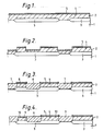
- Figure 1 to 8 are diagrammatic cross-sections through a device according to the invention at various stages of its production.
- the starting point for the process according to the invention is a p-type silicon substrate as conventionally prepared for bipolar circuits with buried layers.
- Figure 1 shows such a precursor with a p-type substrate (1), 1-1.5 um thick n-type epitaxial layer (2) and an n+ buried layer (3) at the interface therebetween.
- a thin oxide layer (4) 10-30 nm thick, is formed on the epitaxial layer.
- a nitride layer (5) approximately 200 nm thick is formed over the oxide layer (4).
- the nitride layer (5) is then cut to expose the silicon of the epitaxial layer apart from in those areas which will subsequently form the collector sinker and the active area.
- the exposed silicon is then removed by plasma etching to a depth of about 0.5 to 0.7 um.
- the structure at this stage is as shown in Figure 2.
- Boron is implanted into the exposed silicon to form a channel stopper.
- the exposed silicon is then oxidised using, for example, the LOCOS process to give oxide islands (6 and 7) taking the place of the etched silicon.
- Oxide is grown until its upper surface is approximately at the level of the upper surface of the epitaxial silicon layer.
- boron diffuses towards the substrate, thereby providing device isolation.
- the device structure is as shown in Figure 3.
- the nitride and thin oxide is then stripped from the area (8) which is to become the collector sinker.
- the collector contact is implanted with antimony or arsenic to produce a region of n+ semiconductor.
- a thin oxide coating (10) is grown over the collector contact (9). The structure at this point is as shown in Figure 4.
- a 0.5-1.0 um thick nitride layer (11) is next deposited.
- This thick nitride layer is patterned and cut to leave a substitute emitter (12) on the thin nitride layer (5) which covers the active area (13) of the device.
- the active area adjacent the substitute emitter (12) is then implanted with, for example, boron to produce p+ regions (14) near the surface of the silicon of the active area.
- the thin oxide layer (4) over the active area is stripped either before or after the boron implant, but before deposition of the polysilicon layer which is to be deposited next.
- Polysilicon is deposited conformally to a depth of about 0.5 to 1 um.
- a thin layer of a metal (Ti, Co, W, Pt, Mo, Ta) is deposited over the polysilicon and reacted to form a silicide.
- the resulting polycide (24) is then planarised to produce a structure as shown in Figure 5.
- the polycide (24) is patterned and etched away everywhere except over the active area and over part of the adjoining oxide islands (6 and 7) to leave polycide/polysilicon base contacts which are then oxidised to a depth of about 200 nm. During the oxidation step the thickness of the oxide on the collector contact is of course increased.
- the structure at this stage is as shown in Figure 6.
- the substitute emitter is removed by etching.
- the base region (15) is then implanted through the opening left by removal of the substitute emitter with p-type impurities either through the thin oxide layer (4) or after its removal.
- a layer (16) of oxide is then formed and cut to produce sidewall spacers (17 and 18) on either side of the polysilicon contacts.
- the structure at this stage is as shown in Figure 7.
- n+ polysilicon emitter contact is formed by depositing, doping (during or after deposition) and cutting a polysilicon layer. A short anneal is performed and the n-type dopant diffuses from the polysilicon into the single crystal silicon to form a shallow emitter. Further processing, including deposition of another dielectric layer, the cutting of contacts and metallisation is conventional.
Landscapes
- Bipolar Transistors (AREA)
Applications Claiming Priority (2)
| Application Number | Priority Date | Filing Date | Title |
|---|---|---|---|
| GB8621534 | 1986-09-08 | ||
| GB868621534A GB8621534D0 (en) | 1986-09-08 | 1986-09-08 | Bipolar fabrication process |
Publications (1)
| Publication Number | Publication Date |
|---|---|
| EP0260060A1 true EP0260060A1 (de) | 1988-03-16 |
Family
ID=10603811
Family Applications (1)
| Application Number | Title | Priority Date | Filing Date |
|---|---|---|---|
| EP87307756A Withdrawn EP0260060A1 (de) | 1986-09-08 | 1987-09-02 | Selbstausrichtendes Herstellungsverfahren für bipolare Halbleiterbauelemente |
Country Status (3)
| Country | Link |
|---|---|
| US (1) | US4801556A (de) |
| EP (1) | EP0260060A1 (de) |
| GB (1) | GB8621534D0 (de) |
Cited By (2)
| Publication number | Priority date | Publication date | Assignee | Title |
|---|---|---|---|---|
| EP0346535A1 (de) * | 1987-02-27 | 1989-12-20 | BRITISH TELECOMMUNICATIONS public limited company | Selbstausrichtendes bipolares Herstellungsverfahren |
| EP0443253A1 (de) * | 1990-02-20 | 1991-08-28 | AT&T Corp. | Selbstjustierte Kontakt-Technologie |
Families Citing this family (5)
| Publication number | Priority date | Publication date | Assignee | Title |
|---|---|---|---|---|
| US4927774A (en) * | 1988-06-10 | 1990-05-22 | British Telecommunications Plc | Self aligned bipolar fabrication process |
| JPH0226032A (ja) * | 1988-07-14 | 1990-01-29 | Matsushita Electric Ind Co Ltd | 半導体装置の製造方法 |
| US5236851A (en) * | 1988-07-14 | 1993-08-17 | Matsushita Electric Industrial Co., Ltd. | Method for fabricating semiconductor devices |
| US5001538A (en) * | 1988-12-28 | 1991-03-19 | Synergy Semiconductor Corporation | Bipolar sinker structure and process for forming same |
| US6703679B1 (en) | 1999-08-31 | 2004-03-09 | Analog Devices, Imi, Inc. | Low-resistivity microelectromechanical structures with co-fabricated integrated circuit |
Citations (2)
| Publication number | Priority date | Publication date | Assignee | Title |
|---|---|---|---|---|
| EP0036499B1 (de) * | 1980-03-24 | 1984-08-15 | International Business Machines Corporation | Ein selbstjustierendes Verfahren für einen Bipolartransistor auf Polysilicium-Basis |
| US4492008A (en) * | 1983-08-04 | 1985-01-08 | International Business Machines Corporation | Methods for making high performance lateral bipolar transistors |
Family Cites Families (1)
| Publication number | Priority date | Publication date | Assignee | Title |
|---|---|---|---|---|
| US4338138A (en) * | 1980-03-03 | 1982-07-06 | International Business Machines Corporation | Process for fabricating a bipolar transistor |
-
1986
- 1986-09-08 GB GB868621534A patent/GB8621534D0/en active Pending
-
1987
- 1987-09-02 EP EP87307756A patent/EP0260060A1/de not_active Withdrawn
- 1987-09-08 US US07/093,667 patent/US4801556A/en not_active Expired - Fee Related
Patent Citations (2)
| Publication number | Priority date | Publication date | Assignee | Title |
|---|---|---|---|---|
| EP0036499B1 (de) * | 1980-03-24 | 1984-08-15 | International Business Machines Corporation | Ein selbstjustierendes Verfahren für einen Bipolartransistor auf Polysilicium-Basis |
| US4492008A (en) * | 1983-08-04 | 1985-01-08 | International Business Machines Corporation | Methods for making high performance lateral bipolar transistors |
Non-Patent Citations (1)
| Title |
|---|
| IBM TECHNICAL DISCLOSURE BULLETIN, vol. 24, no. 3, August 1981, pages 1745,1746, New York, US; I. ANTIPOV: "Method for making lateral PNP devices" * |
Cited By (2)
| Publication number | Priority date | Publication date | Assignee | Title |
|---|---|---|---|---|
| EP0346535A1 (de) * | 1987-02-27 | 1989-12-20 | BRITISH TELECOMMUNICATIONS public limited company | Selbstausrichtendes bipolares Herstellungsverfahren |
| EP0443253A1 (de) * | 1990-02-20 | 1991-08-28 | AT&T Corp. | Selbstjustierte Kontakt-Technologie |
Also Published As
| Publication number | Publication date |
|---|---|
| US4801556A (en) | 1989-01-31 |
| GB8621534D0 (en) | 1986-10-15 |
Similar Documents
| Publication | Publication Date | Title |
|---|---|---|
| EP0036082B1 (de) | Selbstjustierendes Verfahren zur Herstellung eines verbesserten hochqualitativen Bipolartransistors | |
| US5614750A (en) | Buried layer contact for an integrated circuit structure | |
| KR950003932B1 (ko) | 바이폴라형 반도체장치의 제조방법 | |
| US4994400A (en) | Method of fabricating a semiconductor device using a tri-layer structure and conductive sidewalls | |
| US5434092A (en) | Method for fabricating a triple self-aligned bipolar junction transistor | |
| US5323057A (en) | Lateral bipolar transistor with insulating trenches | |
| JPH0628266B2 (ja) | 半導体装置の製造方法 | |
| US4997775A (en) | Method for forming a complementary bipolar transistor structure including a self-aligned vertical PNP transistor | |
| US4871684A (en) | Self-aligned polysilicon emitter and contact structure for high performance bipolar transistors | |
| EP1273036B1 (de) | Verfahren zur herstellung einer heteroübergang-bicmos-integrierter schaltung | |
| JPH0630359B2 (ja) | バイポーラトランジスタの製造方法 | |
| EP0258147A2 (de) | Verfahren zum Herstellen eines bipolaren Transistors mit einem Streifen aus Polysilizium | |
| US6767797B2 (en) | Method of fabricating complementary self-aligned bipolar transistors | |
| JP2587444B2 (ja) | Cmos技術を用いたバイポーラ・トランジスタとその製造方法 | |
| JPH04330730A (ja) | 半導体装置及びその製造方法 | |
| US4801556A (en) | Self-aligned bipolar fabrication process | |
| US6706583B1 (en) | High speed low noise transistor | |
| US5149663A (en) | Method for manufacturing a Bi-CMOS semiconductor device | |
| JPS62194673A (ja) | 半導体装置の製造方法 | |
| US6444536B2 (en) | Method for fabricating bipolar transistors | |
| EP0231740A2 (de) | Selbstjustierendes bipolares Bauelement aus Polysilizium und Verfahren zu seiner Herstellung | |
| US6197649B1 (en) | Process for manufacturing planar fast recovery diode using reduced number of masking steps | |
| US6060365A (en) | Method for fabricating a bipolar transistor | |
| EP1298718A2 (de) | Verfahren zur Herstellung und Struktur einer Halbleitervorrichtung mit einer Sinker-Kontaktregion | |
| EP0260058A1 (de) | Selbstausrichtendes Herstellungsverfahren für bipolare Halbleiterbauelemente |
Legal Events
| Date | Code | Title | Description |
|---|---|---|---|
| PUAI | Public reference made under article 153(3) epc to a published international application that has entered the european phase |
Free format text: ORIGINAL CODE: 0009012 |
|
| AK | Designated contracting states |
Kind code of ref document: A1 Designated state(s): AT BE CH DE ES FR GB GR IT LI LU NL SE |
|
| 17P | Request for examination filed |
Effective date: 19880819 |
|
| RAP3 | Party data changed (applicant data changed or rights of an application transferred) |
Owner name: BRITISH TELECOMMUNICATIONS PUBLIC LIMITED COMPANY |
|
| 17Q | First examination report despatched |
Effective date: 19900702 |
|
| STAA | Information on the status of an ep patent application or granted ep patent |
Free format text: STATUS: THE APPLICATION IS DEEMED TO BE WITHDRAWN |
|
| 18D | Application deemed to be withdrawn |
Effective date: 19901113 |
|
| RIN1 | Information on inventor provided before grant (corrected) |
Inventor name: WELBOURN, ANTHONY DAVID Inventor name: HESLOP, CHRISTOPHER JOHN HEDLEY |