EP0261905A2 - Elektrischer Verbinder und Verfahren zur Verbindung von Adern an diesem - Google Patents
Elektrischer Verbinder und Verfahren zur Verbindung von Adern an diesem Download PDFInfo
- Publication number
- EP0261905A2 EP0261905A2 EP87308321A EP87308321A EP0261905A2 EP 0261905 A2 EP0261905 A2 EP 0261905A2 EP 87308321 A EP87308321 A EP 87308321A EP 87308321 A EP87308321 A EP 87308321A EP 0261905 A2 EP0261905 A2 EP 0261905A2
- Authority
- EP
- European Patent Office
- Prior art keywords
- conductors
- crimp
- solder
- bus bar
- connector
- Prior art date
- Legal status (The legal status is an assumption and is not a legal conclusion. Google has not performed a legal analysis and makes no representation as to the accuracy of the status listed.)
- Granted
Links
- 238000000034 method Methods 0.000 title claims abstract description 33
- 239000004020 conductor Substances 0.000 claims abstract description 38
- 229910000679 solder Inorganic materials 0.000 claims abstract description 31
- 238000002788 crimping Methods 0.000 claims abstract description 17
- 238000010438 heat treatment Methods 0.000 claims abstract description 7
- 238000007747 plating Methods 0.000 claims description 13
- 230000001154 acute effect Effects 0.000 claims description 2
- 238000005452 bending Methods 0.000 claims 1
- 230000005540 biological transmission Effects 0.000 abstract description 2
- 230000005405 multipole Effects 0.000 description 7
- 239000012212 insulator Substances 0.000 description 5
- 238000005476 soldering Methods 0.000 description 5
- 238000010923 batch production Methods 0.000 description 4
- 239000002184 metal Substances 0.000 description 3
- 229910052751 metal Inorganic materials 0.000 description 3
- 239000004809 Teflon Substances 0.000 description 2
- 229920006362 Teflon® Polymers 0.000 description 2
- ATJFFYVFTNAWJD-UHFFFAOYSA-N Tin Chemical compound [Sn] ATJFFYVFTNAWJD-UHFFFAOYSA-N 0.000 description 2
- 238000003825 pressing Methods 0.000 description 2
- 230000035939 shock Effects 0.000 description 2
- BFKJFAAPBSQJPD-UHFFFAOYSA-N tetrafluoroethene Chemical compound FC(F)=C(F)F BFKJFAAPBSQJPD-UHFFFAOYSA-N 0.000 description 2
- RYGMFSIKBFXOCR-UHFFFAOYSA-N Copper Chemical compound [Cu] RYGMFSIKBFXOCR-UHFFFAOYSA-N 0.000 description 1
- 229910052802 copper Inorganic materials 0.000 description 1
- 239000010949 copper Substances 0.000 description 1
- 230000007547 defect Effects 0.000 description 1
- 238000010586 diagram Methods 0.000 description 1
- 238000006073 displacement reaction Methods 0.000 description 1
- 230000001771 impaired effect Effects 0.000 description 1
- 230000006698 induction Effects 0.000 description 1
- 239000011810 insulating material Substances 0.000 description 1
- 239000000463 material Substances 0.000 description 1
- 238000002844 melting Methods 0.000 description 1
- 230000008018 melting Effects 0.000 description 1
- 150000002739 metals Chemical class 0.000 description 1
- 238000012986 modification Methods 0.000 description 1
- 230000004048 modification Effects 0.000 description 1
- 230000003647 oxidation Effects 0.000 description 1
- 238000007254 oxidation reaction Methods 0.000 description 1
- 238000004080 punching Methods 0.000 description 1
- 238000000926 separation method Methods 0.000 description 1
- 230000008054 signal transmission Effects 0.000 description 1
- 238000003466 welding Methods 0.000 description 1
Images



Classifications
-
- H—ELECTRICITY
- H01—ELECTRIC ELEMENTS
- H01R—ELECTRICALLY-CONDUCTIVE CONNECTIONS; STRUCTURAL ASSOCIATIONS OF A PLURALITY OF MUTUALLY-INSULATED ELECTRICAL CONNECTING ELEMENTS; COUPLING DEVICES; CURRENT COLLECTORS
- H01R12/00—Structural associations of a plurality of mutually-insulated electrical connecting elements, specially adapted for printed circuits, e.g. printed circuit boards [PCB], flat or ribbon cables, or like generally planar structures, e.g. terminal strips, terminal blocks; Coupling devices specially adapted for printed circuits, flat or ribbon cables, or like generally planar structures; Terminals specially adapted for contact with, or insertion into, printed circuits, flat or ribbon cables, or like generally planar structures
- H01R12/50—Fixed connections
- H01R12/59—Fixed connections for flexible printed circuits, flat or ribbon cables or like structures
- H01R12/592—Fixed connections for flexible printed circuits, flat or ribbon cables or like structures connections to contact elements
-
- H—ELECTRICITY
- H01—ELECTRIC ELEMENTS
- H01R—ELECTRICALLY-CONDUCTIVE CONNECTIONS; STRUCTURAL ASSOCIATIONS OF A PLURALITY OF MUTUALLY-INSULATED ELECTRICAL CONNECTING ELEMENTS; COUPLING DEVICES; CURRENT COLLECTORS
- H01R4/00—Electrically-conductive connections between two or more conductive members in direct contact, i.e. touching one another; Means for effecting or maintaining such contact; Electrically-conductive connections having two or more spaced connecting locations for conductors and using contact members penetrating insulation
- H01R4/10—Electrically-conductive connections between two or more conductive members in direct contact, i.e. touching one another; Means for effecting or maintaining such contact; Electrically-conductive connections having two or more spaced connecting locations for conductors and using contact members penetrating insulation effected solely by twisting, wrapping, bending, crimping, or other permanent deformation
- H01R4/18—Electrically-conductive connections between two or more conductive members in direct contact, i.e. touching one another; Means for effecting or maintaining such contact; Electrically-conductive connections having two or more spaced connecting locations for conductors and using contact members penetrating insulation effected solely by twisting, wrapping, bending, crimping, or other permanent deformation by crimping
-
- H—ELECTRICITY
- H01—ELECTRIC ELEMENTS
- H01R—ELECTRICALLY-CONDUCTIVE CONNECTIONS; STRUCTURAL ASSOCIATIONS OF A PLURALITY OF MUTUALLY-INSULATED ELECTRICAL CONNECTING ELEMENTS; COUPLING DEVICES; CURRENT COLLECTORS
- H01R4/00—Electrically-conductive connections between two or more conductive members in direct contact, i.e. touching one another; Means for effecting or maintaining such contact; Electrically-conductive connections having two or more spaced connecting locations for conductors and using contact members penetrating insulation
- H01R4/02—Soldered or welded connections
-
- H—ELECTRICITY
- H01—ELECTRIC ELEMENTS
- H01R—ELECTRICALLY-CONDUCTIVE CONNECTIONS; STRUCTURAL ASSOCIATIONS OF A PLURALITY OF MUTUALLY-INSULATED ELECTRICAL CONNECTING ELEMENTS; COUPLING DEVICES; CURRENT COLLECTORS
- H01R43/00—Apparatus or processes specially adapted for manufacturing, assembling, maintaining, or repairing of line connectors or current collectors or for joining electric conductors
- H01R43/04—Apparatus or processes specially adapted for manufacturing, assembling, maintaining, or repairing of line connectors or current collectors or for joining electric conductors for forming connections by deformation, e.g. crimping tool
- H01R43/048—Crimping apparatus or processes
-
- Y—GENERAL TAGGING OF NEW TECHNOLOGICAL DEVELOPMENTS; GENERAL TAGGING OF CROSS-SECTIONAL TECHNOLOGIES SPANNING OVER SEVERAL SECTIONS OF THE IPC; TECHNICAL SUBJECTS COVERED BY FORMER USPC CROSS-REFERENCE ART COLLECTIONS [XRACs] AND DIGESTS
- Y10—TECHNICAL SUBJECTS COVERED BY FORMER USPC
- Y10T—TECHNICAL SUBJECTS COVERED BY FORMER US CLASSIFICATION
- Y10T29/00—Metal working
- Y10T29/49—Method of mechanical manufacture
- Y10T29/49002—Electrical device making
- Y10T29/49117—Conductor or circuit manufacturing
- Y10T29/49174—Assembling terminal to elongated conductor
- Y10T29/49179—Assembling terminal to elongated conductor by metal fusion bonding
-
- Y—GENERAL TAGGING OF NEW TECHNOLOGICAL DEVELOPMENTS; GENERAL TAGGING OF CROSS-SECTIONAL TECHNOLOGIES SPANNING OVER SEVERAL SECTIONS OF THE IPC; TECHNICAL SUBJECTS COVERED BY FORMER USPC CROSS-REFERENCE ART COLLECTIONS [XRACs] AND DIGESTS
- Y10—TECHNICAL SUBJECTS COVERED BY FORMER USPC
- Y10T—TECHNICAL SUBJECTS COVERED BY FORMER US CLASSIFICATION
- Y10T29/00—Metal working
- Y10T29/49—Method of mechanical manufacture
- Y10T29/49002—Electrical device making
- Y10T29/49117—Conductor or circuit manufacturing
- Y10T29/49204—Contact or terminal manufacturing
- Y10T29/49208—Contact or terminal manufacturing by assembling plural parts
- Y10T29/49218—Contact or terminal manufacturing by assembling plural parts with deforming
Definitions
- the field of the invention relates to a method for connecting wires, particularly those within high density, flat transmission cables, to multipole connectors, and a crimp type micro-multipole connector for facilitating said method.
- IDC connections in many applications are made through such commonly known methods such as soldering, spot welding and lapping.
- crimp type connections and insulator displacement connections are more popular for connecting conductors to electrical connectors.
- the former method includes the clamping of a crimp barrel formed on the tail portion of a contact member about a conductor.
- the latter involves the pressing of an insulated wire into an IDC contact member having a U-shaped slot.
- Crimp connections are mainly used for connecting a single wire to a single crimp type contact member.
- IDC connections are generally employed in mass type connecting procedures wherin a plurality of conductors in a flat cable or ribbon cable are connected to IDC connectors having appropriately designed contacts therein.
- a high density signal transmission cable may have a plurality of signal conductors (e.g. 24), each having a diameter of about 0.20mm distributed along 1.27mm center lines. Grounding wires of about 0.254mm diameter are provided on both sides of the signal wires and spaced about 0.46mm therefrom. There is accordingly a space of about 0.35mm between adjacent grounding wires.
- various types of 1.27mm pitch multipole micro-connectors are employed.
- a plurality of wires in the flat cable may, for example, be simultaneously pressed into IDC contact members in an IDC type connector.
- a crimp barrel of a contact member is crimped to a conductor of an insulated wire and, thereafter, a plurality of contact members so crimped are successively inserted into the cavities of an insulator or housing.
- the method using IDC connectors has been preferred because of its simplicity.
- Such processes would include utilizing a preassembly housing having a plurality of contact members therein, each contact member having a crimp section.
- the conductors of the flat cable would be inserted within the crimp sections and the crimp sections compressed simultaneously. It would be very difficult to assure reliable electrical connection at this high rate, however.
- the spacing of the comb-shaped teeth of a punch or crimper used for such a micro-connector would be so small that the strength of the crimper would be substantially reduced.
- Delicate controls would be required for installing the crimper and corresponding anvil and maintaining them during the crimping process.
- soldering is also unacceptable as it would cause a short circuit between adjacent conductors due to fluctuation of the solder supply.
- the method provided by the invention emloys both crimp connection technology and a soldering technique.
- a contact member is provided having a crimping section.
- the crimping section is plated with solder. Once a conductor has been inserted within the crimping section, the crimping section is pressed into contact with the conductor. Heat is then applied to the crimping section to fuse the solder. Reliable solder connections between the crimping section and conductor are made as the solder adheres to these mutually contacting members. Once the solder is cooled, the connection will be very resistant to shocks and vibration.
- a bus bar is employed together with contacts having crimping sections. Both the bus bar and crimping sections are solder-plated.
- the grounding wires are secured to the bus bar which, in turn, is secured to the cable.
- the signal wires are crimped to the contacts, the contacts being mounted to an insulator. Thereafter, in order to solder the bus bar to the grounding wires, and the crimping sections to the signal wires in a batch process, the entire solder-plated assembly is heated to fuse the solder.
- a crimp type, micro-multipole connector is also provided by the invention which facilitates the practice of the method according to the invention.
- the flat cable 12 includes a plurality of parallel signal wires 14 and ground wires 16, all of which may be silver-plated copper wires.
- the wires are supported by a flexible insulator film made from TEFLON or the like.
- Twenty-four signal wires 18 and forty-eight grounding wires 20 are provided within the high density cable 12.
- the signal wires each have a diameter of about 0.20mm while the grounding wires have about 0.254mm diameter.
- a spacing of about 0.46mm is provided between signal and ground wires.
- the spacing between signal wires is about 1.27mm.
- the spacing between adjacent grounding wires is accordingly about 0.35mm.
- the multipole connector 10 includes an insulator housing 22 which defines upper and lower rows of thirteen cavities 24.
- Female contacts 26 are positioned within each cavity. Projections 28 extending laterally from the contacts maintain them within the respective cavities.
- Each contact includes a crimp barrel 30 projecting from the rear side of the housing 22. The spacing between crimp barrels is the same as that between signal wires, i.e. about 1.27mm.
- Each crimp barrel 30 includes a solder plating 32 as shown in Fig. 9B.
- the plating is preferably twenty to thirty microns in thickness, which is exceptionally large compared with the tin plating of several microns often used on contacts, and is applied prior to mounting the contacts to the housing.
- a solder composition of seventy-five percent tin and twenty-five percent lead is suitable for the purposes of the invention, although other percentages of these metals could also be successfully employed.
- Each contact 26 includes a pair of opposing spring members 34 positioned within one of the cavities for receiving a pin 36 of a male connector.
- a representative arrangement of contacts is shown in Fig. 3. The encircled numerals indicate the post numbers of the contacts to be grounded.
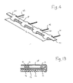
- a bus bar 38 for soldering the grounding wires 16 of the flat cable 12 and connecting them to ground is shown in Fig. 4.
- the bus bar is generally c-shaped, and may be formed by pressing and punching. It is also entirely plated with a thick solder plating between twenty and thirty microns.
- a plurality of slots 40 are formed in one end of the bus bar while integral ground pins 42 extend from the other end thereof. A total of six ground pins are provided to correspond with the contact members to be grounded as shown in Fig. 3.
- the slots 40 are of appropriate size to receive the grounding wires 16 of the cable.
- a pair of laterally extending tabs 44 are provided for securing the bus bar the cable.
- the bus bar which has substantially the same width as that of the cable, is initially secured to the cable by inserting the ends of selected cable wires into the slots 40.
- the wire ends are exposed by peeling off the cable film near one end of the cable as shown in Fig. 2.
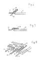
- the exposed ends of the grounding wires 16 and of six signal wires 14 corresponding to the positions of the grounding pins 42 are bent back to form an acute angle with the cable surface.
- Fig. 5 is illustrative of a cable end portion having grounding wires bent back in this position.
- the bent wires are inserted into the slots 40 of the bus bar as shown in Fig. 6.
- the bus bar is then moved into contact with the cable surface (Fig. 7), the lateral tabs 44 thereof being bent to secure the bus bar to the cable.
- the method according to the invention includes applying a thick solder plating to the crimp barrels prior to mounting the contacts 26 within the connector.
- the crimping process (Figs. 10A, 10B) is performed upon all barrels simultaneously in a well-known process.
- the crimper (not shown) employed in this procedure includes twenty-six punches arranged at a pitch of 1.27mm and an anvil. The plated interior surfaces of the crimp barrels 30 and the wires 14 and pins 42 therein are brought into physical contact with each other as shown in Fig. 10B through the crimping process.
- the crimping of the crimp barrels in accordance with the invention is not necessarily intended to achieve the high reliability of electrical connections for which crimping is conventionally employed. It is sufficient if the crimp barrels and conductors are in sufficiently close proximity, and preferably in contact with each other, so that melting solder will tend to move between the respective crimp barrels and conductors under the forces of capillary action as explained hereinafter.
- Figs. 11-13 illustrate the final step through which highly reliable electrical connections are made in a batch process.
- the bus bar 38, crimp barrels 30, and conductors 14,42 within the crimp barrels are exposed to a heat source such as a high frequency induction heating device 50. This fuses the solder plating applied to the crimp barrels and bus bar.
- the grounding wires 16 and bus bar 38, and signal wires 14 and crimp barrels, are respectively soldered together as the assembly is allowed to cool.
- the bus bar is preferably pressed during the heating operation.
- the fused solder expands over the metal surfaces to be connected due to capillarity. In order to insure proper flow of the solder, it must be heated to an appropriate temperature . and all metal surfaces must be clean. It is also advantageous if the insulating material for the flat cable be heat resistant. The use of TEFLON material for this purpose has been found to be satisfactory.
- the bus bar and conductors of the flat cable can be heated to complete soldering prior to placing the signal wires within the crimp barrels and employing the crimper therewith.
- the bus bar may be entirely omitted.
- the invention allows the connection of a flat cable or the like having small, closely spaced conductors to be reliably connected to an electrical connector in a batch process.
- the danger of wire breakage due to shock or vibration is reduced as the edges of the contacting members are smoothed or rounded by the flow of the solder.
- the solder also helps prevent oxidation of the connecting portions.
Landscapes
- Multi-Conductor Connections (AREA)
- Coupling Device And Connection With Printed Circuit (AREA)
- Manufacturing Of Electrical Connectors (AREA)
Applications Claiming Priority (2)
| Application Number | Priority Date | Filing Date | Title |
|---|---|---|---|
| JP61223725A JPS6380492A (ja) | 1986-09-24 | 1986-09-24 | コネクタの結線方法 |
| JP223725/86 | 1986-09-24 |
Publications (3)
| Publication Number | Publication Date |
|---|---|
| EP0261905A2 true EP0261905A2 (de) | 1988-03-30 |
| EP0261905A3 EP0261905A3 (en) | 1989-02-22 |
| EP0261905B1 EP0261905B1 (de) | 1992-11-25 |
Family
ID=16802703
Family Applications (1)
| Application Number | Title | Priority Date | Filing Date |
|---|---|---|---|
| EP87308321A Expired - Lifetime EP0261905B1 (de) | 1986-09-24 | 1987-09-21 | Elektrischer Verbinder und Verfahren zur Verbindung von Adern an diesem |
Country Status (4)
| Country | Link |
|---|---|
| US (1) | US4920642A (de) |
| EP (1) | EP0261905B1 (de) |
| JP (1) | JPS6380492A (de) |
| DE (1) | DE3782792D1 (de) |
Cited By (4)
| Publication number | Priority date | Publication date | Assignee | Title |
|---|---|---|---|---|
| EP0395637A4 (en) * | 1987-06-10 | 1991-04-17 | E.I. Du Pont De Nemours And Company | Daisy chain connector |
| WO1992004745A1 (en) * | 1990-08-29 | 1992-03-19 | Minnesota Mining And Manufacturing Company | Connector for high-speed signal transmission cable |
| GB2349018A (en) * | 1999-04-15 | 2000-10-18 | Yazaki Corp | Joining an electrical terminal to a wire by crimping followed by fusion |
| CN105103378A (zh) * | 2013-03-15 | 2015-11-25 | 矢崎总业株式会社 | 导体与扁平电缆的连接构造及使用了该连接构造的电源装置 |
Families Citing this family (17)
| Publication number | Priority date | Publication date | Assignee | Title |
|---|---|---|---|---|
| US5090911A (en) * | 1990-01-11 | 1992-02-25 | Itt Corporation | Modular connector system |
| US5074806A (en) * | 1990-07-26 | 1991-12-24 | Amp Incorporated | Method and apparatus for coupling a connector to a cable |
| JP3217095B2 (ja) * | 1991-11-08 | 2001-10-09 | ミネソタ マイニング アンド マニュファクチャリング カンパニー | 多心同軸ケーブル用電気コネクタ |
| US5575681A (en) * | 1994-12-16 | 1996-11-19 | Itt Corporation | Connector termination to flat cable |
| US5953815A (en) * | 1995-12-22 | 1999-09-21 | Volex Inc. | Method for making an electrical connection |
| JP3016874B2 (ja) * | 1996-04-22 | 2000-03-06 | シーメンス アクチエンゲゼルシヤフト | はんだ接続部を有する、絶縁体に固定された接点路を備えたケーブル差し込み結合部 |
| JP3396799B2 (ja) * | 1997-07-31 | 2003-04-14 | 京セラエルコ株式会社 | メモリカードの接地端子付きコンタクトの製造方法 |
| JPH11176552A (ja) * | 1997-12-11 | 1999-07-02 | Hitachi Cable Ltd | 端子と導体の接続方法 |
| US6168458B1 (en) | 1998-09-30 | 2001-01-02 | Steelcase Inc. | Communications cabling system |
| TW417339B (en) * | 1998-12-11 | 2001-01-01 | Hon Hai Precsion Industry Co L | Trimming connection method for cables and the device thereof |
| US6336826B1 (en) | 1998-12-17 | 2002-01-08 | Steelcase Development Corporation | Communications cabling system with twisted wire pairs |
| JP4176360B2 (ja) * | 2002-03-12 | 2008-11-05 | 住友電装株式会社 | 電気接続箱 |
| US7570474B1 (en) * | 2006-05-02 | 2009-08-04 | American Airlines, Inc. | System, apparatus and method for automatically facilitating the discharge of static electricity from an apparatus |
| JP5264472B2 (ja) * | 2008-12-26 | 2013-08-14 | 三菱電機株式会社 | 導線接合端子及びそれを適用した冷媒圧縮機 |
| US9190741B2 (en) | 2013-03-12 | 2015-11-17 | Thomas & Betts International Llc | Hybrid grounding connector |
| EP3057184B1 (de) * | 2015-02-11 | 2017-01-25 | MD Elektronik GmbH | Verfahren und Vorrichtung zum Herstellen eines Kabels sowie ein nach dem Verfahren hergestelltes Kabel |
| FR3065330B1 (fr) * | 2017-04-13 | 2019-05-03 | Tyco Electronics France Sas | Outil pour souder un conducteur electrique avec un dispositif de connexion |
Family Cites Families (14)
| Publication number | Priority date | Publication date | Assignee | Title |
|---|---|---|---|---|
| US2648827A (en) * | 1952-01-19 | 1953-08-11 | Fred G Krueger | Electrical socket connector formed by alternate bands |
| AT198171B (de) * | 1957-05-27 | 1958-06-10 | Schaffler & Co | Verfahren zur Herstellung einer mechanischen und elektrisch leitenden Verbindung der Anschlußlamellen eines elektrischen Gerätes, vorzugsweise eines elektrischen Minenzünders, mit den Enden der Zuleitungsdrähte |
| US3020520A (en) * | 1959-07-30 | 1962-02-06 | Berg Quentin | Terminal for making electrical connections |
| US3519982A (en) * | 1968-11-06 | 1970-07-07 | Gerome R White Jr | Method and means of forming electrical connections with conductors |
| US3717842A (en) * | 1971-02-26 | 1973-02-20 | Perfection Electrical Prod Inc | Method of connecting aluminum wire to electrical terminals |
| JPS6049511B2 (ja) * | 1976-02-17 | 1985-11-02 | 日東電工株式会社 | 液分吸収性部材 |
| DE2757038A1 (de) * | 1977-12-21 | 1979-07-05 | Hans Dipl Ing Rilling | Buchsenleiste fuer elektrische steckverbinder von flachbandkabeln |
| US4272879A (en) * | 1979-02-05 | 1981-06-16 | Jon Wigby | Methods and apparatus for making electrical connectors |
| JPS5842190A (ja) * | 1981-09-08 | 1983-03-11 | 日本航空電子工業株式会社 | フラツトリボンケ−ブル用コネクタ |
| DE3214532C2 (de) * | 1982-04-20 | 1986-02-27 | Nixdorf Computer Ag, 4790 Paderborn | Mehrpolige Kontaktleiste |
| US4482782A (en) * | 1982-09-13 | 1984-11-13 | Sheppard Howard H | Method of providing a soldered electrical connection and the electrical connection |
| CA1198789A (en) * | 1982-11-17 | 1985-12-31 | Joseph L. Lockard | Electrical plug connector |
| JPS6132968A (ja) * | 1984-07-24 | 1986-02-15 | イ−・アイ・デユポン・ドウ・ヌム−ル・アンド・カンパニ− | 同軸ケ−ブルの接続器 |
| BR8506983A (pt) * | 1984-10-17 | 1987-01-06 | Amp Inc | Processo e produto para terminacao com rasgo de solda selecionado |
-
1986
- 1986-09-24 JP JP61223725A patent/JPS6380492A/ja active Pending
-
1987
- 1987-09-04 US US07/094,180 patent/US4920642A/en not_active Expired - Fee Related
- 1987-09-21 EP EP87308321A patent/EP0261905B1/de not_active Expired - Lifetime
- 1987-09-21 DE DE8787308321T patent/DE3782792D1/de not_active Expired - Lifetime
Cited By (6)
| Publication number | Priority date | Publication date | Assignee | Title |
|---|---|---|---|---|
| EP0395637A4 (en) * | 1987-06-10 | 1991-04-17 | E.I. Du Pont De Nemours And Company | Daisy chain connector |
| WO1992004745A1 (en) * | 1990-08-29 | 1992-03-19 | Minnesota Mining And Manufacturing Company | Connector for high-speed signal transmission cable |
| GB2349018A (en) * | 1999-04-15 | 2000-10-18 | Yazaki Corp | Joining an electrical terminal to a wire by crimping followed by fusion |
| US6334798B1 (en) | 1999-04-15 | 2002-01-01 | Yazaki Corporation | Method of and structure for connecting electric wire and connecting terminal |
| GB2349018B (en) * | 1999-04-15 | 2002-04-03 | Yazaki Corp | Method of and structure for connecting electric wire and connecting terminal |
| CN105103378A (zh) * | 2013-03-15 | 2015-11-25 | 矢崎总业株式会社 | 导体与扁平电缆的连接构造及使用了该连接构造的电源装置 |
Also Published As
| Publication number | Publication date |
|---|---|
| DE3782792D1 (de) | 1993-01-07 |
| JPS6380492A (ja) | 1988-04-11 |
| US4920642A (en) | 1990-05-01 |
| EP0261905B1 (de) | 1992-11-25 |
| EP0261905A3 (en) | 1989-02-22 |
Similar Documents
| Publication | Publication Date | Title |
|---|---|---|
| EP0261905B1 (de) | Elektrischer Verbinder und Verfahren zur Verbindung von Adern an diesem | |
| US3891293A (en) | Flat cable terminating | |
| US5190473A (en) | Microcoaxial cable connector | |
| EP0750366B1 (de) | Verbesserte elektrische Verbindungsvorrichtung | |
| EP0731539B1 (de) | Elektrischer Steckverbinder für einen gedruckten Schaltungzusammenbau | |
| EP0312550B1 (de) | Isolierungsverstellanordnung | |
| US5673480A (en) | SCSI cable with termination circuit and method of making | |
| KR100762823B1 (ko) | 땜납 용착물이 있는 납땜 가능한 전기적 연결 요소 및 상기 연결요소를 구비한 윈도우 창유리 | |
| EP0933840A2 (de) | Herstellungsverfahren für elektrische Endstücke und Endstückmodule | |
| JP4297825B2 (ja) | ケーブルコネクタ | |
| JPH09245898A (ja) | 高速伝送線のシールド終端装置 | |
| JP3460176B2 (ja) | シールドケーブル用電気コネクタ組立体及びその製造方法 | |
| US5272807A (en) | Method of assembling a connector to electrical conductors | |
| JP2006505103A (ja) | 接点素子と導線とを電気的に接続する方法 | |
| JP3016045B2 (ja) | ケーブル用コネクタ | |
| US4522460A (en) | Connecting means for closely spaced conductors | |
| JP2001068244A (ja) | ケーブル導体の通電溶接方法及び接続コネクタ | |
| CN111133638A (zh) | 用于电器件的绞合线接触机构和用于制造绞合线接触机构的方法 | |
| EP0570832B1 (de) | Verbindergehäuseanordnung für einzelne Drähte | |
| WO1999004456A1 (en) | A cable connector adapted to be soldered or welded | |
| US5677748A (en) | Lead wire arrangement for LCD having glass sealed wires | |
| EP3916920B1 (de) | Anschlussstruktur | |
| WO1986006882A1 (en) | Method and mass termination connector with solder connections | |
| CN223797588U (zh) | 一种lvds连接器 | |
| CN100511858C (zh) | 连接器 |
Legal Events
| Date | Code | Title | Description |
|---|---|---|---|
| PUAI | Public reference made under article 153(3) epc to a published international application that has entered the european phase |
Free format text: ORIGINAL CODE: 0009012 |
|
| AK | Designated contracting states |
Kind code of ref document: A2 Designated state(s): DE FR GB IT NL SE |
|
| PUAL | Search report despatched |
Free format text: ORIGINAL CODE: 0009013 |
|
| AK | Designated contracting states |
Kind code of ref document: A3 Designated state(s): DE FR GB IT NL SE |
|
| 17P | Request for examination filed |
Effective date: 19890811 |
|
| 17Q | First examination report despatched |
Effective date: 19910926 |
|
| GRAA | (expected) grant |
Free format text: ORIGINAL CODE: 0009210 |
|
| AK | Designated contracting states |
Kind code of ref document: B1 Designated state(s): DE FR GB IT NL SE |
|
| PG25 | Lapsed in a contracting state [announced via postgrant information from national office to epo] |
Ref country code: IT Free format text: LAPSE BECAUSE OF FAILURE TO SUBMIT A TRANSLATION OF THE DESCRIPTION OR TO PAY THE FEE WITHIN THE PRE;WARNING: LAPSES OF ITALIAN PATENTS WITH EFFECTIVE DATE BEFORE 2007 MAY HAVE OCCURRED AT ANY TIME BEFORE 2007. THE CORRECT EFFECTIVE DATE MAY BE DIFFERENT FROM THE ONE RECORDED.SCRIBED TIME-LIMIT Effective date: 19921125 Ref country code: DE Effective date: 19921125 Ref country code: NL Effective date: 19921125 Ref country code: FR Effective date: 19921125 |
|
| REF | Corresponds to: |
Ref document number: 3782792 Country of ref document: DE Date of ref document: 19930107 |
|
| EN | Fr: translation not filed | ||
| NLV1 | Nl: lapsed or annulled due to failure to fulfill the requirements of art. 29p and 29m of the patents act | ||
| PG25 | Lapsed in a contracting state [announced via postgrant information from national office to epo] |
Ref country code: GB Effective date: 19930921 |
|
| PLBE | No opposition filed within time limit |
Free format text: ORIGINAL CODE: 0009261 |
|
| STAA | Information on the status of an ep patent application or granted ep patent |
Free format text: STATUS: NO OPPOSITION FILED WITHIN TIME LIMIT |
|
| 26N | No opposition filed | ||
| GBPC | Gb: european patent ceased through non-payment of renewal fee |
Effective date: 19930921 |
|
| PGFP | Annual fee paid to national office [announced via postgrant information from national office to epo] |
Ref country code: SE Payment date: 19940824 Year of fee payment: 8 |
|
| EAL | Se: european patent in force in sweden |
Ref document number: 87308321.6 |
|
| PG25 | Lapsed in a contracting state [announced via postgrant information from national office to epo] |
Ref country code: SE Effective date: 19950922 |
|
| EUG | Se: european patent has lapsed |
Ref document number: 87308321.6 |