EP0261943A1 - Halbleiterstrukturen und deren Herstellungsverfahren - Google Patents
Halbleiterstrukturen und deren Herstellungsverfahren Download PDFInfo
- Publication number
- EP0261943A1 EP0261943A1 EP87308402A EP87308402A EP0261943A1 EP 0261943 A1 EP0261943 A1 EP 0261943A1 EP 87308402 A EP87308402 A EP 87308402A EP 87308402 A EP87308402 A EP 87308402A EP 0261943 A1 EP0261943 A1 EP 0261943A1
- Authority
- EP
- European Patent Office
- Prior art keywords
- mesa
- semiconductor structure
- layers
- semiconductor
- layer
- Prior art date
- Legal status (The legal status is an assumption and is not a legal conclusion. Google has not performed a legal analysis and makes no representation as to the accuracy of the status listed.)
- Granted
Links
Images



Classifications
-
- H—ELECTRICITY
- H10—SEMICONDUCTOR DEVICES; ELECTRIC SOLID-STATE DEVICES NOT OTHERWISE PROVIDED FOR
- H10H—INORGANIC LIGHT-EMITTING SEMICONDUCTOR DEVICES HAVING POTENTIAL BARRIERS
- H10H20/00—Individual inorganic light-emitting semiconductor devices having potential barriers, e.g. light-emitting diodes [LED]
- H10H20/80—Constructional details
- H10H20/81—Bodies
- H10H20/819—Bodies characterised by their shape, e.g. curved or truncated substrates
- H10H20/821—Bodies characterised by their shape, e.g. curved or truncated substrates of the light-emitting regions, e.g. non-planar junctions
-
- H—ELECTRICITY
- H01—ELECTRIC ELEMENTS
- H01S—DEVICES USING THE PROCESS OF LIGHT AMPLIFICATION BY STIMULATED EMISSION OF RADIATION [LASER] TO AMPLIFY OR GENERATE LIGHT; DEVICES USING STIMULATED EMISSION OF ELECTROMAGNETIC RADIATION IN WAVE RANGES OTHER THAN OPTICAL
- H01S5/00—Semiconductor lasers
- H01S5/20—Structure or shape of the semiconductor body to guide the optical wave ; Confining structures perpendicular to the optical axis, e.g. index or gain guiding, stripe geometry, broad area lasers, gain tailoring, transverse or lateral reflectors, special cladding structures, MQW barrier reflection layers
- H01S5/22—Structure or shape of the semiconductor body to guide the optical wave ; Confining structures perpendicular to the optical axis, e.g. index or gain guiding, stripe geometry, broad area lasers, gain tailoring, transverse or lateral reflectors, special cladding structures, MQW barrier reflection layers having a ridge or stripe structure
- H01S5/227—Buried mesa structure ; Striped active layer
-
- H—ELECTRICITY
- H10—SEMICONDUCTOR DEVICES; ELECTRIC SOLID-STATE DEVICES NOT OTHERWISE PROVIDED FOR
- H10H—INORGANIC LIGHT-EMITTING SEMICONDUCTOR DEVICES HAVING POTENTIAL BARRIERS
- H10H20/00—Individual inorganic light-emitting semiconductor devices having potential barriers, e.g. light-emitting diodes [LED]
- H10H20/01—Manufacture or treatment
- H10H20/011—Manufacture or treatment of bodies, e.g. forming semiconductor layers
- H10H20/013—Manufacture or treatment of bodies, e.g. forming semiconductor layers having light-emitting regions comprising only Group III-V materials
-
- H—ELECTRICITY
- H10—SEMICONDUCTOR DEVICES; ELECTRIC SOLID-STATE DEVICES NOT OTHERWISE PROVIDED FOR
- H10P—GENERIC PROCESSES OR APPARATUS FOR THE MANUFACTURE OR TREATMENT OF DEVICES COVERED BY CLASS H10
- H10P50/00—Etching of wafers, substrates or parts of devices
- H10P50/60—Wet etching
- H10P50/64—Wet etching of semiconductor materials
- H10P50/642—Chemical etching
- H10P50/646—Chemical etching of Group III-V materials
-
- H—ELECTRICITY
- H01—ELECTRIC ELEMENTS
- H01S—DEVICES USING THE PROCESS OF LIGHT AMPLIFICATION BY STIMULATED EMISSION OF RADIATION [LASER] TO AMPLIFY OR GENERATE LIGHT; DEVICES USING STIMULATED EMISSION OF ELECTROMAGNETIC RADIATION IN WAVE RANGES OTHER THAN OPTICAL
- H01S5/00—Semiconductor lasers
- H01S5/20—Structure or shape of the semiconductor body to guide the optical wave ; Confining structures perpendicular to the optical axis, e.g. index or gain guiding, stripe geometry, broad area lasers, gain tailoring, transverse or lateral reflectors, special cladding structures, MQW barrier reflection layers
- H01S5/22—Structure or shape of the semiconductor body to guide the optical wave ; Confining structures perpendicular to the optical axis, e.g. index or gain guiding, stripe geometry, broad area lasers, gain tailoring, transverse or lateral reflectors, special cladding structures, MQW barrier reflection layers having a ridge or stripe structure
- H01S5/2201—Structure or shape of the semiconductor body to guide the optical wave ; Confining structures perpendicular to the optical axis, e.g. index or gain guiding, stripe geometry, broad area lasers, gain tailoring, transverse or lateral reflectors, special cladding structures, MQW barrier reflection layers having a ridge or stripe structure in a specific crystallographic orientation
-
- H—ELECTRICITY
- H01—ELECTRIC ELEMENTS
- H01S—DEVICES USING THE PROCESS OF LIGHT AMPLIFICATION BY STIMULATED EMISSION OF RADIATION [LASER] TO AMPLIFY OR GENERATE LIGHT; DEVICES USING STIMULATED EMISSION OF ELECTROMAGNETIC RADIATION IN WAVE RANGES OTHER THAN OPTICAL
- H01S5/00—Semiconductor lasers
- H01S5/20—Structure or shape of the semiconductor body to guide the optical wave ; Confining structures perpendicular to the optical axis, e.g. index or gain guiding, stripe geometry, broad area lasers, gain tailoring, transverse or lateral reflectors, special cladding structures, MQW barrier reflection layers
- H01S5/22—Structure or shape of the semiconductor body to guide the optical wave ; Confining structures perpendicular to the optical axis, e.g. index or gain guiding, stripe geometry, broad area lasers, gain tailoring, transverse or lateral reflectors, special cladding structures, MQW barrier reflection layers having a ridge or stripe structure
- H01S5/227—Buried mesa structure ; Striped active layer
- H01S5/2275—Buried mesa structure ; Striped active layer mesa created by etching
-
- H—ELECTRICITY
- H01—ELECTRIC ELEMENTS
- H01S—DEVICES USING THE PROCESS OF LIGHT AMPLIFICATION BY STIMULATED EMISSION OF RADIATION [LASER] TO AMPLIFY OR GENERATE LIGHT; DEVICES USING STIMULATED EMISSION OF ELECTROMAGNETIC RADIATION IN WAVE RANGES OTHER THAN OPTICAL
- H01S5/00—Semiconductor lasers
- H01S5/30—Structure or shape of the active region; Materials used for the active region
- H01S5/32—Structure or shape of the active region; Materials used for the active region comprising PN junctions, e.g. hetero- or double- heterostructures
- H01S5/323—Structure or shape of the active region; Materials used for the active region comprising PN junctions, e.g. hetero- or double- heterostructures in AIIIBV compounds, e.g. AlGaAs-laser, InP-based laser
- H01S5/3235—Structure or shape of the active region; Materials used for the active region comprising PN junctions, e.g. hetero- or double- heterostructures in AIIIBV compounds, e.g. AlGaAs-laser, InP-based laser emitting light at a wavelength longer than 1000 nm, e.g. InP-based 1300 nm and 1500 nm lasers
- H01S5/32391—Structure or shape of the active region; Materials used for the active region comprising PN junctions, e.g. hetero- or double- heterostructures in AIIIBV compounds, e.g. AlGaAs-laser, InP-based laser emitting light at a wavelength longer than 1000 nm, e.g. InP-based 1300 nm and 1500 nm lasers based on In(Ga)(As)P
-
- Y—GENERAL TAGGING OF NEW TECHNOLOGICAL DEVELOPMENTS; GENERAL TAGGING OF CROSS-SECTIONAL TECHNOLOGIES SPANNING OVER SEVERAL SECTIONS OF THE IPC; TECHNICAL SUBJECTS COVERED BY FORMER USPC CROSS-REFERENCE ART COLLECTIONS [XRACs] AND DIGESTS
- Y10—TECHNICAL SUBJECTS COVERED BY FORMER USPC
- Y10S—TECHNICAL SUBJECTS COVERED BY FORMER USPC CROSS-REFERENCE ART COLLECTIONS [XRACs] AND DIGESTS
- Y10S438/00—Semiconductor device manufacturing: process
- Y10S438/978—Semiconductor device manufacturing: process forming tapered edges on substrate or adjacent layers
Definitions
- the present invention relates to semiconductor structures. It finds particular application in the field of opto-electronic devices such as semiconductor lasers, and their manufacture.
- a known family of opto-electronic devices, buried heterostructure (BH) semiconductor lasers, is based on the following general structure : a substrate of semiconductor material having a mesa thereon, with confinement layers on either side of the mesa.
- a substrate of semiconductor material having a mesa thereon, with confinement layers on either side of the mesa.
- Such a device is described by O Mikami et al in "1.5 ⁇ m GaInAsP/InP Buried Heterostructure Lasers Fabricated by Hybrid Combination of Liquid - and Vapour-Phase Epitaxy", Electronics Letters, 18 (5) (4.3.82) pages 237-239. (The word “mesa” in this context is used to describe an upstanding stripe having a flat top.)
- the devices of the family include a planar p-n junction across which current flows (the conventional current from p to n) and a waveguide region adjacent to the junction to which light is confined.
- the waveguide region may comprise an "active layer" in which electrons and holes combine with the production of photons by radiative recombination.
- Such an active layer has to relate suitably in band gap and refractive index to the other semiconductor regions of the structure in order to achieve a suitable degree of "confinement” of these processes to the active layer.
- the layers of material to either side of the waveguide region and in contact with the opposite faces of the waveguide region are known as “confinement layers".
- a major field of application of semiconductor optical devices is in optical fibre communications systems.
- the devices are constructed out of materials whose elemental components are selected from Groups III and V of the Periodic Table.
- Silica optical fibres as produced in recent years have loss minima at 1.3 ⁇ m and 1.55 ⁇ m approximately, the latter minimum being the lower. Accordingly, there is an especial need for devices operating in the range from 1.1 to 1.65 ⁇ m, especially from 1.3 to 1.6 ⁇ m. (These wavelengths, like all the wavelengths herein except where the context indicates otherwise, are in vacuo wavelengths).
- Semiconductor lasers operating in this region of the infrared usually comprise regions of indium phosphide, InP, and of quaternary materials indium gallium arsenide phosphides, In x Ga 1-x As y P 1-y .
- x and y it is possible to lattice-match the various regions while varying the band gaps of the materials. (Band gaps can be determined experimentally by, for example, photoluminescence).
- both indium phosphide and the quaternary materials can be doped to be p - or n-type as desired.
- the "confinement" required is provided optically in a vertical direction, by changes in refractive index of the semiconductor material, and both optically and electrically in a horizontal direction by the confinement layers.
- the confinement layers act to cause any current flowing between the contacts to flow preferentially through the mesa and therefore through the active layer.
- the confinement layers may present non-conducting semiconductor junctions to current flow between the contacts in use of the device.
- the semiconductor layers between the contacts constitute a p-n junction and the confinement layers in combination with the substrate constitute an n-p-n junction when taken in the same direction.
- the confinement layers and substrate then comprise a reverse biased semiconductor junc tion in both directions.
- the confinement layers and substrate could present multiple reverse biased semiconductor junctions in one or both directions.
- the confinement layers may comprise "semi-insulating" materials such as Fe doped InP. These materials have a relatively high resistivity compared to for instance undoped InP. Confinement layers in this form have advantages in that they substantially completely oppose current flow and show low capacitance effects. Low capacitance effects tend to increase device speed.
- MOVPE metal organic vapour phase epitaxy
- MBE molecular beam epitaxy
- MOMBE metal organic molecular beam epitaxy
- a method of fabricating buried mesa structure lasers using only low pressure "metalorganic chemical vapour deposition” (LP-MOCVD) epitaxial growth steps is outlined in the following paper : "Very Low Threshold Buried Ridge Structure Lasers Emitting at 1.3 ⁇ m Grown by Low Pressure Metalorganic Chemical Vapour Deposition” by M Razeghi et al, Applied Physics Letters, 46 (2) (15.1.85) pages 131-133.
- MOCVD is an alternative term for MOVPE.
- the method comprises the steps of growing onto an InP substrate, an n-doped InP buffer layer, an undoped GaInAsP active layer, and a p-doped InP layer for avoiding the formation of defects near the active layer during etching. Etching using a mask, the active layer is reduced to a mesa. After removing the mask, the mesa is covered by a p-doped InP layer and a p-doped GaInAs cap layer.
- structures and devices may be desc ribed in terms, such as "uppermost”, which imply a specific orientation of the structure or device.
- the use of such terms is for convenience of description only and should not be taken to limit any structure or device to a specific orientation.
- a semiconductor stucture comprising a substrate having epitaxial layers deposited thereon, there being an interface which extends in a generally transverse direction with respect to the face of the substrate, between first and second regions of the layers, wherein at least a major portion of the interface corresponds at least substantially to a (111) B crystallographic plane of the material or materials of the first region, the layers of the first and second regions being at least substantially flat right up to the interface.
- modified (111) B crystallographic plane means that the major portion of the interface has been fabricated by exposing a (111) B crystallographic plane in the material of the first region, then subsequently modifying the plane, for instance by heat treatment causing material transport, so that it no longer accurately represents a (111) B crystallographic plane.
- the interface will retain general characteristics of the (111) B crystallographic plane, for instance the overall direction of slope and the characteristic interaction with certain growth techniques, particularly MOVPE, which allows the layers in the second region to grow relatively evenly, right up to the interface.
- the major portion of the interface comprises of the order of 60%, or more preferably of the order of 80%, of that interface. Also preferably, said major portion should comprise parts of the interface both adjacent to, and furthest from the substrate. Both these preferred features tend to encourage a generally flat characteristic of the layers grown against the interface.
- a semiconductor structure comprising a substrate having a mesa supported by a face thereof, the mesa comprising a p-n junction which extends parallel to the face of the substrat e, the lateral surfaces of the mesa being buried by one or more confinement layers, wherein at least a major proportion of the lateral surfaces of the mesa correspond at least substantially to (111) B crystallographic planes of the material or materials of the corresponding part or parts of the mesa.
- Semiconductor structures according to the second aspect of the present invention are particularly useful in buried heterostructure lasers.
- semiconductor material such as InP can be used to grow surprisingly flat confinement layers against the lateral surfaces of such a mesa, for instance by means of MOVPE, the depth and positional relationship of the layers to a mesa can be relatively closely controlled. This is particularly important where the mesa contains a p-n junction and the confinement layers present an n-p junction to block current flow in use of a device. It can also be advantageous for subsequent steps in fabrication of a device.
- the (111) B crystallographic planes may be modified, for instance by heat treatment causing material transport.
- the device may be improved by heating the structure, before growth of confinement layers against the lateral surfaces, so as to cause material transport onto the sides of the active layer. This is preferable to growing the confinement layers against the sides of the active layer directly after etching those sides, producing for instance a device with more reliable performance characteristics.
- a third aspect of the present invention there is provided a method of making a semiconductor structure according to the first aspect of the present invention which comprises the stages of:
- the method may further comprise a stage in which the (111) B crystallographic planes are modified, for instance by heating to cause material transport at the interface, before the growth of the semiconductor material.
- a stage in which the (111) B crystallographic planes are modified for instance by heating to cause material transport at the interface, before the growth of the semiconductor material.
- an epitaxial growth suppressing material may be deposited on that layer or layers prior to stage ii) above.
- a fourth aspect of the present invention there is provided a method of making a semiconductor structure according to the second aspect of the present invention which comprises the steps of:
- lasers are of major importance in optical communication systems.
- Such lasers can be produced from semiconductor structures made by the method of the present invention in which the uppermost surface of the mesa is restricted to being not more than 5 ⁇ m wide.
- Step iii. above may advantageously be preceded by a step in which the lateral surfaces of the mesa are modified by heat treatment which causes material transport at those surfaces.
- MOVPE can be used as the epitaxial growth technique of step iv. above. This has the particular advantages already described.
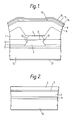
- a laser structure 1 according to an embodiment of the present invention comprises a layered mesa 2, 3, 4 buried by three confinement layers 5, 6, 7, a capping layer 8 and a contact layer 9.
- the lateral surfaces 10 of the mesa 2, 3, 4, against which the confinement layers 5, 6, 7 have been grown, are defined by (111) planes of the materials of the mesa 2, 3, 4.
- the resultant cross section of the mesa has a distinctive concertinalike appearance as a result.
- the laser structure 1 comprises a substrate 12 of (100) orientated S doped InP, doping level n approximately equal to 8 ⁇ 1018 cm ⁇ 3, about 250 ⁇ m thick. Covering the upper surface of the substrate 12 is a quaternary layer 11 of S doped GaInAsP (quaternary material), doping level n of the order of 1 to 2 ⁇ 1018 cm ⁇ 3, up to about 0.2 ⁇ m thick and of a band gap lying in the range from 1.0 to 1.3 ⁇ m.
- the layered mesa 2, 3, 4 is mounted on the quaternary material and has the following layers, starting with the lowermost:
- a capping layer 8 of Cd-doped InP Extending across the uppermost surfaces of both the mesa and the confinement layers 5, 6, 7 is a capping layer 8 of Cd-doped InP, doping level p approximately equal to 2 ⁇ 1018 cm ⁇ 3, of thickness lying in the range 1 to 2 ⁇ m.
- the capping layer 8 in turn is covered by a ternary contact layer 9 of Zn-doped GaInAs, doping level p approximately equal to 4 ⁇ 1019 cm ⁇ 3, of thickness lying in the range 0.05 to 0.3 ⁇ m.
- the contacts 15, 16 and 17 comprise Ti Au tunnelling Schottky contacts applied by radio frequency sputtering and annealing. Pt may advantageously be included as a diffusion barrier between the Ti and the Au in the contact 15, 16 through the window 13. This contact configuration is known and further details are not therefore provided herein.
- a double heterostructure wafer is produced.
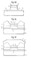
- the wafer (shown in Figure 2) comprises the substrate 12, the quaternary layer 11, and the layers 2, 3, 4 which are present in the mesa of the finished laser structure.
- the layers 11, 2, 3, 4 are all lattice-matched to the respective layer below, being grown by MOVPE under normal growth conditions.
- a silox stripe 18, 1.8 ⁇ m wide and 0.2 ⁇ m thick (shown in Figures 3a to 3e), is then produced extending in the (110) direction with respect to the crystalline structure of the substrate 12.
- the stripe 18 is produced by the use of the known combination of a positive photoresist mask and buffered HF as an etchant.
- Etching the wafer which comprises layers of different semi-conductor materials which must each be etched to produce the layered mesa 2, 3, 4, must be carried out using different selective etchants.
- the uppermost, InP layer 4 is etched using hydrobromic acid.
- the active layer 3 is etched using a mix of sulphuric acid, hydrogen peroxide and water.
- the InP buffer layer 2 is etched by again using hydrobromic acid. The actions of these etchants in this crystallographic orientation are well documented.
- the active layer 3 may be etched using a mixture of potassium dichromate (1/6 molar), sulphuric acid, and hydrochloric acid in the ratio 3 : 1 : 1. The action of this etchant is further discussed below.
- the hydrobromic acid etches through the uppermost InP layer 4 at a rate of about 6 ⁇ m per minute of InP at 20°C, or 2.5 ⁇ m per minute at 5°C, being stopped by the quaternary active layer 3.
- the etch rate drops significantly for instance by a factor of 3 or 4.
- the characteristic result at this stage is a shallow mesa profile with sides formed largely, or entirely, by (111) B planes. If the silox stripe 18 is well adhered to the InP layer 4, the planes exposed by the etchant are (111) A immediately below the silox stripe 18, then (111) B down to the active layer 3.
- the ratio of A to B planes (in terms of the depth of the mesa showing each type of plane at this stage) has been observed to be about 1 : 4. If the silox stripe 18 is not well adhered, then the only plane exposed is generally the (111) B plane.
- Figure 3b shows a mesa profile where the silox stripe 18 was not well adhered. In the latter case, as shown, there is a slight undercut, generally of up to 0.2 ⁇ m, of the silox stripe 18.
- hydrobromic acid contained colloidal particles. These were removed by filtration.
- the active layer 3 is then etched.
- the mixed etchant etches at a rate of 0.4 ⁇ m per minute and is stopped by the InP buffer layer 2.
- the sidewalls of the active layer 3 are characteristically etched to expose (111) A planes by this process. Hence at this stage a mesa has been formed which has an angular "bulge" in its sidewalls.
- the active layer 3 can alternatively be etched using a dichromate acid etchant.
- This etchant has the advantages of etching all wavelengths of quaternary material between InGaAs and InP, and of etching the active layer 3 only relatively slowly in a lateral direction once the (111) A plane has been exposed. Because of the latter feature, over etching of the active layer 3 does not cause deep undercutting of the uppermost InP layer 4. It has been found that the dichromate/acid etchant etches quaternary material of emission wavelength 1.5 ⁇ m at a rate of about 0.8 ⁇ m per minute in a downwards direction at 5°C.
- the etch time for the active layer 3 in the present case has been found to tend to be variable where there is lattice mismatch in the double heterostructure wafer.
- An etch time of 60 secs is used to ensure complete clearance of the active layer 3. (If the active layer 3 comprises a quaternary material having a band gap of 1.3 ⁇ m, then an etch time of 10 mins has been found suitable).
- the InP buffer layer 2 is then etched until the quaternary layer 11 which covers the substrate 12 stops the action of the etchant.
- the resultant layered mesa 2, 3, 4 has the characteristic concertinalike appearance referred to above. If the active layer 3 has been overetched, this final etching step has been found to cut the uppermost InP layer 4 back rapidly, but only as far as the top corner of the (111) A plane in the active layer 3. Hence the same mesa 2, 3, 4 profile is achieved, though the degree of overetching will affect the mesa width.
- the active layer 3 appears to act as a strongly adherent mask and the InP buffer layer 2 is at first etched along (111) A planes before the (111) B plane reasserts itself. This means that the angle produced in the mesa sidewall by the transition from A back to B planes does not coincide with the interface between the active and buffer layers 3, 2. This can be seen for instance in figure 3d.
- the three confinement layers 5, 6, 7 are grown in.
- the action of the silox stripe 18 during this stage is to suppress growth of InP. Referring to Figure 3e, the result is that the confinement layers 5, 6, 7 grow either side of the mesa leaving the silox stripe 18 exposed.
- Growth conditions for the confinement layers are generally as are normal for MOVPE growth but before growth starts, the sample is heated to 700°C for 20 minutes in the presence of PH3.
- This treatment has been found to enhance the action of the silox as a MOVPE growth-suppressing material even when the silox stripe is reduced in width for instance to values as low as about 1 um. Further, the heating involved appears to allow surface reconstruction to occur which improves the morphology of subsequently grown epitaxial layers. This surface reconstruction can be significant, modifying the lateral surfaces of the mesa by means of material transport particularly at the base of the mesa, and onto the exposed surfaces of the active layer.
- the concentration of PH3 should be high enough to prevent incongruous evaporation of the InP.
- the period for which the sample must be heated in the presence of PH3 will vary according to the conditions applied. For instance, if the concentration of PH3 is increased, the period may be reduced.
- the silox stripe is removed in a 40% aqueous solution of HF and the capping and contact layers 8, 9 are grown, again by MOVPE.
- the contacts 15, 16, 17 are applied by conventional techniques. It can then be conveniently mounted on a heat sink (not shown) by soldering the heat sink to the Au layer of the contact 15, 16.
- the confinement layers 5, 6, 7 tend to grow in substantially planar, particularly at a distance down the lateral surfaces of the mesa 2, 3, 4 of more than 0.5 ⁇ m from the silox stripe 18. Further, as mentioned above, the uppermost confinement layer 7 tends to "wing" away from the silox stripe 18, leaving a wide opening which gives good access for subsequent removal of the stripe 18.
- the capping and contact layers 8, 9 tend to grow with a planar characteristic which facilitates heat sinking and, also, at least two semiconductor junctions are grown by consecutive growth steps into the confinement layers 5, 6, 7. This avoids having junctions coincident with layer interfaces which have been chemically degraded for instance by the use of etchants.
- first quaternary layer 11 independent of the active layer 3, on the substrate 12. This acts as a stopping layer to the etchant used to etch the lowermost mesa layer 2. It also acts to prevent breakdown, even at large gate currents, of the p-n-p-n thyristor-like structure of the confinement layers 5, 6, 7 in combination with the capping layer 8. As a result leakage currents are blocked which would otherwise bypass the active region of the laser in use.
- a first quaternary layer 11 which is independent of the active layer 3, its characteristics such as band gap are not tied to those of the active layer 3. By reducing the bandgap, for instance to values in the range 1.0 to 1.3 ⁇ m as described above, the effectiveness of the first quaternary layer 11 in preventing leakage currents may then be improved.
- the first quaternary layer 11 has even a third function, as part of the waveguiding structure of the laser. As long as the buffer layer 2 of the mesa is sufficiently thin, the first quaternary layer 11 can "dilute" the lateral refractive index step at the sides of the mesa, allowing wider mesas with the same mode cut-off properties. This is desirable for processing, device resistance and radiation beam width reasons.
- the first quaternary layer 11 could have distributed feedback (DFB) gratings etched into it, planar growth being resumed to deposit the layers 2, 3 and 4 of the mesa. (Again the buffer layer 2 should be relatively thin, say from 0.1 to 0.5 ⁇ m thick, to allow the desired degree of optical interaction).
- DFB distributed feedback
- first quaternary layer in a semiconductor laser structure independent of the active layer, lying above the substrate and extending below the mesa, may be found advantageous more generally than in structures of the type described in the present specification.
- first quaternary layer 11 may be left out and a deeper buffer layer 2 used, the layered mesa 2, 3, 4 extending only partially down into the buffer layer 2.
- the final etching step, in which the buffer layer 2 is etched, will then have to be controlled by timing rather than by relying on the action of the first quaternary layer 11 as a stopping layer.
- FIG 6 it has been found advantageous to "notch" the active layer 3 immediately before heating and growth of the confinement layers.
- An etchant which attacks only the active layer 3, and which selectively exposes the (111) A planes, is used to narrow the active layer 3 preferentially.
- a suitable etchant comprises sulphuric acid, hydrogen peroxide, and water in the ratio 3:1:1. This "notching" of the active layer 3 is believed to provide a clean, fresh surface on the side of the active layer 3, which benefits the subsequent process steps.
- the unetched thickness of the buffer layer 2 may conveniently range up to 4 ⁇ m, and the height of the layered mesa 2, 3, 4 may be as much as 1.4 ⁇ m.
- Different dopants and doping levels may be used, such as Zn instead of Cd in the uppermost layer 4 of the mesa, doped to a level of 2 ⁇ 1018 cm ⁇ 3 instead of 5 ⁇ 1017 cm ⁇ 3.
- the second of the confinement layers 6 may comprise a "semi-insulating" material such as Fe doped InP instead of the p-doped InP referred to above. Such a material tends to have a relatively high resistivity.
- the silox stripe 18 might be replaced by a stripe of different material, such as a different form of silica, or another dielectric material such as Si3N4 or alumina.
- an additional p-doped layer 19 of InP may be grown onto the confinement layers 5, 6, 7. This avoids coincidence between the uppermost p-n junction provided by the confinement layers 5, 6, 7 and a chemically treated interface such as the interface between the confinement layers and the capping layer 8, which may be degraded during removal of the silox stripe 18.
- the uniformity of a plurality of mesas produced on a single wafer was investigated by taking a cleave from one end of the wafer and examining mesa dimensions using an SEM.
- the approximate size of the wafer was 10mm ⁇ 12mm. All of the mesa dimensions were found to have been controllable to within 0.1 ⁇ m.
- the wafer was subsequently overgrown with confinement layers and only an insignificant number of bridges of the silox stripes could be visually observed.
- Lasers fabricated according to embodiments of the present invention have produced up to 50 mW under direct current (dc) operation.
- the electrical characteristics have shown no appreciable conduction of current through the confinement layers due to mesa or overgrowth defects.
- far field spectra from such a laser have been found to show a full width at half maximum (fwhm) of 24° for the parallel direction and 30° for the perpendicular direction, with reference to the plane of the active layer.
- the far field spectra were also relatively smooth. It is considered that the smooth condition of the mesa sidewalls led to the smoothness of the far field spectra.
- the width of the active layer was measured in 80 different mesas, produced over five different wafers. Using silox stripes of 2.0 ⁇ m and 1.85 ⁇ m width, the active layer widths ranged from 1.4 ⁇ m to 1.9 ⁇ m, with one active layer width lying in the range from 1.9 ⁇ m to 2.0 ⁇ m.
- the active layer widths achieved on each wafer are shown as a histogram on Figure 11, differentiated as indicated by the markings within the columns of the histogram.
- semiconductor structures other than lasers can be fabricated as embodiments of the present invention.
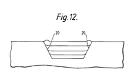
- a channel might be created, the sides 20 of the channel being provided by (111) B crystallographic planes. If material is subsequently grown into the channel in layers having a substantially flat characteristic almost right up to the sides 20 of the channel, then a particularly useful waveguiding structure can be created.
- the material grown into the channel may comprise a quaternary, InGaAsP, and the material into which the channel is created may comprises InP.
- optical detectors and opto-electronic integrated circuits are optical detectors and opto-electronic integrated circuits (OEICS).
Landscapes
- Physics & Mathematics (AREA)
- Geometry (AREA)
- Condensed Matter Physics & Semiconductors (AREA)
- General Physics & Mathematics (AREA)
- Electromagnetism (AREA)
- Optics & Photonics (AREA)
- Semiconductor Lasers (AREA)
- Bipolar Transistors (AREA)
- Led Devices (AREA)
- Thin Film Transistor (AREA)
- Recrystallisation Techniques (AREA)
- Pharmaceuticals Containing Other Organic And Inorganic Compounds (AREA)
- Semiconductor Memories (AREA)
Applications Claiming Priority (2)
| Application Number | Priority Date | Filing Date | Title |
|---|---|---|---|
| GB8622767 | 1986-09-22 | ||
| GB868622767A GB8622767D0 (en) | 1986-09-22 | 1986-09-22 | Semiconductor structures |
Publications (2)
| Publication Number | Publication Date |
|---|---|
| EP0261943A1 true EP0261943A1 (de) | 1988-03-30 |
| EP0261943B1 EP0261943B1 (de) | 1996-04-24 |
Family
ID=10604579
Family Applications (1)
| Application Number | Title | Priority Date | Filing Date |
|---|---|---|---|
| EP87308402A Expired - Lifetime EP0261943B1 (de) | 1986-09-22 | 1987-09-22 | Halbleiterstrukturen und deren Herstellungsverfahren |
Country Status (10)
| Country | Link |
|---|---|
| US (1) | US5242857A (de) |
| EP (1) | EP0261943B1 (de) |
| JP (1) | JP2708165B2 (de) |
| AT (1) | ATE137360T1 (de) |
| CA (1) | CA1332341C (de) |
| DE (1) | DE3751782T2 (de) |
| ES (1) | ES2085849T3 (de) |
| GB (1) | GB8622767D0 (de) |
| SG (1) | SG47931A1 (de) |
| WO (1) | WO1988002187A1 (de) |
Cited By (6)
| Publication number | Priority date | Publication date | Assignee | Title |
|---|---|---|---|---|
| GB2230383A (en) * | 1989-04-06 | 1990-10-17 | Electronic & Telecomm Res Inst | A method for manufacturing a buried heterostructure laser diode |
| EP0418953A1 (de) * | 1989-09-14 | 1991-03-27 | Koninklijke Philips Electronics N.V. | Verfahren zum Herstellen einer eine Mesa enthaltenden Halbleiteranordnung |
| FR2673330A1 (fr) * | 1991-02-26 | 1992-08-28 | France Telecom | Procede de realisation d'un laser a semiconducteur a ruban enterre, utilisant une gravure seche pour former ce ruban, et laser obtenu par ce procede. |
| EP0560491A1 (de) * | 1992-02-10 | 1993-09-15 | The Furukawa Electric Co., Ltd. | Halbleiterlaservorrichtung und Verfahren zur Herstellung |
| EP0664568A1 (de) * | 1994-01-21 | 1995-07-26 | Alcatel N.V. | Verfahren zur Herstellung eines segmentierten monokristallinen Wafers |
| DE4427840A1 (de) * | 1994-07-28 | 1996-02-01 | Osa Elektronik Gmbh | Verfahren zur Effizienzerhöhung von A¶I¶¶I¶¶I¶B¶V¶ - Halbleiter-Chips |
Families Citing this family (11)
| Publication number | Priority date | Publication date | Assignee | Title |
|---|---|---|---|---|
| JPH0831658B2 (ja) * | 1988-05-11 | 1996-03-27 | 三菱化学株式会社 | 半導体レーザ及びその製造方法 |
| US5568501A (en) * | 1993-11-01 | 1996-10-22 | Matsushita Electric Industrial Co., Ltd. | Semiconductor laser and method for producing the same |
| TW347597B (en) * | 1994-01-31 | 1998-12-11 | Mitsubishi Chem Corp | Method of forming a groove in a semiconductor laser diode and a semiconductor laser diode |
| US6036769A (en) * | 1994-06-29 | 2000-03-14 | British Telecommunications Public Limited Company | Preparation of semiconductor substrates |
| KR0146714B1 (ko) * | 1994-08-08 | 1998-11-02 | 양승택 | 평면 매립형 레이저 다이오드의 제조방법 |
| JP3765987B2 (ja) * | 2001-02-15 | 2006-04-12 | ユーディナデバイス株式会社 | 半導体装置の製造方法 |
| DE10305079B4 (de) * | 2002-11-27 | 2005-04-28 | Vertilas Gmbh | Verfahren zur Herstellung eines vergrabenen Tunnelkontakts in einem oberflächenemittierenden Halbleiterlaser sowie oberflächenemittierender Halbleiterlaser |
| JP5353113B2 (ja) | 2008-01-29 | 2013-11-27 | 豊田合成株式会社 | Iii族窒化物系化合物半導体の製造方法 |
| DE102018110187A1 (de) * | 2018-04-27 | 2019-10-31 | Osram Opto Semiconductors Gmbh | Optoelektronischer Halbleiterkörper, Anordnung von einer Vielzahl von optoelektronischen Halbleiterkörpern und Verfahren zur Herstellung eines optoelektronischen Halbleiterkörpers |
| JP7330128B2 (ja) * | 2020-04-02 | 2023-08-21 | 浜松ホトニクス株式会社 | 量子カスケードレーザ素子及び量子カスケードレーザ装置 |
| JP7421989B2 (ja) * | 2020-04-02 | 2024-01-25 | 浜松ホトニクス株式会社 | 量子カスケードレーザ素子及び量子カスケードレーザ装置 |
Citations (5)
| Publication number | Priority date | Publication date | Assignee | Title |
|---|---|---|---|---|
| US4276098A (en) * | 1980-03-31 | 1981-06-30 | Bell Telephone Laboratories, Incorporated | Batch processing of semiconductor devices |
| EP0039886A1 (de) * | 1980-05-09 | 1981-11-18 | Hitachi, Ltd. | Halbleiterlaser und Verfahren zu seiner Herstellung |
| DE3502326A1 (de) * | 1984-01-25 | 1985-08-01 | Hitachi, Ltd., Tokio/Tokyo | Licht emittierender chip und damit arbeitende optische kommunikationsvorrichtung |
| EP0188147A1 (de) * | 1984-12-11 | 1986-07-23 | Louis Menigaux | Verfahren zur Herstellung eines Halbleiterlasers mit vergrabener Streifenstruktur |
| WO1987000348A1 (en) * | 1985-07-03 | 1987-01-15 | British Telecommunications Public Limited Company | Semiconductor structures and a method of manufacturing semiconductor structures |
Family Cites Families (16)
| Publication number | Priority date | Publication date | Assignee | Title |
|---|---|---|---|---|
| US4371966A (en) * | 1980-11-06 | 1983-02-01 | Xerox Corporation | Heterostructure lasers with combination active strip and passive waveguide strip |
| GB2114808B (en) * | 1981-12-01 | 1985-10-09 | Standard Telephones Cables Ltd | Semiconductor laser manufacture |
| JPS58127392A (ja) * | 1982-01-25 | 1983-07-29 | Hitachi Ltd | 半導体レ−ザ−素子の製造方法 |
| GB2115608B (en) * | 1982-02-24 | 1985-10-30 | Plessey Co Plc | Semi-conductor lasers |
| US4509996A (en) * | 1982-11-05 | 1985-04-09 | International Standard Electric Corporation | Injection laser manufacture |
| JPS59181589A (ja) * | 1983-03-31 | 1984-10-16 | Fujitsu Ltd | 半導体レ−ザの製造方法 |
| EP0157555B1 (de) * | 1984-03-27 | 1990-10-03 | Matsushita Electric Industrial Co., Ltd. | Halbleiterlaser und Verfahren zu dessen Fabrikation |
| US4595454A (en) * | 1984-06-15 | 1986-06-17 | At&T Bell Laboratories | Fabrication of grooved semiconductor devices |
| US4660208A (en) * | 1984-06-15 | 1987-04-21 | American Telephone And Telegraph Company, At&T Bell Laboratories | Semiconductor devices employing Fe-doped MOCVD InP-based layer for current confinement |
| US4888624A (en) * | 1984-06-15 | 1989-12-19 | American Telephone And Telegraph Company, At&T Bell Laboratories | Semiconductor devices employing high resistivity in-based compound group III-IV epitaxial layer for current confinement |
| JP2716693B2 (ja) * | 1985-02-08 | 1998-02-18 | ソニー株式会社 | 半導体レーザー |
| JPS62245691A (ja) * | 1986-04-17 | 1987-10-26 | Nec Corp | 半導体レ−ザの製造方法 |
| US4788159A (en) * | 1986-09-18 | 1988-11-29 | Eastman Kodak Company | Process for forming a positive index waveguide |
| US4701995A (en) * | 1986-10-29 | 1987-10-27 | American Telephone And Telegraph Company, At&T Bell Laboratories | Method of making a nonplanar buried-heterostructure distributed-feedback laser |
| US4774554A (en) * | 1986-12-16 | 1988-09-27 | American Telephone And Telegraph Company, At&T Bell Laboratories | Semiconductor devices employing Ti-doped Group III-V epitaxial layer |
| JPH0646669B2 (ja) * | 1987-07-28 | 1994-06-15 | 日本電気株式会社 | 半導体レ−ザ及びその製造方法 |
-
1986
- 1986-09-22 GB GB868622767A patent/GB8622767D0/en active Pending
-
1987
- 1987-09-22 DE DE3751782T patent/DE3751782T2/de not_active Expired - Lifetime
- 1987-09-22 JP JP62505541A patent/JP2708165B2/ja not_active Expired - Lifetime
- 1987-09-22 CA CA000547521A patent/CA1332341C/en not_active Expired - Lifetime
- 1987-09-22 AT AT87308402T patent/ATE137360T1/de not_active IP Right Cessation
- 1987-09-22 ES ES87308402T patent/ES2085849T3/es not_active Expired - Lifetime
- 1987-09-22 WO PCT/GB1987/000667 patent/WO1988002187A1/en not_active Ceased
- 1987-09-22 EP EP87308402A patent/EP0261943B1/de not_active Expired - Lifetime
- 1987-09-22 SG SG1996005448A patent/SG47931A1/en unknown
-
1992
- 1992-01-22 US US07/824,869 patent/US5242857A/en not_active Expired - Lifetime
Patent Citations (5)
| Publication number | Priority date | Publication date | Assignee | Title |
|---|---|---|---|---|
| US4276098A (en) * | 1980-03-31 | 1981-06-30 | Bell Telephone Laboratories, Incorporated | Batch processing of semiconductor devices |
| EP0039886A1 (de) * | 1980-05-09 | 1981-11-18 | Hitachi, Ltd. | Halbleiterlaser und Verfahren zu seiner Herstellung |
| DE3502326A1 (de) * | 1984-01-25 | 1985-08-01 | Hitachi, Ltd., Tokio/Tokyo | Licht emittierender chip und damit arbeitende optische kommunikationsvorrichtung |
| EP0188147A1 (de) * | 1984-12-11 | 1986-07-23 | Louis Menigaux | Verfahren zur Herstellung eines Halbleiterlasers mit vergrabener Streifenstruktur |
| WO1987000348A1 (en) * | 1985-07-03 | 1987-01-15 | British Telecommunications Public Limited Company | Semiconductor structures and a method of manufacturing semiconductor structures |
Non-Patent Citations (3)
| Title |
|---|
| APPLIED PHYSICS LETTERS, vol. 44, no. 10, 15th May 1984, pages 975-977, American Institute of Physics, New York, US; K. IMANAKA et al.: "A novel technique to fabricate GaInAsP/InP buried heterostructure laser diodes" * |
| APPLIED PHYSICS LETTERS, vol. 46, no. 2, 15th January 1985, pages 131-133, American Institute of Physics, New York, US; M. RAZEGHI et al.: "Very low threshold buried ridge structure lasers emitting at 1.3 mum grown by low pressure metalorganic chemical vapor deposition" * |
| IEEE JOURNAL OF QUANTUM ELECTRONICS, vol. QE-17, no. 5, May 1981, pages 640-645, IEEE, New York, US; S. ARAI et al.: "1.6 mum wavelength GaInAsP/InP BH lasers" * |
Cited By (11)
| Publication number | Priority date | Publication date | Assignee | Title |
|---|---|---|---|---|
| GB2230383A (en) * | 1989-04-06 | 1990-10-17 | Electronic & Telecomm Res Inst | A method for manufacturing a buried heterostructure laser diode |
| GB2230383B (en) * | 1989-04-06 | 1993-01-20 | Elect & Telecomm Research Inst | A method for manufacturing a buried heterostructure laser diode |
| EP0418953A1 (de) * | 1989-09-14 | 1991-03-27 | Koninklijke Philips Electronics N.V. | Verfahren zum Herstellen einer eine Mesa enthaltenden Halbleiteranordnung |
| FR2673330A1 (fr) * | 1991-02-26 | 1992-08-28 | France Telecom | Procede de realisation d'un laser a semiconducteur a ruban enterre, utilisant une gravure seche pour former ce ruban, et laser obtenu par ce procede. |
| EP0501862A1 (de) * | 1991-02-26 | 1992-09-02 | France Telecom | Verfahren zur Herstellung eines Halbleiterlasers mit vergrabener Streifenstruktur unter Verwendung von Trockenätzen zur Herstellung dieses Streifens und ein nach diesem Verfahren hergestellter Laser |
| US5304283A (en) * | 1991-02-26 | 1994-04-19 | France Telecom Etablissment Autonome De Droit Public | Process for producing a buried stripe semiconductor laser using dry etching for forming said stripe and laser obtained by this process |
| EP0560491A1 (de) * | 1992-02-10 | 1993-09-15 | The Furukawa Electric Co., Ltd. | Halbleiterlaservorrichtung und Verfahren zur Herstellung |
| EP0664568A1 (de) * | 1994-01-21 | 1995-07-26 | Alcatel N.V. | Verfahren zur Herstellung eines segmentierten monokristallinen Wafers |
| FR2715506A1 (fr) * | 1994-01-21 | 1995-07-28 | Alcatel Nv | Procédé de remplacement d'une partie d'une première structure semi-conductrice par une autre structure semi-conductrice comportant une couche épitaxiale de composition différente. |
| US5646064A (en) * | 1994-01-21 | 1997-07-08 | Alcatel N.V. | Method of fabricating a segmented monocrystalline chip |
| DE4427840A1 (de) * | 1994-07-28 | 1996-02-01 | Osa Elektronik Gmbh | Verfahren zur Effizienzerhöhung von A¶I¶¶I¶¶I¶B¶V¶ - Halbleiter-Chips |
Also Published As
| Publication number | Publication date |
|---|---|
| US5242857A (en) | 1993-09-07 |
| EP0261943B1 (de) | 1996-04-24 |
| CA1332341C (en) | 1994-10-11 |
| JP2708165B2 (ja) | 1998-02-04 |
| ATE137360T1 (de) | 1996-05-15 |
| DE3751782T2 (de) | 1996-09-05 |
| SG47931A1 (en) | 1998-04-17 |
| ES2085849T3 (es) | 1996-06-16 |
| WO1988002187A1 (en) | 1988-03-24 |
| JPH01501586A (ja) | 1989-06-01 |
| DE3751782D1 (de) | 1996-05-30 |
| GB8622767D0 (en) | 1986-10-29 |
Similar Documents
| Publication | Publication Date | Title |
|---|---|---|
| EP0227783B1 (de) | Verfahren zur herstellung von optischen halbleiterstrukturen | |
| EP0261943B1 (de) | Halbleiterstrukturen und deren Herstellungsverfahren | |
| US5082799A (en) | Method for fabricating indium phosphide/indium gallium arsenide phosphide buried heterostructure semiconductor lasers | |
| US5390205A (en) | Semiconductor laser | |
| JPH0775267B2 (ja) | 半導体装置及びその製造プロセス | |
| EP0114109B1 (de) | Halbleiterlaser-Vorrichtung und Verfahren zu deren Herstellung | |
| EP0695007A1 (de) | Halbleitervorrichtung und Herstellungsverfahren | |
| US7184640B2 (en) | Buried heterostructure device fabricated by single step MOCVD | |
| US6639926B1 (en) | Semiconductor light-emitting device | |
| US5222091A (en) | Structure for indium phosphide/indium gallium arsenide phosphide buried heterostructure semiconductor | |
| JPH07254750A (ja) | 半導体レーザ | |
| HK111597A (en) | Semiconductor structures and a method of manufacturing semiconductor structures | |
| US5674779A (en) | Method for fabricating a ridge-shaped laser in a channel | |
| JP3132054B2 (ja) | 埋込み構造半導体レーザの製造方法 | |
| EP0255344A1 (de) | Herstellungstechnik einer Halbleiterstruktur | |
| DE4240539A1 (en) | Semiconductor device mfr. e.g. for ridge waveguide semiconductor laser prodn. | |
| JPH084172B2 (ja) | 埋め込み型量子井戸半導体レーザ | |
| Takemi et al. | MOCVD regrowth of InP on RIE patterned substrates for p-substrate 1.3/spl mu/m BH laser application | |
| JPS63236384A (ja) | 半導体レ−ザの製造方法 | |
| GB2299706A (en) | Semiconductor laser and method of manufacture | |
| JPH06152065A (ja) | 半導体発光素子及びその製造方法 | |
| JPH03125489A (ja) | 半導体レーザ装置の製造方法 |
Legal Events
| Date | Code | Title | Description |
|---|---|---|---|
| PUAI | Public reference made under article 153(3) epc to a published international application that has entered the european phase |
Free format text: ORIGINAL CODE: 0009012 |
|
| AK | Designated contracting states |
Kind code of ref document: A1 Designated state(s): AT BE CH DE ES FR GB GR IT LI LU NL SE |
|
| 17P | Request for examination filed |
Effective date: 19880921 |
|
| 17Q | First examination report despatched |
Effective date: 19900924 |
|
| GRAH | Despatch of communication of intention to grant a patent |
Free format text: ORIGINAL CODE: EPIDOS IGRA |
|
| GRAA | (expected) grant |
Free format text: ORIGINAL CODE: 0009210 |
|
| AK | Designated contracting states |
Kind code of ref document: B1 Designated state(s): AT BE CH DE ES FR GB GR IT LI LU NL SE |
|
| PG25 | Lapsed in a contracting state [announced via postgrant information from national office to epo] |
Ref country code: AT Effective date: 19960424 Ref country code: GR Free format text: LAPSE BECAUSE OF FAILURE TO SUBMIT A TRANSLATION OF THE DESCRIPTION OR TO PAY THE FEE WITHIN THE PRESCRIBED TIME-LIMIT Effective date: 19960424 |
|
| REF | Corresponds to: |
Ref document number: 137360 Country of ref document: AT Date of ref document: 19960515 Kind code of ref document: T |
|
| ITF | It: translation for a ep patent filed | ||
| REF | Corresponds to: |
Ref document number: 3751782 Country of ref document: DE Date of ref document: 19960530 |
|
| REG | Reference to a national code |
Ref country code: ES Ref legal event code: FG2A Ref document number: 2085849 Country of ref document: ES Kind code of ref document: T3 |
|
| ET | Fr: translation filed | ||
| PG25 | Lapsed in a contracting state [announced via postgrant information from national office to epo] |
Ref country code: LU Free format text: LAPSE BECAUSE OF NON-PAYMENT OF DUE FEES Effective date: 19960930 |
|
| PLBE | No opposition filed within time limit |
Free format text: ORIGINAL CODE: 0009261 |
|
| STAA | Information on the status of an ep patent application or granted ep patent |
Free format text: STATUS: NO OPPOSITION FILED WITHIN TIME LIMIT |
|
| 26N | No opposition filed | ||
| PGFP | Annual fee paid to national office [announced via postgrant information from national office to epo] |
Ref country code: NL Payment date: 19980819 Year of fee payment: 12 |
|
| PGFP | Annual fee paid to national office [announced via postgrant information from national office to epo] |
Ref country code: BE Payment date: 19980904 Year of fee payment: 12 |
|
| PGFP | Annual fee paid to national office [announced via postgrant information from national office to epo] |
Ref country code: ES Payment date: 19980907 Year of fee payment: 12 |
|
| PG25 | Lapsed in a contracting state [announced via postgrant information from national office to epo] |
Ref country code: ES Free format text: LAPSE BECAUSE OF NON-PAYMENT OF DUE FEES Effective date: 19990923 |
|
| PG25 | Lapsed in a contracting state [announced via postgrant information from national office to epo] |
Ref country code: BE Free format text: LAPSE BECAUSE OF NON-PAYMENT OF DUE FEES Effective date: 19990930 |
|
| BERE | Be: lapsed |
Owner name: BRITISH TELECOMMUNICATIONS P.L.C. Effective date: 19990930 |
|
| PG25 | Lapsed in a contracting state [announced via postgrant information from national office to epo] |
Ref country code: NL Free format text: LAPSE BECAUSE OF NON-PAYMENT OF DUE FEES Effective date: 20000401 |
|
| NLV4 | Nl: lapsed or anulled due to non-payment of the annual fee |
Effective date: 20000401 |
|
| REG | Reference to a national code |
Ref country code: GB Ref legal event code: 732E |
|
| REG | Reference to a national code |
Ref country code: GB Ref legal event code: IF02 |
|
| REG | Reference to a national code |
Ref country code: ES Ref legal event code: FD2A Effective date: 20001013 |
|
| REG | Reference to a national code |
Ref country code: CH Ref legal event code: NV Representative=s name: JACOBACCI & PERANI S.A. |
|
| PGFP | Annual fee paid to national office [announced via postgrant information from national office to epo] |
Ref country code: FR Payment date: 20060810 Year of fee payment: 20 |
|
| PGFP | Annual fee paid to national office [announced via postgrant information from national office to epo] |
Ref country code: GB Payment date: 20060811 Year of fee payment: 20 |
|
| PGFP | Annual fee paid to national office [announced via postgrant information from national office to epo] |
Ref country code: DE Payment date: 20060815 Year of fee payment: 20 Ref country code: CH Payment date: 20060815 Year of fee payment: 20 |
|
| PGFP | Annual fee paid to national office [announced via postgrant information from national office to epo] |
Ref country code: IT Payment date: 20060930 Year of fee payment: 20 |
|
| REG | Reference to a national code |
Ref country code: CH Ref legal event code: PL |
|
| REG | Reference to a national code |
Ref country code: GB Ref legal event code: PE20 |
|
| EUG | Se: european patent has lapsed | ||
| PG25 | Lapsed in a contracting state [announced via postgrant information from national office to epo] |
Ref country code: GB Free format text: LAPSE BECAUSE OF EXPIRATION OF PROTECTION Effective date: 20070921 |
|
| PGFP | Annual fee paid to national office [announced via postgrant information from national office to epo] |
Ref country code: SE Payment date: 20060818 Year of fee payment: 20 |