EP0262468A2 - Dispositif de mémoire fifo reconfigurable - Google Patents
Dispositif de mémoire fifo reconfigurable Download PDFInfo
- Publication number
- EP0262468A2 EP0262468A2 EP87113044A EP87113044A EP0262468A2 EP 0262468 A2 EP0262468 A2 EP 0262468A2 EP 87113044 A EP87113044 A EP 87113044A EP 87113044 A EP87113044 A EP 87113044A EP 0262468 A2 EP0262468 A2 EP 0262468A2
- Authority
- EP
- European Patent Office
- Prior art keywords
- data
- storage means
- words
- locations
- providing
- Prior art date
- Legal status (The legal status is an assumption and is not a legal conclusion. Google has not performed a legal analysis and makes no representation as to the accuracy of the status listed.)
- Ceased
Links
Images




Classifications
-
- G—PHYSICS
- G06—COMPUTING OR CALCULATING; COUNTING
- G06F—ELECTRIC DIGITAL DATA PROCESSING
- G06F5/00—Methods or arrangements for data conversion without changing the order or content of the data handled
- G06F5/06—Methods or arrangements for data conversion without changing the order or content of the data handled for changing the speed of data flow, i.e. speed regularising or timing, e.g. delay lines, FIFO buffers; over- or underrun control therefor
- G06F5/065—Partitioned buffers, e.g. allowing multiple independent queues, bidirectional FIFO's
-
- G—PHYSICS
- G06—COMPUTING OR CALCULATING; COUNTING
- G06F—ELECTRIC DIGITAL DATA PROCESSING
- G06F2205/00—Indexing scheme relating to group G06F5/00; Methods or arrangements for data conversion without changing the order or content of the data handled
- G06F2205/06—Indexing scheme relating to groups G06F5/06 - G06F5/16
- G06F2205/066—User-programmable number or size of buffers, i.e. number of separate buffers or their size can be allocated freely
-
- G—PHYSICS
- G06—COMPUTING OR CALCULATING; COUNTING
- G06F—ELECTRIC DIGITAL DATA PROCESSING
- G06F2205/00—Indexing scheme relating to group G06F5/00; Methods or arrangements for data conversion without changing the order or content of the data handled
- G06F2205/06—Indexing scheme relating to groups G06F5/06 - G06F5/16
- G06F2205/067—Bidirectional FIFO, i.e. system allowing data transfer in two directions
Definitions
- This invention relates to first-in-first-out (FIFO) memory devices and more specifically to FIFO memories which facilitate data communication between a host CPU and a peripheral device.
- FIFO first-in-first-out
- FIFO memories it is known in the art to use FIFO memories to facilitate data communication between a host CPU and a peripheral device.
- U.S. Patent 4,145,755 issued to Suzuki et al. discusses a system in which a CPU loads a FIFO memory with data. After the FIFO memory is filled with data, the data in the FIFO memory is transferred to a peripheral device.
- the Suzuki FIFO memory device provides flag signals to the host CPU indicating when the FIFO memory is full or empty.
- the system discussed in the ⁇ 755 patent is relatively simple and only allows for data to be transferred from the host CPU to the peripheral device.
- FIG. 2 of the ⁇ 732 patent Another type of FIFO memory is illustrated in Figure 2 of the ⁇ 732 patent.
- the FIFO memory of Figure 2 includes a RAM which is addressed by a first up-down counter during transfer of data between a host CPU and the RAM. The contents of the first up-down counter can be preset to any desired value by the host CPU.
- the RAM is also addressed by a second up-down counter during transfer of data between a peripheral device and the RAM. The second up-down counter can be preset to any desired value by the peripheral device.
- the FIFO memory can pass information from the host CPU to the peripheral device or from the peripheral device to the host CPU.
- a FIFO memory device constructed in accordance with my invention facilitates communication of data between a host CPU and a peripheral device.
- the FIFO memory device includes first and second RAMs which can be configured to function in a number of modes in response to commands from the host CPU.
- the first RAM serves as a FIFO memory which receives data from the host CPU and provides that data on a first-in-first-out basis to the peripheral device while the second RAM receives data from the peripheral device and provides that data on a first-in-first-out basis to the host CPU.
- the host CPU can selectively address any desired location within either the first or second RAM and either read data from or write data to that location. In this way, the host CPU can write data to or retrieve data from the FIFO memory device without having to wait for location pointers within the FIFO memory device to reach a desired address.
- the first and second RAMs can also be configured to act as a single FIFO memory device to either pass data from the host CPU to the peripheral device or pass data from the peripheral device to the host CPU.
- the FIFO memory can be commanded by the host CPU to provide data stored in a specific block of addresses from the first RAM to the peripheral device or load data from the peripheral device into a specific block of addresses in the second RAM.
- the FIFO memory can be programmed to store data from the host CPU into a specific block of addresses within the first RAM or provide data from a specific block of addresses within the second RAM to the host CPU.
- the FIFO memory can also be commanded to function in a number of modes which are variations of the above-described modes. It will be appreciated therefore that the FIFO memory device of the present invention can be used in a large number of applications to fulfill a variety of requirements.
- the first and second RAMs are each organized into columns and rows of addresses, and are each addressed by an associated pair of counters.
- the first counter within the pair is a binary counter which selects a column while the second counter selects a row.
- the RAMs are typically large, e.g. 8 columns and 128 rows for a total of 1,024 locations.
- a first ring counter is used to select a row within each RAM and a second ring counter is used to select a column within each RAM.
- a plurality of ring counters is used to select a row.
- three four bit ring counters and a two bit ring counter are used to select one of the 128 rows. Because the surface area of an integrated circuit including the four ring counters is smaller than the surface area used to provide a 128-bit ring counter, the FIFO memory of the present invention is less expensive to manufacture than a device using a single 128-bit ring counter.
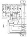
- FIG. 1 is a block diagram of FIFO memory device 10 constructed in accordance with one embodiment of my invention.
- Memory device 10 includes a first port 12 for transferring data between memory device 10 and a host CPU 14.
- device 10 includes a bidirectional data bus 12a and an address bus 12b coupled to port 12.
- Host CPU 14 can be any of a number of devices, e.g. a conventional microprocessor.
- Memory device 10 also includes a port 16 for communicating with a device 18.
- Device 18 can be any of a number of devices, e.g. a peripheral device such as a magnetic disk or any other digital device capable of transferring data.
- memory device 10 facilitates communication of data between host CPU 14 and device 18.
- Memory device 10 can operate in any of a number of modes. In a first set of modes, data is provided by host CPU 14 to memory device 10 which is then read by device 18. Similarly, device 18 also provides data to memory device 10 which is read by host CPU 14. In a second set of modes, data transfer is only in a single direction, i.e. from host CPU 14 to device 18 via memory device 10 or from device 18 to host CPU 14 via memory device 10. These modes are discussed in detail below. Host CPU 14 selects the mode that memory device 10 operates in by writing a word of data into a control register 19 within device 10, as will be discussed in detail below.
- Memory device 14 includes first and second dual port RAMs 20a and 20b.
- RAMs 20a and 20b each store 1,024 words of data, each word including 9 bits. (The ninth bit of each word in RAMS 20a and 20b is typically used as a parity bit.)
- RAM 20a serves as a first FIFO memory which receives words of data from host CPU14 via data bus 12a and provides those words on a first-in-first-out basis to device 18 via an output bus 21a, a multiplexer 17b and a data bus 16a coupled to port 16.
- RAM 20b acts as a second FIFO memory which receives words of data from device 18 via data bus 16a provides those words on a first-in-first-out basis to host CPU 14 via a bus 23b, a multiplexer 17a, and data bus 12a.
- RAM 20a is addressed by a write counter 24w via a multiplexer 30. Each time a word is transferred from host CPU 14 to dual port RAM 20a, write counter 24w increments. In this way, successive words of data from host CPU 14 are loaded into successive locations within RAM 20a.
- RAM 20a is addressed by a read counter 24r via a multiplexer 33. As words of data are read from RAM 20a by device 18, read counter 24r increments. Device 18 therefore reads data stored in successive locations of dual port RAM 20a. In this way, RAM 20a provides data from host CPU 14 to device 18 on a first-in-first-out basis.
- dual port RAM 20b also acts as a FIFO memory which receives data from device 18.
- dual port RAM 20b is addressed by a write counter 26w via a multiplexer 34. Each time a word of data is transferred from device 18 to dual port RAM 20b, write counter 26w increments.
- host CPU 14 receives data from dual port RAM 20b, dual port RAM 20b is addressed by a read counter 26r via a multiplexer 31. Each time host CPU 14 receives a word of data from device 10, read counter 26r increments. In this way, host CPU 14 receives data from successive locations in dual port RAM 20b.
- dual port RAM 20a can also be addressed directly by host CPU 14.
- host CPU 14 stores a desired address in an address register 28 (via address bus 12b) which addresses RAM 20a via multiplexer 30 during write operations and via multiplexer 33 during read operations.
- address register 28 can also be used to address any location within dual port RAM 20b via multiplexer 31 during read operations and via multiplexer 34 during write operations.
- Host CPU 14 can therefore write data to or receive data from any location in dual port RAM 20b, regardless of the order in which that data was written. Therefore, if it is desired to read data from or write data to a specific location in RAM 20a or 20b, it is not necessary to wait for counter 24w, 24r, 26w, or 26r to increment to that address.
- Memory device 10 includes circuit 27a which compares the contents of read counter 24r and write counter 24w and provides output signals FULL1 and EMPTY1 when RAM 20a is full and empty, respectively.
- Signal FULL1 is provided to host CPU 14 and peripheral device 18 via a multiplexer 29a and a lead 71.
- Signal EMPTY1 is provided to host CPU 14 and peripheral device 18 via a lead 72. If host CPU 14 performs 1,024 more write operations than the number of read operations performed by peripheral device 18, signal FULL1 goes active (high). Host CPU 14 typically responds to signal FULL1 by ceasing further write operations until signal FULL1 goes low. Similarly, when the number of write operations performed by host CPU 14 equals the number of read operations performed by peripheral device 18, signal EMPTY1 goes active.
- Peripheral device 18 typically responds to signal EMPTY1 by ceasing further read operations until signal EMPTY1 goes low.
- Signals FULL2 and EMPTY2 provide similar information regarding the status of RAM 20b.
- Signal FULL2 is provided by a circuit 27b via a multiplexer 29b and a lead 73.
- Signal EMPTY2 is provided by circuit 27b to host CPU 14 and peripheral device 18 via a lead 74.
- RAMs 20a and 20b are configured to function as a single 2,048 word FIFO memory device.
- data from host CPU 14 is written into successive locations of dual port RAM 20a via data bus 12a.
- dual port RAM 20a is addressed by write counter 24w.
- the next word of data from host CPU 14 is loaded into the first location of dual port RAM 20b, which is addressed by write counter 26w.
- Successive words of data from host CPU 14 are thereafter loaded into successive locations in dual port RAM 20b.
- the next word of data from host CPU 14 is stored in the first location of dual port RAM 20a.
- device 18 receives words of data stored in successive locations within dual port RAM 20a.
- dual port RAM 20a is addressed by read counter 24r. After data from the last location of dual port RAM 20a is read by device 18, upon the next request for data by device 18, the word of data located in the first location of dual port RAM 20b if provided to device 18.
- dual port RAM 20b is addressed by read counter 26r. In this way, dual port RAMs 20a and 20b function as a single 2Kx9 FIFO memory which recieves data from host CPU 14 and provides that data to device 18.
- memory device 10 provides signals FULL1, EMPTY1, FULL2 and EMPTY2 when RAM 20a is full, when RAM 20a is empty, when RAM 20b is full, and when RAM 20b is empty, respectively.
- Signals FULL1, EMPTY1, FULL2 and EMPTY2 are received by host CPU 14 and processed in a manner dependent on the program being executed by host CPU 14.
- host CPU 14 can access any location in either RAM 20a or RAM 20b to either read data or write data. This is done by storing an address in address register 28 as described above.
- Single FIFO mode B is identical to single FIFO mode A, except memory device 10 receives data from device 18 and provides that data on a first-in-first-out basis to host CPU 14.
- RAMs 20a and 20b are addressed by write counters 24w and 26w, respectively.
- RAMs 20a and 20b are addressed by read counters 24r and 26r, respectively.
- host CPU 14 can access any location in RAM 20a or 20b and either read from or write data to that location.
- either port 12 or port 16 or both ports 12 and 16 can function in DMA mode.
- the DMA mode can best be understood by example.
- device 10 is in the dual FIFO mode
- host CPU 14 determines that port 16 is in the DMA mode
- device 18 transfers a predetermined number of words to memory device 10. These words are stored in a predetermined block of addresses within RAM 20b.
- Host CPU 14 determines that the first word of data from device 18 will be stored, for example, at location 20 within RAM 20b and the last word will be at location 39 in RAM 20b. Host CPU 14 loads the value 20 in counter 26w and the value 39 in a register EOC3. In addition, in this example, host CPU 14 programs device 10 to provide an output signal AF2 to host CPU 14 and device 18 to indicate when 15 words of data have been stored in RAM 20b by device 18. Accordingly, host CPU 14 loads the value 35 (20 + 15) into a register FLAG3. As successive words of data are loaded into RAM 20b by device 18, the contents of counter 26w increment.
- locations 20, 35, and 39 are merely exemplary and that other addresses can be selected by host CPU 14.
- Device 10 also includes registers EOC1, EOC2, EOC4, FLAF1, FLAG2 and FLAG4, which are also used during DMA operations. These registers function as indicated below.
- device 10 includes a 12-bit address bus 12b which receives addresses from host CPU 14. Of importance, an address line A11 of bus 12b indicates to device 10 whether host CPU 14 is attempting to access one of the registers listed in TABLE I or a location within one of RAMs 20a and 20b.
- RAMs 20a and 20b each include 1024 locations for a total of 2,048 locations, a 10-bit address is required to select a location in RAMs 20a and 20b.
- data bus 12a transmits 9 bits of data between host CPU 14 and RAMs 20a and 20b, as mentioned above, the ninth bit of bus 12a typically transmits a parity signal. This ninth bit of bus 12a is therefore not received by the registers listed in TABLE I.
- each register FLAG1 to FLAG4, EOC1 to EOC4, and counters 24r, 24w, 26r and 26w are each mapped into two locations as indicated below, one location for receiving the lower eight bits and one location for receiving the higher two bits.
- counters 24w, 24r, 26w and 26r can be read by host CPU 14 via buffers 39a, 39b, 39c, and 39d, respectively, by way of data bus 12a.
- Control register 19 controls the mode of operation for device 10.
- the bit definition for control register 19 is as follows:
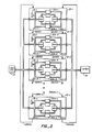
- device 10 can be cascaded with one or more memory devices identical to device 10 so that the cascaded memory devices function as two nKx9 FIFO memory devices where n is the number of devices cascaded together.
- memory devices 10-1 to 10-n receive data from host CPU 14 and provide that data on a first-in-first-out basis to device 18.
- memory devices 10-1 to 10-n receive data from peripheral device 18 and provide that data on a first-in-first-out basis to host CPU 14.
- Memory device 10-1 provides output signals ABXO1 and BAXO1 to device 10-2, device 10-2 provides signals ABXO2 and BAKO2 to device 10-3, and so on.
- Device 10-n provides signals ABXOn and BAXOn to device 10-1. As described below, signals ABXO1 to ABXOn and BAKO1 to BAXOn determine which memory device 10-1 to 10-n stores data from host CPU 14, which memory device 10-1 to 10-n stores data from peripheral device 18, which memory device 10-1 to 10-n provides data to host CPU 14, and which memory device 10-1 to 10-n provides data to peripheral device 18.
- memory devices 10-1 to 10-n are initialized by writing an appropriate word of data to control registers 19-1 to 19-n, respectively. Specifically, bit 2 of control register 19-1 is set to zero and bit 2 of control registers 19-2 to 19-n is set to one. Because of this, signals ABXO1 to ABXOn and BAXO1 to BAXOn are set to zero. Also, because bit 2 of control register 19-1 is set to zero, as data is provided to memory devices 10-1 to 10-n by host CPU 14, that data is stored in successive locations within RAM 20a-1 of device 10-1.
- signal ABXO1 goes high, indicating that subsequent words of data provided to memory devices 10-1 to 10-n are to be stored in RAM 20a-2 of memory device 10-2.
- signal ABXO2 goes high. Data subsequently provided by host CPU 14 is stored in RAM 20a-3 of memory device 10-3.
- RAM 20a-1 of device 10-1 provides that data.
- signal ABXO1 goes low.
- peripheral device 19 again attempts to read data from memory devices 10-1 to 10-n, that data is provided by RAM 20a-2 of device 10-2. In this way, RAMS 20a-1 to 20a-n act as a single nKx9 FIFO memory device.
- Signals BAXO1 to BAXOn function in a manner similar to signals ABXO1 to ABXOn to control flow of information to and from RAMs 20b-1 to 20b-n.
- Figure 2 illustrates serially cascaded memory devices.
- a plurality of FIFO memory devices such as device 10 can also be connected in parallel to permit storage of wider words.
- two memory devices can be coupled to form a first 1K x 18 FIFO memory for transferring data from host CPU 14 to peripheral device 18 and a second 1K x 18 FIFO memory for transferring data from peripheral device 18 to host CPU 14.
- counters 24r, 24w, 26r, and 26w each comprise a binary counter.
- counters 24r, 24w, 26r, and 26w each comprise a set of ring counters.
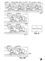
- FIG. 3 is a block diagram of an embodiment of counter 24w in which counter 24w comprises a set of ring counters, it being understood that counters 24r, 26w and 26r are identical to counter 24w.
- counter 24w actually comprises five ring counters 100a to 100e.
- a decoder 102 selects a row in response to the state of ring counters 100b to 100e.
- ring counter 100b has four possible states corresponding to which one of four output leads 100b-1 to 100b-4 is in a high state.
- ring counter 100c has four possible states
- ring counter 100d has two possible states
- ring counter 100e has four possible states.
- there are 128 (4x4x2x4) possible permutations of states for counters 100b to 100e and thus, counters 100b to 100e determine which of the 128 rows within RAM 20a is selected by decoder 102.
- Decoder 102 receives the signals on leads 100b-1 to 100b-4, 100c-1 to 100c-4, 100d-1 to 100d-2, and 100e-1 to 100e-4, from ring counters 100b to 100e and provides a select signal on one of 128 output leads 102-1 to 102-128 in response thereto.
- a circuit constructed in accordance with my invention can be formed on a smaller surface area of an integrated circuit, and is therefore less expensive to build. It will be appreciated, however, that in other embodiments, different numbers of ring counters with different numbers of stages can be used to address RAM locations.
- Ring counter 100a changes state each time counter 24w addresses dual port RAM 20a.
- the last output lead 100a-8 of ring counter 100a is high, the next time counter 24w addresses dual port RAM 20a, last output lead 100a-8 of counter 100a goes low, first output lead 100a-1 of ring counter 100a goes high, and ring counter 100b changes state.
- ring counter 100c only changes state when last output lead 100a-8 of ring counter 100a and last output lead 100b-4 of ring counter 100b are both high. Ring counters 100d and 100e change state in a similar manner.
- counter 24w can store an initial value in response to a command from host CPU 14.
- the circuit of Figure 3 includes a pair of registers 104a and 104b which receive data from host CPU 14 via data bus 12a. When data is written into registers 104a and 104b, that data is decoded by a decoder 106 which provides 8 output signals 106-1 to 106-8 to the 8 stages of ring counter 100a. Similarly, decoder 106 provides 14 output signals 106-9 to 106-22 to ring counters 100b to 100e. In this way, host CPU 14 initializes ring counters 100a to 100e, and therefore counter 24w, to any desired value.
- FIG. 4 schematically illustrates ring counters 100a to 100e.
- ring counter 100a includes 8 flip-flops 101-1 to 101-8 which provide the column select signals on leads 100a-1 to 100a-8 for RAM 20a.
- the Q and output signals of flip-flop 100a-1 are presented to a multiplexer 103-1 which in turn is coupled to the D input lead of flip-flop 101a-2 via an AND gate 105-2.
- Flip-flop 101a-2 is coupled to flip-flop 101a-3 via multiplexer 103-2 and an AND gate 105-3, and so on.
- AND gates 105-1 to 105-8 include inverting input leads which receive signals 106-1 to 106-8, respectively, for decoder 106.
- multiplexers 103-1 to 103-8 also include control input leads which receive signals 106-1 to 106-8, respectively. Normally, signals 106-1 to 106-8 are all low so that the Q output signal from flip-flop 101a-1 is presented to the D input lead of flip-flop 101a-2 via multiplexer 103-1 and AND gate 105-2. Similarly, the Q output signal from flip-flop 101a-2 is presented to the D input lead of flip-flop 101a-3, etc.
- clock input lead 107 receives a pulse which clocks flip-flops 101a-1 to 101a-8 so that the contents of flip-flop 101a-1 are stored in flip-flop 101a-2, the contents of flip-flop 101a-2 are stored in flip-flop 101a-3, and so on.
- clock input lead 107 receives a pulse which clocks flip-flops 101a-1 to 101a-8 so that the contents of flip-flop 101a-1 are stored in flip-flop 101a-2, the contents of flip-flop 101a-2 are stored in flip-flop 101a-3, and so on.
- each time counter 24w is used to select location within RAM 20a, a different column within RAM 20a is selected as a destination for data being written.
- Flip-flops 101b-1 to 101b-4 within ring counter 100b are coupled together in the same manner as the flip-flops of ring counter 100a. However, the flip-flops 100b-1 to 100b-4 are clocked by a signal 108a provided by an AND gate 108. AND gate 108a receives the clock signal from lead 107 and the output signal from multiplexer 105-8. Thus, the flip-flops of ring counter 100b are not clocked and ring counter 100b cannot increment unless flip-flop 101a-8 stores a one.
- the flip-flops of ring counter 100c are similarly arranged except that the flip-flops of ring counters 100c are not clocked unless flip-flop 101b-4 and 101a-8 store a one.
- ring counter 100d does not increment unless flip-flops 101a-8, 101b-4 and 101c-4 store a one and ring counter 100e cannot increment unless flip-flops 101a-8, 101b-4, 101c-4 and 101d-2 store a one.
- Each of the flip-flops within ring counters 100a, 100b, 100c, 100d and 100e include a reset input lead coupled to receive a reset signal R which resets all of the flip-flops within counter 24w so that their Q output signals are all one.
- reset signal R is pulsed, thereby causing each of the flip-flops within counter 24w to store a one.
- decoder 106 ( Figure 3) provides output signals on leads 106-1 to 106-22 in order to set counter 24w to a predetermined state. For example, if it is desired to select an address within the second column of RAM 20a, signals 106-1 and 106-3 to 106-8 are brought high and signal 106-2 is brought low.
- Clock line 107 is then pulsed, causing flip-flops 101a-1 and 101a-3 to 101a-8 to store a zero and causing flip-flop 101a-2 to store a one.
- ring counter 100a is initialized to a predetermined value in order to select column 2.
- Ring counters 100b, 100c, 100d and 100e are initialized in a similar manner.
- leads 100a-1 to 100a-8 driven by the Q output leads of flip-flops 101a-1 to 101a-8
- leads 100a-1 to 100a-8 can also be driven by multiplexers 103-1 to 103-8, respectively, instead.
- Leads 100b-1 to 100b-4, 100c-1 to 100c-4, 100d-1, 100d-2, and 100e-1 to 100e-4 can be driven by associated multiplexers within ring counters 100b, 100c, 100d and 100e as well.
- circuit 120 selects successively increasing rows within RAM 20a in response to the output signals form ring counter 100a.
- logic circuit 120 selects successively decreasing rows within RAM 20a.
- counter 24w constructed in accordance with this alternate embodiment of my invention can be programmed to act as an up counter or a down counter, depending on the state of signal DECR.
- a decoder 121 similar to decoder 120 is connected to ring counters 100b to 100e and selects successively increasing or decreasing rows in response to signal DECR.
- Signal DECR is controlled by host CPU 14.
- a plurality of ring counters are used to select a column within RAM 20a and a single ring counter selects a row within the RAM 20a.
- a plurality of ring counters are used to select a row and a plurality of ring counters select a column.
- RAMs 20a and 20b could have different numbers of locations and different word widths.
- memory device 10 could be constructed using MOS or bipolar technologies. Accordingly, all such changes come within the scope of the present invention.
Landscapes
- Engineering & Computer Science (AREA)
- Theoretical Computer Science (AREA)
- Physics & Mathematics (AREA)
- General Engineering & Computer Science (AREA)
- General Physics & Mathematics (AREA)
- Information Transfer Systems (AREA)
- Multi Processors (AREA)
Applications Claiming Priority (2)
| Application Number | Priority Date | Filing Date | Title |
|---|---|---|---|
| US06/908,559 US4847812A (en) | 1986-09-18 | 1986-09-18 | FIFO memory device including circuit for generating flag signals |
| US908559 | 1986-09-18 |
Publications (2)
| Publication Number | Publication Date |
|---|---|
| EP0262468A2 true EP0262468A2 (fr) | 1988-04-06 |
| EP0262468A3 EP0262468A3 (fr) | 1989-07-19 |
Family
ID=25425974
Family Applications (1)
| Application Number | Title | Priority Date | Filing Date |
|---|---|---|---|
| EP87113044A Ceased EP0262468A3 (fr) | 1986-09-18 | 1987-09-07 | Dispositif de mémoire fifo reconfigurable |
Country Status (3)
| Country | Link |
|---|---|
| US (1) | US4847812A (fr) |
| EP (1) | EP0262468A3 (fr) |
| JP (1) | JPS63219051A (fr) |
Cited By (9)
| Publication number | Priority date | Publication date | Assignee | Title |
|---|---|---|---|---|
| FR2636448A1 (fr) * | 1988-09-15 | 1990-03-16 | Finger Ulrich | Dispositif d'acquisition de donnees pour processeur |
| WO1990004849A1 (fr) * | 1988-10-20 | 1990-05-03 | David Siu Fu Chung | Structure de memoire et methode d'utilisation |
| EP0486230A1 (fr) * | 1990-11-13 | 1992-05-20 | Compaq Computer Corporation | Unité de commande de périphériques à voies séparées de données et de commandes |
| AU627520B2 (en) * | 1988-10-20 | 1992-08-27 | David Siu Fu Chung | Memory structure |
| EP0524322A1 (fr) * | 1991-06-20 | 1993-01-27 | Siemens Aktiengesellschaft | Dispositif pour échanger des données entre systèmes de traitement de données |
| EP0505764A3 (en) * | 1991-03-04 | 1993-10-20 | Hewlett Packard Co | Modular interface |
| EP0581698A1 (fr) * | 1992-07-28 | 1994-02-02 | Eastman Kodak Company | Technique d'initialisation d'un microprocesseur programmable |
| FR2754924A1 (fr) * | 1996-09-27 | 1998-04-24 | Nec Corp | Circuit de memoire tampon d'entree/sortie capable de minimiser le transfert de donnees requis dans les operations de tamponnage d'entree et de sortie |
| EP1296220A3 (fr) * | 2001-09-25 | 2006-07-12 | Lsi Logic Corporation | Partitionnement de mémoire tampon pour gérer une pluralité de flux de données |
Families Citing this family (28)
| Publication number | Priority date | Publication date | Assignee | Title |
|---|---|---|---|---|
| US4962483A (en) * | 1986-09-18 | 1990-10-09 | Advanced Micro Devices, Inc. | Cascading FIFO memory devices for sequential storing |
| EP0489504B1 (fr) * | 1990-11-30 | 1997-03-05 | International Business Machines Corporation | Tampon FIFO bidirectionnel pour réaliser l'interfaçage entre deux barres omnibus |
| DE69021213T2 (de) * | 1990-12-20 | 1996-02-29 | Ibm | Modulare Pufferspeicherung für ein paketvermitteltes Netzwerk. |
| US5799186A (en) * | 1990-12-20 | 1998-08-25 | Eastman Kodak Company | Method and apparatus for programming a peripheral processor with a serial output memory device |
| US5682554A (en) * | 1993-01-15 | 1997-10-28 | Silicon Graphics, Inc. | Apparatus and method for handling data transfer between a general purpose computer and a cooperating processor |
| US5406554A (en) * | 1993-10-05 | 1995-04-11 | Music Semiconductors, Corp. | Synchronous FIFO having an alterable buffer store |
| FR2716276B1 (fr) * | 1994-02-16 | 1996-05-03 | Sgs Thomson Microelectronics | Circuit de réorganisation de données. |
| US5564027A (en) * | 1995-04-20 | 1996-10-08 | International Business Machines Corporation | Low latency cadence selectable interface for data transfers between busses of differing frequencies |
| US5740406A (en) * | 1995-05-15 | 1998-04-14 | Nvidia Corporation | Method and apparatus for providing fifo buffer input to an input/output device used in a computer system |
| US5673416A (en) * | 1995-06-07 | 1997-09-30 | Seiko Epson Corporation | Memory request and control unit including a mechanism for issuing and removing requests for memory access |
| JP3736855B2 (ja) * | 1995-07-10 | 2006-01-18 | ジーリンクス インコーポレイテッド | フィールドプログラマブル・ゲートアレイ及びインテリジェント・メモリを含んでいるシステム |
| US5712992A (en) * | 1995-12-06 | 1998-01-27 | Cypress Semiconductor Corporation | State machine design for generating empty and full flags in an asynchronous FIFO |
| US5809339A (en) * | 1995-12-06 | 1998-09-15 | Cypress Semiconductor Corp. | State machine design for generating half-full and half-empty flags in an asynchronous FIFO |
| US5844423A (en) * | 1995-12-14 | 1998-12-01 | Cypress Semiconductor Corporation | Half-full flag generator for synchronous FIFOs |
| US5963056A (en) * | 1995-12-14 | 1999-10-05 | Cypress Semiconductor Corp. | Full and empty flag generator for synchronous FIFOs |
| US5850568A (en) * | 1995-12-22 | 1998-12-15 | Cypress Semiconductor Corporation | Circuit having plurality of carry/sum adders having read count, write count, and offset inputs to generate an output flag in response to FIFO fullness |
| US5852748A (en) * | 1995-12-29 | 1998-12-22 | Cypress Semiconductor Corp. | Programmable read-write word line equality signal generation for FIFOs |
| US5661418A (en) * | 1996-03-13 | 1997-08-26 | Cypress Semiconductor Corp. | Signal generation decoder circuit and method |
| US6145033A (en) * | 1998-07-17 | 2000-11-07 | Seiko Epson Corporation | Management of display FIFO requests for DRAM access wherein low priority requests are initiated when FIFO level is below/equal to high threshold value |
| US6119207A (en) * | 1998-08-20 | 2000-09-12 | Seiko Epson Corporation | Low priority FIFO request assignment for DRAM access |
| US6907479B2 (en) * | 2001-07-18 | 2005-06-14 | Integrated Device Technology, Inc. | Integrated circuit FIFO memory devices that are divisible into independent FIFO queues, and systems and methods for controlling same |
| JP2004151990A (ja) * | 2002-10-30 | 2004-05-27 | Renesas Technology Corp | プログラムカウンタ回路 |
| DE10355583A1 (de) * | 2003-11-28 | 2005-07-07 | Advanced Micro Devices, Inc., Sunnyvale | Gemeinsame Nutzung eines Speichers in einer Zentralsteuerung |
| US7606969B2 (en) * | 2003-12-05 | 2009-10-20 | Davinder Aggarwal | Programmable logic devices |
| US8764654B2 (en) | 2008-03-19 | 2014-07-01 | Zin Technologies, Inc. | Data acquisition for modular biometric monitoring system |
| JP2009009186A (ja) * | 2007-06-26 | 2009-01-15 | Nec Electronics Corp | Dma転送制御装置及びdma転送方法 |
| US20140250252A1 (en) * | 2013-03-04 | 2014-09-04 | Silicon Graphics International Corp. | First-in First-Out (FIFO) Modular Memory Structure |
| KR102427262B1 (ko) | 2015-09-11 | 2022-08-01 | 삼성전자주식회사 | 랜덤 액세스 메모리 장치들 및 불휘발성 메모리 장치들을 포함하는 저장 장치 |
Family Cites Families (27)
| Publication number | Priority date | Publication date | Assignee | Title |
|---|---|---|---|---|
| US3553651A (en) * | 1967-12-06 | 1971-01-05 | Singer General Precision | Memory storage system |
| BE755666A (fr) * | 1969-09-18 | 1971-02-15 | Burroughs Corp | Memoire tampon pour entree d'ordinateur |
| US3731287A (en) * | 1971-07-02 | 1973-05-01 | Gen Instrument Corp | Single device memory system having shift register output characteristics |
| NL7309642A (nl) * | 1973-07-11 | 1975-01-14 | Philips Nv | Geintegreerd geheugen. |
| DE2517565C3 (de) * | 1975-04-21 | 1978-10-26 | Siemens Ag, 1000 Berlin Und 8000 Muenchen | Schaltungsanordnung für ein Datenverarbeitungssystem |
| JPS5247635A (en) * | 1975-10-15 | 1977-04-15 | Toshiba Corp | Control method for transmitting informat ion |
| JPS5247638A (en) * | 1975-10-15 | 1977-04-15 | Toshiba Corp | Information processing device |
| US4163291A (en) * | 1975-10-15 | 1979-07-31 | Tokyo Shibaura Electric Co., Ltd. | Input-output control circuit for FIFO memory |
| JPS6055848B2 (ja) * | 1975-10-15 | 1985-12-06 | 株式会社東芝 | 情報処理装置 |
| JPS5255446A (en) * | 1975-10-31 | 1977-05-06 | Toshiba Corp | Information transfer control system |
| FR2337376A1 (fr) * | 1975-12-31 | 1977-07-29 | Honeywell Bull Soc Ind | Appareil permettant le transfert de blocs de donnees de longueur variable entre deux interfaces de largeur differente |
| US4093995A (en) * | 1976-03-26 | 1978-06-06 | Norland Corporation | Random access memory apparatus for a waveform measuring apparatus |
| US4285038A (en) * | 1976-10-15 | 1981-08-18 | Tokyo Shibaura Electric Co., Ltd. | Information transfer control system |
| US4270183A (en) * | 1977-02-11 | 1981-05-26 | Lockheed Aircraft Corp. | Data dejittering apparatus |
| US4161778A (en) * | 1977-07-19 | 1979-07-17 | Honeywell Information Systems, Inc. | Synchronization control system for firmware access of high data rate transfer bus |
| NL7713707A (nl) * | 1977-12-12 | 1979-06-14 | Philips Nv | Informatiebuffergeheugen van het "eerst-in, eerst-uit" type met variabele ingang en vaste uitgang. |
| US4258418A (en) * | 1978-12-28 | 1981-03-24 | International Business Machines Corporation | Variable capacity data buffer system |
| US4298954A (en) * | 1979-04-30 | 1981-11-03 | International Business Machines Corporation | Alternating data buffers when one buffer is empty and another buffer is variably full of data |
| US4342081A (en) * | 1979-12-12 | 1982-07-27 | Honeywell Information Systems Inc. | Tape device adapter |
| JPS6057090B2 (ja) * | 1980-09-19 | 1985-12-13 | 株式会社日立製作所 | データ記憶装置およびそれを用いた処理装置 |
| US4486854A (en) * | 1981-10-15 | 1984-12-04 | Codex Corporation | First-in, first-out memory system |
| JPS6145272B2 (fr) * | 1981-12-04 | 1986-10-07 | Burroughs Corp | |
| US4476542A (en) * | 1982-05-10 | 1984-10-09 | Xerox Corporation | Printing system |
| US4527233A (en) * | 1982-07-26 | 1985-07-02 | Ambrosius Iii William H | Addressable buffer circuit with address incrementer independently clocked by host computer and external storage device controller |
| US4507760A (en) * | 1982-08-13 | 1985-03-26 | At&T Bell Laboratories | First-in, first-out (FIFO) memory configuration for queue storage |
| US4521874A (en) * | 1982-09-28 | 1985-06-04 | Trw Inc. | Random access memory device |
| US4535427A (en) * | 1982-12-06 | 1985-08-13 | Mostek Corporation | Control of serial memory |
-
1986
- 1986-09-18 US US06/908,559 patent/US4847812A/en not_active Expired - Lifetime
-
1987
- 1987-09-07 EP EP87113044A patent/EP0262468A3/fr not_active Ceased
- 1987-09-16 JP JP62232000A patent/JPS63219051A/ja active Pending
Cited By (12)
| Publication number | Priority date | Publication date | Assignee | Title |
|---|---|---|---|---|
| FR2636448A1 (fr) * | 1988-09-15 | 1990-03-16 | Finger Ulrich | Dispositif d'acquisition de donnees pour processeur |
| WO1990004849A1 (fr) * | 1988-10-20 | 1990-05-03 | David Siu Fu Chung | Structure de memoire et methode d'utilisation |
| AU627520B2 (en) * | 1988-10-20 | 1992-08-27 | David Siu Fu Chung | Memory structure |
| EP0486230A1 (fr) * | 1990-11-13 | 1992-05-20 | Compaq Computer Corporation | Unité de commande de périphériques à voies séparées de données et de commandes |
| US5241630A (en) * | 1990-11-13 | 1993-08-31 | Compaq Computer Corp. | Device controller with a separate command path between a host and the device and a separate data path including a first in, first out memory between the host and the device |
| EP0505764A3 (en) * | 1991-03-04 | 1993-10-20 | Hewlett Packard Co | Modular interface |
| EP0524322A1 (fr) * | 1991-06-20 | 1993-01-27 | Siemens Aktiengesellschaft | Dispositif pour échanger des données entre systèmes de traitement de données |
| EP0581698A1 (fr) * | 1992-07-28 | 1994-02-02 | Eastman Kodak Company | Technique d'initialisation d'un microprocesseur programmable |
| US6438683B1 (en) | 1992-07-28 | 2002-08-20 | Eastman Kodak Company | Technique using FIFO memory for booting a programmable microprocessor from a host computer |
| FR2754924A1 (fr) * | 1996-09-27 | 1998-04-24 | Nec Corp | Circuit de memoire tampon d'entree/sortie capable de minimiser le transfert de donnees requis dans les operations de tamponnage d'entree et de sortie |
| US5835418A (en) * | 1996-09-27 | 1998-11-10 | Nec Corporation | Input/output buffer memory circuit capable of minimizing data transfer required in input and output buffering operations |
| EP1296220A3 (fr) * | 2001-09-25 | 2006-07-12 | Lsi Logic Corporation | Partitionnement de mémoire tampon pour gérer une pluralité de flux de données |
Also Published As
| Publication number | Publication date |
|---|---|
| EP0262468A3 (fr) | 1989-07-19 |
| JPS63219051A (ja) | 1988-09-12 |
| US4847812A (en) | 1989-07-11 |
Similar Documents
| Publication | Publication Date | Title |
|---|---|---|
| US4847812A (en) | FIFO memory device including circuit for generating flag signals | |
| US4962483A (en) | Cascading FIFO memory devices for sequential storing | |
| US4646270A (en) | Video graphic dynamic RAM | |
| US5121480A (en) | Data recording system buffer management and multiple host interface control | |
| EP0378423B1 (fr) | Appareil de commande de DMA | |
| GB2131578A (en) | Byte-addressable memory system | |
| EP0189638B1 (fr) | Adaptateur de largeur de bus | |
| US6212597B1 (en) | Apparatus for and method of architecturally enhancing the performance of a multi-port internally cached (AMPIC) DRAM array and like | |
| US4138732A (en) | Data transfer control system | |
| EP0018518A1 (fr) | Dispositif à mémoire tampon et concentrateur de trajectoires de données contenant le dispositif à mémoire tampon | |
| US4642797A (en) | High speed first-in-first-out memory | |
| US5313587A (en) | Device for simultaneous data input/output and execution support in digital processors | |
| US6115760A (en) | Intelligent scaleable FIFO buffer circuit for interfacing between digital domains | |
| US5859990A (en) | System for transferring data segments from a first storage device to a second storage device using an alignment stage including even and odd temporary devices | |
| JPS6070575A (ja) | メモリ−回路 | |
| US6212591B1 (en) | Configurable I/O circuitry defining virtual ports | |
| US5367649A (en) | Programmable controller | |
| US4995005A (en) | Memory device which can function as two separate memories or a single memory | |
| GB2259592A (en) | A selectable width, burstable FIFO | |
| US5664142A (en) | Chained DMA devices for crossing common buses | |
| US5276838A (en) | Dynamically repositioned memory bank queues | |
| US4575796A (en) | Information processing unit | |
| US5687328A (en) | Method and apparatus for aligning data for transfer between a source memory and a destination memory over a multibit bus | |
| US5541932A (en) | Circuit for freezing the data in an interface buffer | |
| CN113474761A (zh) | 用于配置多个核心独立外围设备的可编程任意序列直接存储器存取控制器 |
Legal Events
| Date | Code | Title | Description |
|---|---|---|---|
| PUAI | Public reference made under article 153(3) epc to a published international application that has entered the european phase |
Free format text: ORIGINAL CODE: 0009012 |
|
| AK | Designated contracting states |
Kind code of ref document: A2 Designated state(s): DE FR GB NL |
|
| RAP1 | Party data changed (applicant data changed or rights of an application transferred) |
Owner name: ADVANCED MICRO DEVICES, INC. |
|
| PUAL | Search report despatched |
Free format text: ORIGINAL CODE: 0009013 |
|
| AK | Designated contracting states |
Kind code of ref document: A3 Designated state(s): DE FR GB NL |
|
| 17P | Request for examination filed |
Effective date: 19900108 |
|
| 17Q | First examination report despatched |
Effective date: 19910917 |
|
| STAA | Information on the status of an ep patent application or granted ep patent |
Free format text: STATUS: THE APPLICATION HAS BEEN REFUSED |
|
| 18R | Application refused |
Effective date: 19930327 |
|
| RIN1 | Information on inventor provided before grant (corrected) |
Inventor name: LODHI, NUSRA |