EP0264122B1 - Verfahren zum Herstellen einer gemischten Struktur für Halbleiteranordnung - Google Patents
Verfahren zum Herstellen einer gemischten Struktur für Halbleiteranordnung Download PDFInfo
- Publication number
- EP0264122B1 EP0264122B1 EP87115028A EP87115028A EP0264122B1 EP 0264122 B1 EP0264122 B1 EP 0264122B1 EP 87115028 A EP87115028 A EP 87115028A EP 87115028 A EP87115028 A EP 87115028A EP 0264122 B1 EP0264122 B1 EP 0264122B1
- Authority
- EP
- European Patent Office
- Prior art keywords
- solder
- composite structure
- pressure
- intermediate member
- members
- Prior art date
- Legal status (The legal status is an assumption and is not a legal conclusion. Google has not performed a legal analysis and makes no representation as to the accuracy of the status listed.)
- Expired - Lifetime
Links
Images


Classifications
-
- H—ELECTRICITY
- H10—SEMICONDUCTOR DEVICES; ELECTRIC SOLID-STATE DEVICES NOT OTHERWISE PROVIDED FOR
- H10W—GENERIC PACKAGES, INTERCONNECTIONS, CONNECTORS OR OTHER CONSTRUCTIONAL DETAILS OF DEVICES COVERED BY CLASS H10
- H10W40/00—Arrangements for thermal protection or thermal control
- H10W40/70—Fillings or auxiliary members in containers or in encapsulations for thermal protection or control
- H10W40/77—Auxiliary members characterised by their shape
- H10W40/772—Bellows
-
- H—ELECTRICITY
- H10—SEMICONDUCTOR DEVICES; ELECTRIC SOLID-STATE DEVICES NOT OTHERWISE PROVIDED FOR
- H10W—GENERIC PACKAGES, INTERCONNECTIONS, CONNECTORS OR OTHER CONSTRUCTIONAL DETAILS OF DEVICES COVERED BY CLASS H10
- H10W72/00—Interconnections or connectors in packages
- H10W72/30—Die-attach connectors
-
- H—ELECTRICITY
- H10—SEMICONDUCTOR DEVICES; ELECTRIC SOLID-STATE DEVICES NOT OTHERWISE PROVIDED FOR
- H10W—GENERIC PACKAGES, INTERCONNECTIONS, CONNECTORS OR OTHER CONSTRUCTIONAL DETAILS OF DEVICES COVERED BY CLASS H10
- H10W72/00—Interconnections or connectors in packages
- H10W72/071—Connecting or disconnecting
- H10W72/073—Connecting or disconnecting of die-attach connectors
- H10W72/07331—Connecting techniques
- H10W72/07336—Soldering or alloying
-
- H—ELECTRICITY
- H10—SEMICONDUCTOR DEVICES; ELECTRIC SOLID-STATE DEVICES NOT OTHERWISE PROVIDED FOR
- H10W—GENERIC PACKAGES, INTERCONNECTIONS, CONNECTORS OR OTHER CONSTRUCTIONAL DETAILS OF DEVICES COVERED BY CLASS H10
- H10W72/00—Interconnections or connectors in packages
- H10W72/20—Bump connectors, e.g. solder bumps or copper pillars; Dummy bumps; Thermal bumps
- H10W72/251—Materials
- H10W72/252—Materials comprising solid metals or solid metalloids, e.g. PbSn, Ag or Cu
-
- H—ELECTRICITY
- H10—SEMICONDUCTOR DEVICES; ELECTRIC SOLID-STATE DEVICES NOT OTHERWISE PROVIDED FOR
- H10W—GENERIC PACKAGES, INTERCONNECTIONS, CONNECTORS OR OTHER CONSTRUCTIONAL DETAILS OF DEVICES COVERED BY CLASS H10
- H10W72/00—Interconnections or connectors in packages
- H10W72/30—Die-attach connectors
- H10W72/331—Shapes of die-attach connectors
-
- H—ELECTRICITY
- H10—SEMICONDUCTOR DEVICES; ELECTRIC SOLID-STATE DEVICES NOT OTHERWISE PROVIDED FOR
- H10W—GENERIC PACKAGES, INTERCONNECTIONS, CONNECTORS OR OTHER CONSTRUCTIONAL DETAILS OF DEVICES COVERED BY CLASS H10
- H10W72/00—Interconnections or connectors in packages
- H10W72/30—Die-attach connectors
- H10W72/351—Materials of die-attach connectors
- H10W72/352—Materials of die-attach connectors comprising metals or metalloids, e.g. solders
-
- H—ELECTRICITY
- H10—SEMICONDUCTOR DEVICES; ELECTRIC SOLID-STATE DEVICES NOT OTHERWISE PROVIDED FOR
- H10W—GENERIC PACKAGES, INTERCONNECTIONS, CONNECTORS OR OTHER CONSTRUCTIONAL DETAILS OF DEVICES COVERED BY CLASS H10
- H10W72/00—Interconnections or connectors in packages
- H10W72/851—Dispositions of multiple connectors or interconnections
- H10W72/874—On different surfaces
- H10W72/877—Bump connectors and die-attach connectors
-
- H—ELECTRICITY
- H10—SEMICONDUCTOR DEVICES; ELECTRIC SOLID-STATE DEVICES NOT OTHERWISE PROVIDED FOR
- H10W—GENERIC PACKAGES, INTERCONNECTIONS, CONNECTORS OR OTHER CONSTRUCTIONAL DETAILS OF DEVICES COVERED BY CLASS H10
- H10W72/00—Interconnections or connectors in packages
- H10W72/851—Dispositions of multiple connectors or interconnections
- H10W72/874—On different surfaces
- H10W72/879—Bump connectors and bond wires
Definitions
- the present invention relates to a method of fabricating a composite member, and more particularly to a composite structure fabricating method suited to bond a semiconductor pellet to a substrate reliably.
- a bonding layer is required to be low in thermal resistance and large in mechanical strength.
- A-method a groove is formed at a central portion of the rear surface of a semiconductor pellet, and the rear surface is bonded to a package substrate through a fusible material, to prevent a void from being generated in a bonding layer.
- B-method in order to solve a problem that when a thermal strain is produced by changing ambient temperature periodically or by other means, a pellet crack is generated and thus the composite structure becomes small in mechanical strength, a eutectic metal plate having a plurality of through holes is used as a bonding member, and a semiconductor pellet is pressed against the bonding member, to make a bonding layer voidless, thereby preventing the generation of pellet crack.
- a groove is formed in the rear surface of a silicon chip, to improve the wettability of the rear surface with a bonding material (for example, an Au-Si alloy).
- a bonding material for example, an Au-Si alloy.
- gas can readily escape from a bonding region through the groove, and thus the generation of void is prevented.
- the A-method can exhibit the above effect only for particular cases, for the following reasons.
- a compound semiconductor chip is used in place of the silicon chip, or Pb-Sn solder is used in place of the Au-Si alloy
- the A-method is unapplicable to a device, in which it is not desirable from the viewpoint of a fabricating process or reliability to form a groove at a central portion of the rear surface of a pellet.
- the B-method can produce the effect of making a bonding layer voidless, thereby preventing the generation of pellet crack and reducing the thermal resistance of the bonding layer. The reason is as follows.
- a eutectic metal plate having a plurality of through holes is used as a bonding member, and a pellet is pressed against the bonding member to make a bonding layer voidless
- the surface of the remaining portion of the eutectic metal other than that portion thereof which flows into and fills up the through holes is usually coated with a native oxide film, and thus the bonding surface of the pellet is not wetted uniformly with the eutectic metal.
- the mechanical strength of a bonding region is reduced and the temperature distribution in a bonding layer is not uniform. Thus, the reliability of bonding processing is degraded.
- a composite structure fabricating method which comprises the steps of: disposing an intermediate member at a peripheral portion of a spatial region formed between facing surfaces of a semiconductor pellet and a wiring board so that the spatial region is enclosed by the intermediate member, the semiconductor pellet and the wiring board being used for forming a composite structure, the intermediate member being made of a fusible material; heating the intermediate member under an atmosphere having a predetermined pressure to increase the fluidity of the fusible material; and increasing the pressure of the atmosphere to make the fusible material flow into the spatial region.
- the volume of the above spatial region is reduced from V1 to Accordingly, when the pressure ratio P1/P2 is made small, for example, equal to a value of 1/100 to 1/1,000, a substantially voidless bonding layer is formed which is high in thermal conductivity.
- solder is used as the fusible material
- the surface of solder is usually coated with a native oxide film.
- pure solder flows into the above spatial region in such a manner that the native oxide film is broken. Accordingly, the bonding surfaces of the pellet and the board are wetted well with solder, without using any flux.
- a fluxless solder layer can be formed which is excellent in mechanical strength and thermal conductivity.
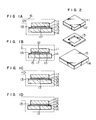
- Figs. 1A, 1B, 1C and 1D are sectional views for explaining several steps of a first embodiment of a composite structure fabricating method according to the present invention.
- Fig. 2 is an exploded, perspective view showing members which are used in the first embodiment.
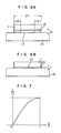
- Fig. 3 is a graph for explaining the effect of the first embodiment.
- Figs. 4A, 4B, 4C and 4D are microphotographs each showing an image which is formed by soft X-rays having passed through composite structure with a solder layer.
- Figs. 5A and 5B are sectional views for explaining that pure solder flows between a pellet and a substrate after an oxide film has been broken.
- Figs. 6A and 6B are schematic diagrams for explaining the principle of the present invention.
- Fig. 7 is a graph showing a relationship between the shape of a solder preform and the thickness of a solder layer.
- Fig. 8 is a schematic diagram showing a multi-chip cooling module which is formed by a second embodiment of a composite structure fabricating method according to the present invention.
- Fig. 9 is a perspective view showing the cooling block of Fig. 8.
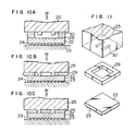
- Figs. 10A, 10B and 10C are sectional views for explaining a few steps of the second embodiment.
- Fig. 11 is an exploded, perspective view showing members which are used in the second embodiment.
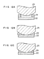
- Figs. 12A, 12B and 12C are sectional views for explaining a few steps of a modified version of the second embodiment.
- Figs. 1A to 1D are sectional views for explaining several steps which are contained in a first embodiment to form a substantially voidless solder layer
- Fig. 2 shows constituent members which are used in the present embodiment.
- reference numeral 11 designates a silicon chip including a large scale integration circuit (LSI) and having dimensions of 1 cm by 1 cm
- 12 a metallized layer formed on the rear surface of the silicon chip 11 and having a three-layer structure of Ti-Ni-Au
- 13 a looped preform which is made of Pb-Sn solder containing 40% tin by weight and has a thickness of 100 ⁇ m, and whose beltlike portion has a width of 1 mm
- 14 a heat sink made of SiC ceramics
- 15 a metallized layer formed on the surface of the heat sink 14 and having a three-layer structure of Ti-Ni-Au.
- Fig. 1A the silicon chip 11, the solder preform 13 and the heat sink 14 are piled up at the surface of a heating table (not shown) which is placed in a vacuum vessel 16, and the pressure in the vacuum vessel 16 is reduced to 133 Pa (1 Torr). At this time, the solder preform 13 is kept at a solid state. Accordingly, a small gap is inevitably formed between the solder preform 13 and each of the silicon chip 11 and the heat sink 14. Thus, the pressure in an inner region 17 surrounded by the solder preform 13 is also reduced to 133 Pa (1 Torr).
- arrows in Figs. 1A and 1C designate the direction of gas flow.
- the solder preform 13 is heated to about 220°C, to fuse the preform, thereby increasing the fluidity thereof.
- the preform 13 is kept in close contact with the metalized layers 12 and 15, or an intermetallic reaction is generated between the preform 13 and each of the metallized layers 12 and 13.
- the inner region 17 having a volume V1 is completely isolated from the outside by the preform 13, and the pressure in the inner region 17 is equal to P1 (namely, 133 Pa).
- Fig. 1B shows such a state.
- the pressure in the vacuum vessel 16 is returned to 1013 hPa (760 Torr) (namely, P2) in a state that the solder preform 13 is fused by heating. Accordingly, the solder preform 13 in a molten state is applied with an external pressure of 1013 hPa (760 Torr), and thus the volume of the inner region 17 is greatly reduced, that is, is reduced to V2.
- Fig. 1C shows such a state.
- Fig. 1D shows such a state.
- the void reduction ratio V2/V1 lay in a range from 1/100 to 1/200.
- the volume V2 was determined from that cross sectional area of a void which was obtained from the soft X-ray image of the void, and the final thickness of the solder layer 13.
- Fig. 3 is a graph showing the mean void-area of solder layers according to the present embodiment and the mean void-area of solder layers according to each of two conventional methods.
- a first conventional method that is, method 1
- the whole area of the bonding surface of one of members which are to be bonded to each other is previously coated with Pb-Sn solder containing 40% tin by weight. That is, a solder layer is previously formed.
- a second conventional method that is, method 2
- the whole area of the bonding surface of one of the members is previously coated with solder as in the method 1
- respective bonding surfaces of the members are put into contact with each other, and then four processing steps, that is, a reduction in ambient pressure, the fusion of solder, the return of ambient pressure to normal pressure, and the solidification of solder are successively made.
- the solder preform is disposed only at a periferal portion of a spatial region formed between bonding surfaces of the members.
- a mean void-area of 30 to 60% is obtained for solder layers according to each of the methods 1 and 2
- a mean void-area of around 1% is obtained for solder layers according to the method 3. That is, the present embodiment can produce a remarkable void reduction effect.
- Figs. 4A to 4D are microphotographs of images, each of which is formed by soft X-rays having passed through a solder bonded composite structure. In Figs. 4A to 4D, a white portion corresponds to a void, and a black portion corresponds to a solder layer.
- Fig. 4A shows the soft X-ray image of a composite structure according to the method 1
- Fig. 4B shows that of a composite structure according to the method 2
- Fig. 4C shows that of the structure of Fig. 1B according to the present embodiment
- Fig. 4D shows that of the structure of Fig. 1D according to the present embodiment.
- a void confined in the solder layer is made small in volume, but a void can be generated at that peripheral portion of the solder layer which is exposed to ambient atmosphere.
- the void area of the solder layer fluctuates widely, and thus it is difficult to make the void area of the solder layer less than 20%.
- an oxide film is present at the surface of the pre-coated solder layer, and it is very difficult to wet the surface of the other member well with solder.
- the inner region 17 surrounded by the solder preform (that is, an intentionally formed void) is substantially kept at a vacuum state and is isolated from ambient atmosphere by the solder preform, in an initial stage of the present embodiment. Then, pure solder is introduced into the inner region 17 in such a manner that the native oxide film on the solder preform is broken.
- pure solder is introduced into the inner region 17 in such a manner that the native oxide film on the solder preform is broken.
- the solder preform 13 is made by pouring molten solder into a mould, or is punched out from a solder sheet. In a period when the preform 13 is made in the above manner and stands in contact with air, a native oxide film 13-b shown in Fig. 5A is formed on the surface of pure solder 13-a. Accordingly, in the step of Fig. 1B, the oxide film 13-b of the solder preform 13 is kept in contact with the metallized layers 12 and 15. (In this case, a state that a part of the oxide film 13-b is broken and the pure solder 13-a flows out, can be realized by applying a load to the silicon chip 11, or other methods. In a conventional method, a mechanical vibration is applied to the silicon chip 11, to produce such a state, thereby improving the wettability for solder.
- Fig. 5B corresponds to Fig. 1C, and shows a state that the oxide film 13-b has been broken and the pure solder 13-a has flowed into the inner region 17. It was confirmed by the Auger electron spectroscopy that the oxide film 13 was present only at a peripheral portion of each metallized layer.
- each of the metallized layers 12 and 15 is uniformly wetted with solder.
- a reduction in bonding strength due to a fact that a bonding surface is not wetted uniformly with solder never occurs, though the above reduction is generated in the B-method disclosed in the above-referred Japanese patent application JP-A-61-125,025.
- the void of the solder layer is reduced in a surprising degree, and moreover a solder bonded composite structure can be readily formed, in which the bonding surfaces of two members are wetted well with solder. Accordingly, when a semiconductor chip is bonded to a heat sink by the present embodiment, a semiconductor device formed has a remarkable heat-radiating ability, and hence will be excellent in thermal performance and reliability.
- the thickness of a solder layer according to the present embodiment can be readly controlled.
- Figs. 6A and 6B are schematic diagrams for explaining the principle of the present invention, and show the steps of Figs. 1B and 1D, respectively.
- Figs. 6A and 6B when the thickness of the solder preform, the thickness of the bonding solder layer, the width of beltlike portions of the solder preform, and the length of one side of the solder preform are expressed by t0, t , d , and 2r, respectively, we can obtain the following formula: where 0 ⁇ d r ⁇ 1
- Fig. 7 is a graph which shows a relation between d/r and t/t0 given by the formula (1).
- the thickness t0, half-length r and width d with respect to the solder preform 13 are made equal to 100 ⁇ m, 5 mm and 1 mm, respectively, by way of example. Accordingly, the thickness t of the bonding solder layer calculated from the formula (1) is nearly equal to 36 ⁇ m. This value corresponds to the measured values of the thickness t for a multiplicity of samples lying in a range from 30 to 40 ⁇ m. In other words, since the bonding solder layer has a void of 1% or less, the thickness of the bonding solder layer can be accurately controlled on the basis of the formula (1). Thus, according to the present embodiment, the thickness of the bonding solder layer can be accurately determined so that a composite structure is optimum in thermal and mechanical properties.
- the following table shows the change of state of the hermetically sealed region 17 in steps (b), (c) and (d) which are shown in Figs. 1B, 1C and 1D, respectively.
- P1, P2, T1, T2 and T3 are made equal to 133 Pa, 1013 hPa, 220°C (temperature of heating table), 183°C (melting point of solder) and 25°C (normal temperature), respectively, by way of example. It is to be noted that the step (d) is followed by the step (d ⁇ ), in which the solidified solder is cooled to normal temperature.
- the final volume V2 of the void confined in the bonding solder layer is equal to which is nearly equal to 1.2 ⁇ 10 ⁇ 3 V1.
- the void volume of the bonding solder layer in the final stage can be determined from the initial volume V1 of the inner region 17.
- the EMBODIMENT I a single semiconductor pellet is bonded to a heat sink by solder.
- the EMBODIMENT I deals with a case where the semiconductor pellet is relatively small in weight and the bonding surfaces of the pellet and the heat sink are flat.
- Fig. 8 shows a case where each of a plurality of semiconductor chips 22 is mounted on a corresponding one of cooling blocks 25 through a solder layer 29 to form a multi-chip cooling module. The method described in the EMBODIMENT I is not applicable to such a case.
- Fig. 8 shows a multi-chip cooling module similar to a module which is disclosed in a Japanese patent application JP-A-60-94,749 entitled "integration circuit chip cooling device".
- silicon chips 22 each having a large scale integration circuit is enclosed in and cooled by a cooling module 21. Further, the silicon chips 22 are connected to a circuit board 24 through solder bumps 23.
- a fin (not shown) is provided in a cooling block 25, to be connected to a coolant path 27 through bellows 26. That is, when cooling water is caused to flow from an inlet 28-a to an outlet 28-b, heat is removed from the cooling block.
- the silicon chip 22 is bonded to the cooling block 25 through a solder layer 29.
- Fig. 9 is a perspective view showing a cooling block 25 which is mounted with a silicon chip 22.
- cooling module As can be readily seen from the structure of cooling module shown in Fig. 8, owing to variations in length of the flexible bellows 26, a warp in the circuit board 24, variations in height of the solder bumps 23, and others, the distance between the cooling block 25 and the silicon chip 22 fluctuates. Accordingly, when the silicon chip 22 is bonded to the cooling block 25 by solder, it is required to apply an appropriate vertical load to the cooling block 25 so that molten solder is kept in chose contact with the chip 22 and the block 25.
- Figs. 10A to 10C are sectional views showing a few steps of the present embodiment which can solve the above problem and can form a voidless solder layer
- Fig. 11 is an exploded perspective view showing members which are used in the present embodiment.
- protrusions 30 are formed on the bonding surface of the cooling block 25, to prevent fused solder from flowing out.
- a spacer having an appropriate thickness may be attached to the bonding surface.
- Figs. 10A to 10C show steps corresponding to those of Figs. 1A to 1C. As shown in Fig.
- Figs. 12A to 12C are sectional views showing steps of a modified version of the present embodiment.
- a spherical bonding surface is used as an unflat surface.
- Figs. 12A to 12C show steps corresponding to those of Figs. 1A to 1C. As shown in Fig. 12C, even when a spherical bonding surface is used, a homogeneous solder layer is formed, and a composite structure is accurately constructed.
- the thickness of the solder preform serving as an intermediate member can be univocally and readily determined.
- the present invention is applicable to a case where a bonding surface includes an unflat portion.
- a bonding surface having the protursions 30 has been used, to solve the problem caused by a vertical load.
- the formation of a voidless solder layer on an unflat surface according to the present invention is applicable to and can exhibit a remarkable effect in various fields.
- the solder preform is used as a fusible intermediate member.
- the effect of the present invention can be obtained independently of the kind and size of the fusible member, the kind and size of main members to be bonded to each other, and the set state of the fusible member, provided that the fusible member is disposed on a peripheral portion of the bonding surface of one main member.
- the effect of the present invention can be obtained only by making the adhesive agent flowable at a time ambient pressure is increased.
- fusible materials other than solder for example, an organic resin is used, the present invention can produce the same effect as mentioned above.
- the ambient pressure P is first reduced to vacuum (P1), and then increased to normal pressure (P2).
- the void reduction which is the gist of the present invention is proportional to the pressure ratio P1/P2, and the initial pressure P1 is so set as to be lower than the final pressure P2. That is, it is not required to set the pressure P1 as mentioned in the EMBODIMENTS, but the pressure P1 is determined while taking into consideration the simplicity of operation. For example, when the pressure P1 is made equal to normal pressure (1013 hPa), the pressure P2 is set to a pressure higher than 1013 hPa. In this case, also, the present invention can produce the same effect as in the EMBODIMENTS.
- a solder layer for bonding is controllably formed which has very small in volume and is kept in close contact with the bonding surfaces of main members. Further, pure solder flows on the bonding surfaces in a state that the surface oxide film of solder has been broken, and hence fluxless soldering can be made.
- a solder layer formed between the chip and the heat sink will be small in thermal resistance and large in bonding strength. Thus, the performance and reliability of the composite structure are greatly improved. Further, according to the present invention, even in a case where it is required from the practical point of view to apply a load to one of main members, a solder layer is prevented from flowing out or flying apart from the bonding surfaces of the main members.
Landscapes
- Die Bonding (AREA)
- Cooling Or The Like Of Semiconductors Or Solid State Devices (AREA)
Claims (9)
- Verfahren zum Herstellen einer Verbundstruktur, die derart ausgebildet ist, daß ein Zwischenelement (13; 29) zwischen einem ersten und einem zweiten Element (11, 14; 22, 25) sandwichartig angeordnet ist, wobei das Verfahren folgende Schritte umfaßt:
Anordnen des Zwischenelements (13; 29) entlang dem Umfang eines zwischen einander zugewandten Oberflächen des ersten und des zweiten Elements (11, 14; 22, 25) gebildeten räumlichen Bereichs, so daß dieser von dem Zwischenelement (13; 29) umschlossen ist;
Erhöhen der Fluidität des Zwischenelements (13; 29) in einer Atmosphäre mit einem vorbestimmten Druck; und
Erhöhen des Drucks dieser Atmosphäre, um ein Fließen des Zwischenelements (13; 29) in den räumlicher Bereich zu bewirken. - Verfahren zum Herstellen einer Verbundstruktur nach Anspruch 1, wobei die Dicke des Zwischenelements (29) größer als die Dicke eines vorher zwischen dem ersten und dem zweiten Element (22, 25) vorgesehenen Abstandsstücks (30) ist.
- Verfahren zum Herstellen einer Verbundstruktur, die derart ausgebildet ist, daß ein Zwischenelement (13; 29) zwischen einem ersten und einem zweiten Element (11, 14; 22, 25) sandwichartig angeordnet ist, wobei das Verfahren folgende Schritte aufweist:
Anordnen des Zwischenelements (13; 29) entlang dem Umfang eines zwischen einander zugewandten Oberflächen des ersten und des zweiten Elements (11, 14; 22, 25) gebildeten räumlichen Bereichs, so daß dieser von dem Zwischenelement (13; 29) umschlossen ist;
Verringern des Drucks einer Atmosphäre, in der das erste und das zweite Element sowie das Zwischenelement angeordnet sind;
Erhöhen der Fluidität des Zwischenelements (13; 29) in dieser Atmosphäre mit verringertem Druck durch Erwärmen des Zwischenelements (13; 29); und
Erhöhen des Drucks dieser Atmosphäre. - Verfahren zum Herstellen einer Verbundstruktur nach Anspruch 3, wobei der Druck der genannten Atmosphäre in dem Druckverringerungsschritt auf weniger Atmosphärendruck verringert und in dem Druckerhöhungsschritt wieder auf Atmosphärendruck gebracht wird.
- Verfahren zum Herstellen einer Verbundstruktur nach Anspruch 3, wobei das Zwischenelement (13; 29) ein Vorformling mit einer vorbestimmten Form ist.
- Verfahren zum Herstellen einer Verbundstruktur nach Anspruch 3, wobei das Zwischenelement (13; 29) aus Lot hergestellt wird.
- Verfahren zum Herstellen einer Verbundstruktur nach Anspruch 3, wobei das Zwischenelement (13; 29) aus Pb-Sn-Lot hergestellt wird.
- Verfahren zum Herstellen einer Verbundstruktur nach Anspruch 3, wobei auf denjenigen Oberflächen des ersten und des zweiten Elements (12, 15), die mit dem Zwischenelement (13) zu verbinden sind, Metallisierungsschichten (12, 15) gebildet werden.
- Verfahren zum Herstellen einer Verbundstruktur nach Anspruch 4, wobei der Druck der genannten Atmosphäre in dem Druckverringerungsschritt auf weniger als 1/100 des Atmosphärendrucks verringert wird.
Applications Claiming Priority (4)
| Application Number | Priority Date | Filing Date | Title |
|---|---|---|---|
| JP24525286 | 1986-10-17 | ||
| JP245252/86 | 1986-10-17 | ||
| JP56528/87 | 1987-03-13 | ||
| JP62056528A JP2510557B2 (ja) | 1986-10-17 | 1987-03-13 | 複合構造体の製造方法 |
Publications (3)
| Publication Number | Publication Date |
|---|---|
| EP0264122A2 EP0264122A2 (de) | 1988-04-20 |
| EP0264122A3 EP0264122A3 (en) | 1989-06-07 |
| EP0264122B1 true EP0264122B1 (de) | 1992-03-18 |
Family
ID=26397487
Family Applications (1)
| Application Number | Title | Priority Date | Filing Date |
|---|---|---|---|
| EP87115028A Expired - Lifetime EP0264122B1 (de) | 1986-10-17 | 1987-10-14 | Verfahren zum Herstellen einer gemischten Struktur für Halbleiteranordnung |
Country Status (3)
| Country | Link |
|---|---|
| US (1) | US4819857A (de) |
| EP (1) | EP0264122B1 (de) |
| DE (1) | DE3777522D1 (de) |
Families Citing this family (21)
| Publication number | Priority date | Publication date | Assignee | Title |
|---|---|---|---|---|
| US4927069A (en) * | 1988-07-15 | 1990-05-22 | Sanken Electric Co., Ltd. | Soldering method capable of providing a joint of reduced thermal resistance |
| DE3914333A1 (de) * | 1989-04-29 | 1990-10-31 | Hoechst Ceram Tec Ag | Pumpenkolben fuer axialkolbenpumpen |
| JPH0357230A (ja) * | 1989-07-25 | 1991-03-12 | Mitsubishi Electric Corp | 半導体基板と支持板とのロウ付け方法 |
| EP0460286A3 (en) * | 1990-06-06 | 1992-02-26 | Siemens Aktiengesellschaft | Method and arrangement for bonding a semiconductor component to a substrate or for finishing a semiconductor/substrate connection by contactless pressing |
| US5906310A (en) * | 1994-11-10 | 1999-05-25 | Vlt Corporation | Packaging electrical circuits |
| JP2732823B2 (ja) * | 1995-02-02 | 1998-03-30 | ヴィエルティー コーポレーション | はんだ付け方法 |
| CA2156941A1 (en) * | 1995-08-21 | 1997-02-22 | Jonathan H. Orchard-Webb | Method of making electrical connections to integrated circuit |
| GB2316225A (en) | 1996-08-06 | 1998-02-18 | Northern Telecom Ltd | Semiconductor photodetector packaging |
| US6070321A (en) * | 1997-07-09 | 2000-06-06 | International Business Machines Corporation | Solder disc connection |
| US6095400A (en) * | 1997-12-04 | 2000-08-01 | Ford Global Technologies, Inc. | Reinforced solder preform |
| US6316737B1 (en) | 1999-09-09 | 2001-11-13 | Vlt Corporation | Making a connection between a component and a circuit board |
| JP3946393B2 (ja) * | 1999-10-19 | 2007-07-18 | 株式会社東芝 | 階層構造をもつ並列計算機 |
| US6985341B2 (en) | 2001-04-24 | 2006-01-10 | Vlt, Inc. | Components having actively controlled circuit elements |
| CN1255563C (zh) * | 2001-05-24 | 2006-05-10 | 弗莱氏金属公司 | 热界面材料和受热器构型 |
| CA2547358C (en) * | 2001-05-24 | 2013-08-06 | Fry's Metals, Inc. | Thermal interface material and solder preforms |
| US6848610B2 (en) * | 2003-03-25 | 2005-02-01 | Intel Corporation | Approaches for fluxless soldering |
| WO2006137823A2 (en) * | 2004-06-17 | 2006-12-28 | The Regents Of The University Of California | Designs and fabrication of structural armor |
| US7723830B2 (en) * | 2006-01-06 | 2010-05-25 | International Rectifier Corporation | Substrate and method for mounting silicon device |
| DE102008001221A1 (de) * | 2007-04-24 | 2008-10-30 | Ceramtec Ag | Bauteil mit einem keramischen Körper mit metallisierter Oberfläche |
| US8076773B2 (en) * | 2007-12-26 | 2011-12-13 | The Bergquist Company | Thermal interface with non-tacky surface |
| TWI896542B (zh) | 2019-07-23 | 2025-09-11 | 德商漢高股份有限及兩合公司 | 高熱通量多元件總成之熱管理 |
Citations (1)
| Publication number | Priority date | Publication date | Assignee | Title |
|---|---|---|---|---|
| JPS61125025A (ja) * | 1984-11-22 | 1986-06-12 | Hitachi Ltd | 半導体装置の製造方法 |
Family Cites Families (12)
| Publication number | Priority date | Publication date | Assignee | Title |
|---|---|---|---|---|
| US3648357A (en) * | 1969-07-31 | 1972-03-14 | Gen Dynamics Corp | Method for sealing microelectronic device packages |
| DE2032939B2 (de) * | 1970-07-03 | 1975-05-07 | Robert Bosch Gmbh, 7000 Stuttgart | Verfahren zum Auflöten eines Halbleiterkörpers auf einen Träger |
| US3711939A (en) * | 1970-11-10 | 1973-01-23 | M Stoll | Method and apparatus for sealing |
| JPS5614069A (en) * | 1979-07-16 | 1981-02-10 | Nec Corp | Soldering method and soldering material |
| DE2939666C2 (de) * | 1979-09-29 | 1982-07-15 | Robert Bosch Gmbh, 7000 Stuttgart | Verfahren zur lunkerfreien Verlötung eines metallisierten Halbleiterplättchens mit einem Träger |
| US4645116A (en) * | 1982-10-08 | 1987-02-24 | At&T Bell Laboratories | Fluxless bonding of microelectronic chips |
| JPH0673364B2 (ja) * | 1983-10-28 | 1994-09-14 | 株式会社日立製作所 | 集積回路チップ冷却装置 |
| US4574470A (en) * | 1984-03-19 | 1986-03-11 | Trilogy Computer Development Partners, Ltd. | Semiconductor chip mounting system |
| JPS60214536A (ja) * | 1984-04-09 | 1985-10-26 | Fujitsu Ltd | 半導体装置の製造方法 |
| DE3442537A1 (de) * | 1984-11-22 | 1986-05-22 | BBC Aktiengesellschaft Brown, Boveri & Cie., Baden, Aargau | Verfahren zum blasenfreien verbinden eines grossflaechigen halbleiter-bauelements mit einem als substrat dienenden bauteil mittels loeten |
| US4604644A (en) * | 1985-01-28 | 1986-08-05 | International Business Machines Corporation | Solder interconnection structure for joining semiconductor devices to substrates that have improved fatigue life, and process for making |
| US4709849A (en) * | 1985-11-27 | 1987-12-01 | Fry Metals, Inc. | Solder preform and methods employing the same |
-
1987
- 1987-10-14 EP EP87115028A patent/EP0264122B1/de not_active Expired - Lifetime
- 1987-10-14 DE DE8787115028T patent/DE3777522D1/de not_active Expired - Lifetime
- 1987-10-19 US US07/109,449 patent/US4819857A/en not_active Expired - Lifetime
Patent Citations (1)
| Publication number | Priority date | Publication date | Assignee | Title |
|---|---|---|---|---|
| JPS61125025A (ja) * | 1984-11-22 | 1986-06-12 | Hitachi Ltd | 半導体装置の製造方法 |
Also Published As
| Publication number | Publication date |
|---|---|
| EP0264122A2 (de) | 1988-04-20 |
| EP0264122A3 (en) | 1989-06-07 |
| DE3777522D1 (de) | 1992-04-23 |
| US4819857A (en) | 1989-04-11 |
Similar Documents
| Publication | Publication Date | Title |
|---|---|---|
| EP0264122B1 (de) | Verfahren zum Herstellen einer gemischten Struktur für Halbleiteranordnung | |
| TW392318B (en) | Semiconductor device, and manufacturing method of the same | |
| US5387815A (en) | Semiconductor chip module | |
| US6794223B2 (en) | Structure and process for reducing die corner and edge stresses in microelectronic packages | |
| US4862322A (en) | Double electronic device structure having beam leads solderlessly bonded between contact locations on each device and projecting outwardly from therebetween | |
| US6130112A (en) | Semiconductor device | |
| KR940001283B1 (ko) | 세라믹팩형 반도체 장치 및 그의 조립방법 | |
| US6656770B2 (en) | Thermal enhancement approach using solder compositions in the liquid state | |
| US7863098B2 (en) | Flip chip package with advanced electrical and thermal properties for high current designs | |
| US5982038A (en) | Cast metal seal for semiconductor substrates | |
| EP0237741A2 (de) | Wärmeleitende Anordnung | |
| KR930009314B1 (ko) | 열전도성 복합재 | |
| JPS61201452A (ja) | 集積回路チツプ冷却装置 | |
| US7672132B2 (en) | Electronic packaging apparatus and method | |
| US20020105073A1 (en) | Low cost and compliant microelectronic packages for high i/o and fine pitch | |
| US20020191377A1 (en) | Material of heat-dissipating plate on which semiconductor is mounted, method for fabricating the same, and ceramic package produced by using the same | |
| EP2232550B1 (de) | Thermische verbindung eines halbleiterbauelements | |
| US5046656A (en) | Vacuum die attach for integrated circuits | |
| EP0392109A2 (de) | Wärmeleitendes zusammengesetztes Material | |
| JP2003017625A (ja) | インターポーザおよび半導体パッケージ | |
| US4974769A (en) | Method of joining composite structures | |
| EP1553627A1 (de) | Material für eine wärmeabführende Platte, auf der ein Halbleiter montiert ist, und hieraus produziertes keramisches Gehäuse | |
| JP2510557B2 (ja) | 複合構造体の製造方法 | |
| JPH11135691A (ja) | 電子回路装置 | |
| JP3493833B2 (ja) | 半導体素子搭載用プラスチックパッケージおよびその製造方法 |
Legal Events
| Date | Code | Title | Description |
|---|---|---|---|
| PUAI | Public reference made under article 153(3) epc to a published international application that has entered the european phase |
Free format text: ORIGINAL CODE: 0009012 |
|
| AK | Designated contracting states |
Kind code of ref document: A2 Designated state(s): DE FR GB |
|
| PUAL | Search report despatched |
Free format text: ORIGINAL CODE: 0009013 |
|
| AK | Designated contracting states |
Kind code of ref document: A3 Designated state(s): DE FR GB |
|
| 17P | Request for examination filed |
Effective date: 19890612 |
|
| 17Q | First examination report despatched |
Effective date: 19910527 |
|
| GRAA | (expected) grant |
Free format text: ORIGINAL CODE: 0009210 |
|
| AK | Designated contracting states |
Kind code of ref document: B1 Designated state(s): DE FR GB |
|
| REF | Corresponds to: |
Ref document number: 3777522 Country of ref document: DE Date of ref document: 19920423 |
|
| ET | Fr: translation filed | ||
| PLBE | No opposition filed within time limit |
Free format text: ORIGINAL CODE: 0009261 |
|
| STAA | Information on the status of an ep patent application or granted ep patent |
Free format text: STATUS: NO OPPOSITION FILED WITHIN TIME LIMIT |
|
| 26N | No opposition filed | ||
| PGFP | Annual fee paid to national office [announced via postgrant information from national office to epo] |
Ref country code: FR Payment date: 20010830 Year of fee payment: 15 |
|
| PGFP | Annual fee paid to national office [announced via postgrant information from national office to epo] |
Ref country code: GB Payment date: 20011008 Year of fee payment: 15 |
|
| PGFP | Annual fee paid to national office [announced via postgrant information from national office to epo] |
Ref country code: DE Payment date: 20011228 Year of fee payment: 15 |
|
| REG | Reference to a national code |
Ref country code: GB Ref legal event code: IF02 |
|
| PG25 | Lapsed in a contracting state [announced via postgrant information from national office to epo] |
Ref country code: GB Free format text: LAPSE BECAUSE OF NON-PAYMENT OF DUE FEES Effective date: 20021014 |
|
| PG25 | Lapsed in a contracting state [announced via postgrant information from national office to epo] |
Ref country code: DE Free format text: LAPSE BECAUSE OF NON-PAYMENT OF DUE FEES Effective date: 20030501 |
|
| GBPC | Gb: european patent ceased through non-payment of renewal fee |
Effective date: 20021014 |
|
| PG25 | Lapsed in a contracting state [announced via postgrant information from national office to epo] |
Ref country code: FR Free format text: LAPSE BECAUSE OF NON-PAYMENT OF DUE FEES Effective date: 20030630 |
|
| REG | Reference to a national code |
Ref country code: FR Ref legal event code: ST |