EP0264913A2 - Plasmabearbeitungsgerät - Google Patents
Plasmabearbeitungsgerät Download PDFInfo
- Publication number
- EP0264913A2 EP0264913A2 EP87115349A EP87115349A EP0264913A2 EP 0264913 A2 EP0264913 A2 EP 0264913A2 EP 87115349 A EP87115349 A EP 87115349A EP 87115349 A EP87115349 A EP 87115349A EP 0264913 A2 EP0264913 A2 EP 0264913A2
- Authority
- EP
- European Patent Office
- Prior art keywords
- plasma
- slit
- microwaves
- processing apparatus
- cavity resonator
- Prior art date
- Legal status (The legal status is an assumption and is not a legal conclusion. Google has not performed a legal analysis and makes no representation as to the accuracy of the status listed.)
- Granted
Links
Images


Classifications
-
- H—ELECTRICITY
- H01—ELECTRIC ELEMENTS
- H01J—ELECTRIC DISCHARGE TUBES OR DISCHARGE LAMPS
- H01J37/00—Discharge tubes with provision for introducing objects or material to be exposed to the discharge, e.g. for the purpose of examination or processing thereof
- H01J37/32—Gas-filled discharge tubes
- H01J37/32009—Arrangements for generation of plasma specially adapted for examination or treatment of objects, e.g. plasma sources
- H01J37/32192—Microwave generated discharge
- H01J37/32211—Means for coupling power to the plasma
- H01J37/32238—Windows
-
- C—CHEMISTRY; METALLURGY
- C23—COATING METALLIC MATERIAL; COATING MATERIAL WITH METALLIC MATERIAL; CHEMICAL SURFACE TREATMENT; DIFFUSION TREATMENT OF METALLIC MATERIAL; COATING BY VACUUM EVAPORATION, BY SPUTTERING, BY ION IMPLANTATION OR BY CHEMICAL VAPOUR DEPOSITION, IN GENERAL; INHIBITING CORROSION OF METALLIC MATERIAL OR INCRUSTATION IN GENERAL
- C23C—COATING METALLIC MATERIAL; COATING MATERIAL WITH METALLIC MATERIAL; SURFACE TREATMENT OF METALLIC MATERIAL BY DIFFUSION INTO THE SURFACE, BY CHEMICAL CONVERSION OR SUBSTITUTION; COATING BY VACUUM EVAPORATION, BY SPUTTERING, BY ION IMPLANTATION OR BY CHEMICAL VAPOUR DEPOSITION, IN GENERAL
- C23C16/00—Chemical coating by decomposition of gaseous compounds, without leaving reaction products of surface material in the coating, i.e. chemical vapour deposition [CVD] processes
- C23C16/44—Chemical coating by decomposition of gaseous compounds, without leaving reaction products of surface material in the coating, i.e. chemical vapour deposition [CVD] processes characterised by the method of coating
- C23C16/50—Chemical coating by decomposition of gaseous compounds, without leaving reaction products of surface material in the coating, i.e. chemical vapour deposition [CVD] processes characterised by the method of coating using electric discharges
- C23C16/517—Chemical coating by decomposition of gaseous compounds, without leaving reaction products of surface material in the coating, i.e. chemical vapour deposition [CVD] processes characterised by the method of coating using electric discharges using a combination of discharges covered by two or more of groups C23C16/503 - C23C16/515
-
- H—ELECTRICITY
- H01—ELECTRIC ELEMENTS
- H01J—ELECTRIC DISCHARGE TUBES OR DISCHARGE LAMPS
- H01J37/00—Discharge tubes with provision for introducing objects or material to be exposed to the discharge, e.g. for the purpose of examination or processing thereof
- H01J37/32—Gas-filled discharge tubes
- H01J37/32009—Arrangements for generation of plasma specially adapted for examination or treatment of objects, e.g. plasma sources
- H01J37/32192—Microwave generated discharge
- H01J37/32211—Means for coupling power to the plasma
- H01J37/32247—Resonators
Definitions
- This invention relates to fabrication of semiconductor devices using low temperature plasma, and more particularly to a plasma processing apparatus suited for carrying out the respective techniques of CVD, etching, sputtering, ashing, etc. at high speed.
- Devices using low-temperature plasma roughly includes two categories one consisting of applying a high frequency voltage at about 10 KHz to 30 MHz to one of parallel plate electrodes in vacuum to create plasma (see "HANDOTAI KENKYU" No. 18, pages 121 - 137, 145 - 169); and the other of introducing a microwave at 2.45 GHz into a vacuum chamber to create plasma.
- the device belonging to the former category has been mainly used.
- the miniaturization of semiconductor devices has caused the problem that the bombardment of ions which is generated in plasma-processing thereof disadvantageously influences the device performance. It has been also required to increase the processing speed in order to improve the processing capability.
- the energy of ions plays an important role in dry etching using plasma and plasma CVD.
- dry etching if the ion energy is too high, the underlying film will be cut or the crystal structure will be badly influenced, thus deteriorating the device performance.
- the ion energy is too low, the polymer formed on the etched face will not be sufficiently removed, thus reducing the etching speed; or inversely a passivation film of the polymer will not be formed but the side of the pattern will be etched, thus reducing the dimension accuracy of the pattern.
- the magnitude of ion energy influences the quality of the formed film in such a way that low ion energy leads to coarse film composition while high ion energy leads to dense film composition.
- Examples of such a plasma processing are the systems of producing plasma using microwaves such as disclosed in JP-A-56-13480 (U.S.P. No. 4,492,620), and JP-A-56-96841.
- the plasma generated through the microwaves includes the electrons directly supplied with energy from the microwaves so that the voltage across the sheath formed between the plasma and the substrate does not almost vary.
- the plasma generated through the microwaves includes the electrons directly supplied with energy from the microwaves so that the voltage across the sheath formed between the plasma and the substrate does not almost vary.
- the plasma is produced in a cavity resonator so that when the plasma is produced, the wavelength of the microwaves is changed according to the plasma density.
- the resonance condition is not satisfied and accordingly the plasma will be unstable. More specifically, since the resonance condition is satisfied before the plasma is produced, the electric field strength of the microwaves becomes greater, thus eventually producing the plasma.
- the resonance condition will not be satisfied, thereby decreasing the electric field strength. Then, the electrons will be supplied with lower energy and so the plasma density will be decreased. Once the plasma density is decreased, the resonance condition will be satisfied again and the plasma density will be higher. Due to such a phenomenon, it is difficult to produce stabilized plasma using the cavity resonator.
- the electrode for applying a high frequency voltage is arranged in the cavity resonator in order to control the energy of the ions incident to the substrate from the plasmas, the reflection of the microwave or the like will occur so that the plasma formed will furtheron be unstable.
- the object of this invention is to provide a plasma processing apparatus which is capable of producing stabilized and high density plasma and making uniform the energy of ions incident to a substrate over the entire substrate.
- a plasma processing apparatus comprising a microwave generation source, a waveguide for supplying the microwaves from the microwave generation source, a cavity resonator at an atmospheric pressure connected with the end of the waveguide to resonate the microwaves, a plasma production chamber, and a slit provided for relatively uniformly emitting the resonated microwaves into the plasma production chamber.
- the microwaves when the microwaves propagate in the cavity resonator, the microwaves are resonated by the wall in the resonator and the like and also the current corresponding to the electromagnetic field generated flows in the interior surface.
- the slit is provided at the boundary between the cavity resonator and the plasma production chamber so as to traverse the current, charges are accumulated at both ends of the slit. Since the amount of the charges accumulated is varied along with the propagation of the microwaves, the electric field at both ends of the slit is also varied. Thus, the microwaves are uniformly emitted from the cavity resonator into the plasma production chamber.
- the microwaves the amplitude of which has been increased through the resonance in the cavity resonator is emitted into the plasma production chamber through the slit the area of which is about one third times or one 10th times the sectional area of the resonator.
- the electrode structure according to this invention doesn't have any restriction relative to the cavity resonator. Moreover, since the plasma is not produced in the cavity resonator, the resonance state therein remains unchanged, and so the stabilized plasma can be produced. Further, the cavity resonator connected to ground can be used as an electrode opposite to and in parallel to the electrode on which the substrate is placed, as in the system of parallel plate electrodes so that the effect of ion energy can be made uniform over the entire substrate.
- Another gist of this invention is that a slit plate integral to the cavity resonator and having plural slit-like openings extended towards the plasma production chamber is provided and gas flow paths from a gas supply source to the plasma production chamber are provided among the plural openings.
- the gas flow paths are formed among the slit-like openings of the slit plate so as to open towards the plasma production chamber so that gas can be supplied shower-like into the plasma production chamber without obstructing the path for introducing the microwaves.
- high density plasma can be uniformly provided to the entire substrate.
- this invention is also characterized in that the slit is formed by a plating technique, that a high frequency power supply is connected between a conductive slit plate with slits and the electrode on which the substrate is placed, and that the application of the high frequency voltage is switched between the slit plate and the electrode.
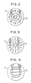
- Fig. 1 is a circular cavity resonator in E01 mode to which microwaves are supplied from a magnetron 3 through a waveguide 2.
- the waveguide 2 is eccentrically attached to one side of the circular cavity resonator 1 so as to provide a desired coupling with the E01 mode.
- On the other side of the circular cavity resonator 1 are attached a ceramic plate 4 and a slit plate 5 in this order.
- the slit plate 5 is connected with a plasma production chamber 6.
- the plasma production chamber 6 is separated from a circular cavity resonator 1 by a plate made of microwave-transmitting materials such as ceramics or quartz.
- the circular cavity resonator 1 is at atmospheric pressure in its interior in which microwaves are reflected at the inner wall so as to be resonated. Therefore, the microwaves supplied through the waveguide 2 are resonated in the circular cavity resonator 1 so that they are increased in their amplitude and so energy.
- the planar structure of the slit plate 5 is shown by 5b in Fig. 2.
- the slit part 5b includes ring-shape slit openings (referred to as simply slits) in the direction perpendicular to the electric field in E01 mode.
- the resonance in the E01 mode occurs in the electric field distribution as shown in Fig. 10.
- the surface current as indicated by broken lines flows on the interior surface of the cavity resonator 1.
- the surface current on the bottom surface of the cavity resonator 1 flows from its center towards its periphery as shown in Fig. 2 that is indicated by broken lines.
- the slit plate 5 is located at the position corresponding to this bottom surface and so the slits 5c are provided in the direction perpendicular to the surface current.
- the charges due to the surface current are accumulated at both ends of each of the slits 5 so that the electric field is generated in the slit part 5.
- This electric field is varied with the frequency of 2.45 GHz so that the microwaves are emitted from the slits 5c.
- the length of the slits 5c is set at 60 mm, which corresponds to 1/2 of the wavelength of the microwave (2.45 GHz), or more to satisfactorily emit the microwaves.
- the width of the slits 5c ranges preferably from 5 mm to 15 mm although it varies in accordance with the kind of processing gas.
- many slits 5c are provided so as to occupy about one third to one 10th of the entire area of the slit plate 5.
- an electrode 7 on which the substrate to be processed is placed, a gas supply tube 9 and a gas exhaust tube 10.
- the electrode is fixed to the plasma production chamber 6 by means of an insulator 8 and is connected with a high frequency power supply 11.
- the gas supply tube 9 is adapted to supply a predetermined amount of plasma processing gas from a gas source (not shown).
- the gas exhaust tube 10, which is connected with a vacuum evacuation pump, is adapted to control the pressure in the plasma production chamber in the range of 1 to 10 ⁇ 3 Torr.
- the magnetron 3 is operated to oscillate the microwaves which are supplied to the circular cavity resonator 1 through the waveguide 2.
- the energy of the microwaves with the amplitude increased in the cavity resonator 1 is emitted into the plasma production chamber 6 through the slits 5c. Since the amplitude of the microwaves emitted into the plasma production chamber 6 has been increased in the cavity resonator 1, plasma is produced in the plasma production chamber 6 even if the plasma production chamber 6 has not a cavity resonator structure.
- etching gas is supplied from the gas supply tube 9 into the plasma production chamber 6.
- the plasma production chamber 6 evacuated to a prescribed pressure from the gas exhaust tube 10, the plasma due to the microwaves is produced between the slit plate 5 and the electrode 7. (Since the microwaves directly act on the electrons in the plasma, the potential difference between the plasma and the electrode 7 is in the level of 20 to 30V.)
- a high frequency voltage is applied to the electrode 7 from the high frequency power supply 11.
- the electrode 7 and the slit plate 5 connected to ground are arranged in parallel to each other, a high frequency current uniformly flows between the electrode 7 and the slit plate 5 connected to ground.
- the electric field occurring between the electrode 7 and the plasma becomes unifrom.
- the ions of etching gas are controlled so as to be incident to the wafer 12 with the uniform energy over the entire wafer surface.
- the ions in the etching gas and/or the radicals of the etching gas excited in the plasma act on the film to be processed on the wafer 12. By this way, the etching proceeds. Since the energy of the incident ions during the etching is uniform, the etching can be carried out uniformly over the entire wafer.
- the resonance mode in the circular cavity resonator 1 was the E01 mode
- any other suitable mode can be used.
- the emission efficiency is higher when the slits are in the direction pependicular to the current flowing in the cavity resonator surface.
- the slit plate preferably has the structure as shown in Fig. 3 in the case of H01 mode and the structure as shown in Fig. 4, in the case of H11 mode (Refer to "Microwave Technique" by H. Abe, Tokyo Univ. pp. 71 - 74, 105 - 108, 143 - 145.)
- the effect of ion energy indispensable to the plasma processing can be made uniform and also stabilized plasma can be produced.
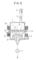
- the microwaves are only emitted into the plasma production chamber. Therefore, when the density of the produced plasma exceeds 1011cm ⁇ 3, the microwaves are reflected and the plasma density cannot be further enhanced. Thus, if the plasma density is greater than 1011cm ⁇ 3, a magnetic field 15 which is in parallel to the emitting direction of the microwaves is provided by coils 13 and 14 as shown in Fig. 5.
- the amplitude of the microwaves is increased in the cavity resonator 1, the state of electron cyclotron resonance is not required, but the magnetic field strength in accordance with the required plasma density can be selected. Moreover, since the amplitude of the microwaves can be made greater than the prior art resonance system, stabilized plasma discharge can be produced in the region evacuated to a higher degree.
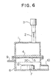
- a mesh plate 20 is located in the interior of the plasma production (processing) chamber 6 and a wafer 12 is placed on a table 7 which is also provided in the chamber 6.
- Oxygen gas is supplied from the gas supply tube 9.
- the magnetron 3 is operated to supply microwaves thereby to produce plasma between the slit plate 5 and the mesh plate 20.
- the mesh plate 20 Since the mesh plate 20 is dimensioned so as not to transmit the microwaves, the plasma is confined between the mesh plate 20 and the slit plate 5.
- the oxygen gas which has been placed in the radical state due to the plasm is supplied onto the wafer 12 through the mesh plate 20.
- the oxygen radicals ashing-process the resist film on the wafer.
- a processing chamber 33 made of ceramics or quartz is adapted to control the pressure therein in the range of 10 ⁇ 4 Torr to 10 ⁇ 2 Torr by means of a gas supply tube and a gas exhaust tube.
- a target 34 and a wafer table 36 are placed in the processing chamber 33.
- the target 34 is connected with a high frequency power supply 35, and the wafer table 36 is connected to ground.
- a shield chamber 40 and a square-ring shape resonator 31 are provided on the exterior of the processing chamber 33.
- the square-ring shape resonator 31 is provided by forming a square waveguide in a ring-shape with the route length of the ring being an integer times 1/2 of the wavelength in the waveguide.
- the ring-shaped waveguide is provided with a terminating wall so as to preventing the phase of the resonating microwaves from being shifted.
- the planar structure of the ring-shaped resonator 31 is shown in Fig. 8.
- the resonator 31 is supplied with microwaves from a magnetron 32 through a waveguide 30.
- the shield chamber 40 (Fig. 7) is in its exterior, provided with ocils 37 and 38 so as to generate a cusped magnetic field 42, which is more concretely disclosed in US-A-76 905 filed on August 23, 1985 and EP-A-85110155.0 filed on August 13, 1985.
- the shield chamber 40 is made of stainless steel which does not outwardly transmit microwaves but transmit the magnetic field.
- the ring-shaped resonator 31 is, in its interior, provided with a slit means 43 in which a slit 43a is formed in the entire periphery.
- a slit 43a is formed in the entire periphery.
- the plasma confined in the cusped magnetic field 42 is produced between the target 34 and the wafer table 36.
- the high frequency voltage applied to the target 40 from the high frequency power supply 35 ions of argon gas are directed to the target, thus sputtering the target material so as to form a film on the wafer 39.
- the microwaves with the increased amplitude permit stabilized plasma to be produced under the condition of high vacuum degree, thus improving the film quality.
- the system using such a combination of the ring-shaped resonator and the slit can also be applied to etching and plasma CVD as well as to sputtering.
- a lower electrode 46 and an upper electrode 45 are located in the processing chamber 33.
- the lower electrode 46 fixed to the processing chamber 33 through the insulator 41, is so adapted that a high frequency voltage is applied thereto from the high frequency power supply 47.
- the upper electrode 45 is connected to ground.
- etching gas is introduced into the processing chamber 33 and the pressure therein is maintained at 10 ⁇ 2 Torr.
- microwaves are supplied into the ring-shaped resonator 31. Then, the microwaves are amplified in their amplitude and emitted into the processing chamber 33 through the slit 43.
- the plasma due to the microwaves is produced between the upper electrode 45 and the lower electrode 46 in the processing chamber 33.
- the chamber 33 is entirely made of ceramics or quartz. However, it is not necessary to do so, but it may be constituted so that electrodes 34 and 36, or 45 and 46 are isolated from the shield chamber 40 and a part 33a to which microwaves are introduced isolates the processing chamber 33 from the ring-shaped resonator 31.
- another electrode in producing plasma using microwaves in the plasma processing chamber, another electrode can be located oppositely to the one electrode on which the wafer is placed. This enables uniform plasma processing to the wafer. Moreover, since the plasma processing chamber need not be made in a cavity resonator structure, the electrodes and the plasma production chamber don't have any limitation to their structure. Further, in accordance with this invention, stabilized plasma can be produced using microwaves.
- the plasma processing device doesn't have any limitation to its structure in relation to the cavity resonator.
- the cavity resonator connected to ground, can be employed as an opposite electrode in parallel to the electrode on which an object to be processed is placed.
- energy of the microwaves can be propagated through the slit attached to the opposite electrode, the effect of the ions and/or radicals created by the energy can be uniformly given to the object.
- the plasma processing can be carried out with optimum ion energy at high speed process, some miniature patterns of a semiconductor wafer can be made with high accuracy, at high speed process and with less damage; and a uniform film can be formed at high speed process.
- Figs. 11 to 16 a still another embodiment of this invention will be explained.
- components 1 to 4, 6 to 8, 10 and 11 are the same as those shown in Fig. 1 in their structure and function but a slit plate 5 ⁇ and a gas supply tube 9 ⁇ are different from the corresponding components in Fig. 1.
- the slit plate 5 ⁇ is, among the plural slits 5c, provided with a continuous concentrical groove 5d and a great number of pores 5e which open from the groove 5d into the plasma production chamber 6.
- gas flow paths communicating the gas supply tube 9 ⁇ with the plasma production chamber 6 are formed between the slit plate 5 ⁇ and the ceramic plate 4 by means of the groove 5d and the pores 5e. These gas flow paths serve to jet the gas from the gas supply tube 9 ⁇ in a shower-like manner towards the substrate placed on the electrode 7 in the plasma production chamber 6.
- the gas exhaust tube 10 connected with a vacuum evacuation pump (not shown), is adapted to control the pressure in the plasma production chamber 6 at 1 to 10 ⁇ 3 Torr.
- the magnetron 3 is operated to oscillate microwaves which are supplied into the cavity resonator 1 through the waveguide 2.
- the microwaves are increased in their amplitude in the cavity resonator 1, and the microwaves is emitted into the plasma production chamber 6 through the slits 5c. Since the amplitude of the microwaves has been increased in the cavity resonator 1, plasma is produced and maintained in the plasma production chamber 6 even if the chamber is not made in a cavity resonator structure.
- etching is carried out as follows. First, etching gas is supplied from the gas supply tube 9 ⁇ into the plasma production chamber 6. With the plasma production chamber evacuated to a prescribed pressure from the gas exhaust tube 10, the plasma due to the microwaves is produced between the slit plate 5 ⁇ and the electrode 7. (Since the microwaves directly act on the electrons in the plasma, the potential difference between the plasma and the electrode 7 is in the level of 20 to 30V.)
- a high frequency voltage is applied to the electrode 7 from the high frequency power supply 11. Since the electrode 7 and the slit plate 5 ⁇ connected to ground are arranged in parallel to each other, a high frequency current uniformly flows between the electrode 7 and the slit plate 5 ⁇ connected to ground. Thus, the electric field occurring between the electrode 7 and the plasma becomes uniform. Accordingly, with the high frequency voltage applied, the ions of etching gas is controlled so as to be incident to the wafer with the uniform energy over the entire wafer surface. The ions in the etching gas and/or the radicals of the etching gas excited in the plasma act on the film to be processed on the wafer 12. In this way, the etching proceeds. Since the energy of the incident ions during the etching and also the gas flow are uniform, the etching can be carried out uniformly over the entire wafer 12.
- Plasma CVD is carried out as follows. SiH4 and mixed gas of N2 and N2O are supplied from the gas supply tube 9 ⁇ . N2O and SiH4 are decomposed by the produced plasma to create SiO, which is formed on the wafer 12 as a film. The film quality is controlled by the incidence of the ions from the plasma. Since the incidence energy of the ions can be made uniform, the film can be formed uniformly on the entire wafer surface.
- the slits in the slit plate 5 ⁇ may be formed as shown in Figs. 2, 3 and 4 in accordance with the resonance modes of E01, H01 and H11, respectively.
- a slit plate 5 ⁇ is sandwitched between the ceramic plate 4 ⁇ and a gas jet plate 5f.
- the gas jet plate 5f is made of alumina ceramic, quartz, etc. which can transmit microwaves.
- a groove 5d ⁇ and pores 5e ⁇ which form gas flow paths are formed in the gas jet plate 5f while in Fig. 5, the groove 5d ⁇ are the pores, 5d ⁇ are individually in the slit plate 5 ⁇ and the gas jet plate 5f.
- the slit plate 5 ⁇ is provided with tapered slits 5c ⁇ .
- the ceramic plate 4 ⁇ is not limited to ceramic but can be made of any material which can transmit microwaves.
- another electrode in producing plasma using microwaves in the plasma processing chamber, another electrode can be located oppositely to the one electrode on which the wafer is placed, and the gas can be uniformly directed to the wafer in a shower-like manner. This enables uniform plasma processing to the wafer. Moreover, since the plasma processing chamber need not be made in a cavity resonator structure, the electrodes and the plasma production chamber don't have any limitation to their structure.
- the plasma processing can be carried out optimum ion energy and at high speed process; some miniature patterns of a semiconductor wafer can be made with high accuracy, at high speed process and with less damage; and a uniform film can be formed at high speed.
- the slits 5c can be formed by plating the ceramic plate 4 with a gold coating 5 ⁇ .
- the gold coating 5 ⁇ may be deposited on the side of the cavity resonator 1 with respect to the ceramic plate 4. In this case, the pollution of the supplied gas due to the coating material does not occur since the coating 5 ⁇ is not exposed to the gas atmosphere.
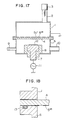
- the ceramic plate 4 in the plasma processing device of Fig. 11 may be vacuum-sealed as shown in Fig. 18. More specifically, an O-ring 13 is sandwitched between the ceramic plate 4 and the plasma production chamber 6 to vacuum-sealed the ceramic plate 4.
- the ceramic plate 4 is provided with slits formed by the gold coating 5 ⁇ and the O-ring selaed surface of the ceramic plate 4 is also plated with gold.
- the O-ring is surrounded by conductor of the gold coating 5 ⁇ and the plasma production chamber 6 and so microwaves don't invade the O-ring. Therefore, the O-ring 13 is not disadvantageously heated by the microwaves.
- the slits shown in Fig. 14 can be formed by the gold (or the like conductor) coating 5 ⁇ on the ceramic plate 4 ⁇ in such a manner as shown in Figs. 19 to 21.
- the lower ceramic plate 5 ⁇ is provided with the continuous gas flow groove 5d ⁇ which are succeeded by the circular gas jet pores 5e ⁇ having a diameter of about 1 mm.
- the gas supplied to the ceramic plate 5 ⁇ is supplied into the plasma production chamber 6 through the gas flow paths the groove 5d ⁇ and the pores 5e ⁇ .
- the upper ceramic plate 4 is, on its lower surface, provided with a slit pattern formed through gold plating (The slits 5c ⁇ are not plated).
- the slit pattern covers the gas flow groove 5d ⁇ of the slit plate 5 ⁇ so that the microwaves don′t invade the groove 5d ⁇ .
- plasma is not created in the grooves 5d ⁇ and the supplied gas is not advantageously decomposed there.
- the slits have been formed by plating the ceramic plate with conductor, these slits may be formed by applying the conductor to the ceramic plate 4 or bonding conductor foil thereto.
- the conductor may be any other conductive any material.
- the slit plate may be preferably made of noble metal such as gold, silver, platinum, etc.
- microwaves are supplied from the magnetron 3 to the cavity resonator 1 in E01 resonance mode through the waveguide 2.
- the waveguide 2 is provided with a choke frange 51 and an insulator 52 which are inserted on the way of the waveguide.
- the waveguide is eccentrically attached to the one side of the cavity resonator 1 so as to provide a desired coupling with the E01 mode.
- On the other side of the cavity resonator 1 attached are in order the ceramic plate 4 and the slit plate 5 having the slits 5c.
- the slit plate 5 is, in the lower side, connected with the plasma production chamber 6 by means of an insulator 53.
- the ceramic plate 4 serves to vacuum-seal the plasma production chamber 6, so that the cavity resonator 1 may be floating and the high frequency power supply 11 may be connected with the cavity resonator 1. Furthermore leakage of microwaves from the waveguide may be prevented.
- a slit plate 55 is provided with the slits 5c located oppositely to the substrate 12.
- the slit plate 55 is, in its periphery, also provided with an inside convex portion 57 and an outside convex portion 59 which are separated from each other by an interval 58.
- the inside convex portion 57 provides a small gap 56 between its tip and the cavity resonator 1.
- the small gap 56 and the interval 58 integral therewith constitute a choke frange 51.
- a ring-shaped insulator 60 is inserted between the tip of the outside convex portion 59 and the cavity resonator 1, so that the cavity resonator 1 may be floating and the high frequency power supply 11 may be connected with the cavity resonator 1. Further more, leakage of microwaves from the waveguide may be prevented.
- the high frequency power supply 11 applies a high frequency voltage to the electrode 7 on which a subtract is placed and the slit plate 55.
- the arrangement according to this embodiment can perform the cleaning of the slit plate 55 and the electrode 7 in addition to the plasma processing. More specifically, processing gas of CF4 is introduced from the gas supply tube 9 into the plasma production chamber 6. When a high frequency voltage is applied from the high frequency power supply 11 to the slit plate 55 by the switch 61, the energy of the ions from the plasma is increased, thereby cleaning the slit plate 55 at high speed. Similarly, when the high frequency voltage is applied to the electrode 7, the electrode can be plasma-cleaned. High frequency power supplies may be provided individually for the slit plate 55 and the electrode as shown by dotted lines.
Landscapes
- Chemical & Material Sciences (AREA)
- Engineering & Computer Science (AREA)
- Physics & Mathematics (AREA)
- Plasma & Fusion (AREA)
- Analytical Chemistry (AREA)
- General Chemical & Material Sciences (AREA)
- Chemical Kinetics & Catalysis (AREA)
- Materials Engineering (AREA)
- Mechanical Engineering (AREA)
- Metallurgy (AREA)
- Organic Chemistry (AREA)
- Drying Of Semiconductors (AREA)
Applications Claiming Priority (8)
| Application Number | Priority Date | Filing Date | Title |
|---|---|---|---|
| JP247412/86 | 1986-10-20 | ||
| JP24741286A JP2569019B2 (ja) | 1986-10-20 | 1986-10-20 | エッチング方法及びその装置 |
| JP62068838A JP2633849B2 (ja) | 1987-03-25 | 1987-03-25 | プラズマ処理装置 |
| JP68838/87 | 1987-03-25 | ||
| JP62097525A JP2662219B2 (ja) | 1987-04-22 | 1987-04-22 | プラズマ処理装置 |
| JP97525/87 | 1987-04-22 | ||
| JP62128158A JP2675000B2 (ja) | 1987-05-27 | 1987-05-27 | プラズマ処理装置 |
| JP128158/87 | 1987-05-27 |
Publications (3)
| Publication Number | Publication Date |
|---|---|
| EP0264913A2 true EP0264913A2 (de) | 1988-04-27 |
| EP0264913A3 EP0264913A3 (en) | 1989-09-06 |
| EP0264913B1 EP0264913B1 (de) | 1994-06-22 |
Family
ID=27465045
Family Applications (1)
| Application Number | Title | Priority Date | Filing Date |
|---|---|---|---|
| EP87115349A Expired - Lifetime EP0264913B1 (de) | 1986-10-20 | 1987-10-20 | Plasmabearbeitungsgerät |
Country Status (3)
| Country | Link |
|---|---|
| US (1) | US4776918A (de) |
| EP (1) | EP0264913B1 (de) |
| DE (1) | DE3750115T2 (de) |
Cited By (16)
| Publication number | Priority date | Publication date | Assignee | Title |
|---|---|---|---|---|
| EP0295083A3 (de) * | 1987-06-08 | 1989-08-02 | Efthimion, Philip C., Dr. | Apparat und Verfahren für chemische Behandlungen mittels Hochdruck- und Atmosphärendruckplasma, hergestellt durch elektromagnetischen Wellen hoher Frequenz |
| EP0343602A3 (de) * | 1988-05-25 | 1991-01-09 | Canon Kabushiki Kaisha | Mikrowellen-Plasma-Bearbeitungsgerät |
| EP0421348A1 (de) * | 1989-10-06 | 1991-04-10 | Hitachi, Ltd. | Anlage zur Herstellung von Schichten |
| EP0382065A3 (de) * | 1989-02-08 | 1991-07-17 | Hitachi, Ltd. | Plasma-Bearbeitungsgerät |
| EP0477906A3 (en) * | 1990-09-28 | 1992-05-06 | Hitachi, Ltd. | Plasma processing apparatus using plasma produced by microwaves |
| EP0462209A4 (en) * | 1989-03-09 | 1992-07-29 | Applied Microwave Plasma Concepts, Inc. | Electron cyclotron resonance plasma source and method of operation |
| EP0554039A1 (de) * | 1992-01-30 | 1993-08-04 | Hitachi, Ltd. | Verfahren und Vorrichtung zur Plasmaerzeugung und Verfahren zur Halbleiter-Bearbeitung |
| EP0653775A1 (de) * | 1993-11-12 | 1995-05-17 | Hitachi, Ltd. | Mikrowellenplasma-Bearbeitungsvorrichtung und -verfahren |
| EP0737256A4 (de) * | 1993-06-04 | 1996-12-27 | Applied Science Technology | Mikrowellenplasmareaktor |
| GB2315918A (en) * | 1996-07-30 | 1998-02-11 | Nec Corp | Plasma treatment apparatus |
| EP0880164A1 (de) * | 1997-05-22 | 1998-11-25 | Canon Kabushiki Kaisha | Plasmabehandlungsvorrichtung mit einem mit ringförmigem Wellenleiter versehenen Mikrowellenauftragsgerät und Behandlungsverfahren |
| US6299691B1 (en) | 1999-01-28 | 2001-10-09 | Canon Kabushiki Kaisha | Method of and apparatus for processing a substrate under a reduced pressure |
| EP0688038B1 (de) * | 1994-06-14 | 2001-12-19 | Sumitomo Metal Industries, Ltd. | Mikrowellenplasma-Bearbeitungssystem |
| CN102737944A (zh) * | 2011-03-31 | 2012-10-17 | 东京毅力科创株式会社 | 等离子体处理装置和等离子体产生用天线 |
| EP2720518B1 (de) * | 2011-06-09 | 2016-12-28 | Korea Basic Science Institute | Plasmaerzeugungsquelle mit einem bandförmigen magneten und dünnfilmabscheidungssystem damit |
| WO2021181102A1 (en) * | 2020-03-12 | 2021-09-16 | Lancaster University | Improvements in and relating to plasma furnaces |
Families Citing this family (75)
| Publication number | Priority date | Publication date | Assignee | Title |
|---|---|---|---|---|
| US5308431A (en) * | 1986-04-18 | 1994-05-03 | General Signal Corporation | System providing multiple processing of substrates |
| US5102495A (en) * | 1986-04-18 | 1992-04-07 | General Signal Corporation | Method providing multiple-processing of substrates |
| US6103055A (en) * | 1986-04-18 | 2000-08-15 | Applied Materials, Inc. | System for processing substrates |
| CA1331163C (en) * | 1986-04-18 | 1994-08-02 | Applied Materials, Inc. | Multiple-processing and contamination-free plasma etching system |
| EP0267513B1 (de) * | 1986-11-10 | 1998-08-12 | Semiconductor Energy Laboratory Co., Ltd. | Durch Mikrowellen gesteigertes CVD-Verfahren und -Gerät |
| US6677001B1 (en) * | 1986-11-10 | 2004-01-13 | Semiconductor Energy Laboratory Co., Ltd. | Microwave enhanced CVD method and apparatus |
| US5433788A (en) * | 1987-01-19 | 1995-07-18 | Hitachi, Ltd. | Apparatus for plasma treatment using electron cyclotron resonance |
| EP0288065B1 (de) * | 1987-04-22 | 1993-10-06 | Idemitsu Petrochemical Co. Ltd. | Verfahren zur Diamantsynthese |
| US4926791A (en) * | 1987-04-27 | 1990-05-22 | Semiconductor Energy Laboratory Co., Ltd. | Microwave plasma apparatus employing helmholtz coils and ioffe bars |
| JPH0754759B2 (ja) * | 1987-04-27 | 1995-06-07 | 日本電信電話株式会社 | プラズマ処理方法および装置並びにプラズマ処理装置用モード変換器 |
| KR920002864B1 (ko) * | 1987-07-20 | 1992-04-06 | 가부시기가이샤 히다찌세이사꾸쇼 | 플라즈마 처리방법 및 그 장치 |
| JPS6424094A (en) * | 1987-07-21 | 1989-01-26 | Nat Inst Res Inorganic Mat | Synthesizing apparatus for diamond |
| KR910007384B1 (ko) * | 1987-09-16 | 1991-09-25 | 가부시끼가이샤 한도다이 에네르기 겐뀨쇼 | 초전도 산화물 형성방법 및 장치 |
| US4911812A (en) * | 1987-10-21 | 1990-03-27 | Hitachi, Ltd. | Plasma treating method and apparatus therefor |
| GB2212974B (en) * | 1987-11-25 | 1992-02-12 | Fuji Electric Co Ltd | Plasma processing apparatus |
| US5024716A (en) * | 1988-01-20 | 1991-06-18 | Canon Kabushiki Kaisha | Plasma processing apparatus for etching, ashing and film-formation |
| US4893584A (en) * | 1988-03-29 | 1990-01-16 | Energy Conversion Devices, Inc. | Large area microwave plasma apparatus |
| KR910002310A (ko) * | 1988-06-29 | 1991-01-31 | 미다 가쓰시게 | 플라즈마 처리장치 |
| JPH0216732A (ja) * | 1988-07-05 | 1990-01-19 | Mitsubishi Electric Corp | プラズマ反応装置 |
| JPH0227718A (ja) * | 1988-07-15 | 1990-01-30 | Mitsubishi Electric Corp | プラズマ処理方法およびそれに用いるプラズマ処理装置 |
| DE3843098A1 (de) * | 1988-12-21 | 1990-06-28 | Technics Plasma Gmbh | Verfahren und vorrichtung zur kunststoffbeschichtung von strangprofilen |
| DE3903322A1 (de) * | 1989-02-04 | 1990-08-16 | Nmi Naturwissenschaftl U Mediz | Verfahren zur erzeugung von ionen |
| US5370765A (en) * | 1989-03-09 | 1994-12-06 | Applied Microwave Plasma Concepts, Inc. | Electron cyclotron resonance plasma source and method of operation |
| US5032205A (en) * | 1989-05-05 | 1991-07-16 | Wisconsin Alumni Research Foundation | Plasma etching apparatus with surface magnetic fields |
| US5225024A (en) * | 1989-05-08 | 1993-07-06 | Applied Materials, Inc. | Magnetically enhanced plasma reactor system for semiconductor processing |
| US5091049A (en) * | 1989-06-13 | 1992-02-25 | Plasma & Materials Technologies, Inc. | High density plasma deposition and etching apparatus |
| US5134965A (en) * | 1989-06-16 | 1992-08-04 | Hitachi, Ltd. | Processing apparatus and method for plasma processing |
| US5312778A (en) * | 1989-10-03 | 1994-05-17 | Applied Materials, Inc. | Method for plasma processing using magnetically enhanced plasma chemical vapor deposition |
| JP2602336B2 (ja) * | 1989-11-29 | 1997-04-23 | 株式会社日立製作所 | プラズマ処理装置 |
| US5013400A (en) * | 1990-01-30 | 1991-05-07 | General Signal Corporation | Dry etch process for forming champagne profiles, and dry etch apparatus |
| JP2581255B2 (ja) * | 1990-04-02 | 1997-02-12 | 富士電機株式会社 | プラズマ処理方法 |
| JP3056772B2 (ja) * | 1990-08-20 | 2000-06-26 | 株式会社日立製作所 | プラズマの制御方法ならびにプラズマ処理方法およびその装置 |
| KR930011413B1 (ko) | 1990-09-25 | 1993-12-06 | 가부시키가이샤 한도오따이 에네루기 겐큐쇼 | 펄스형 전자파를 사용한 플라즈마 cvd 법 |
| US5804033A (en) * | 1990-09-26 | 1998-09-08 | Hitachi, Ltd. | Microwave plasma processing method and apparatus |
| DE4119362A1 (de) * | 1991-06-12 | 1992-12-17 | Leybold Ag | Teilchenquelle, insbesondere fuer reaktive ionenaetz- und plasmaunterstuetzte cvd-verfahren |
| US5628883A (en) * | 1991-06-18 | 1997-05-13 | Japan Vilene Co. Ltd. | Method for generating and activating plasma process of treatment using same, and apparatus therefor |
| JP3042127B2 (ja) * | 1991-09-02 | 2000-05-15 | 富士電機株式会社 | 酸化シリコン膜の製造方法および製造装置 |
| JP3158715B2 (ja) * | 1992-03-30 | 2001-04-23 | 株式会社ダイヘン | プラズマ処理装置 |
| JP2570090B2 (ja) * | 1992-10-08 | 1997-01-08 | 日本電気株式会社 | ドライエッチング装置 |
| US5248371A (en) * | 1992-08-13 | 1993-09-28 | General Signal Corporation | Hollow-anode glow discharge apparatus |
| DE4230291C2 (de) * | 1992-09-10 | 1999-11-04 | Leybold Ag | Mikrowellenunterstützte Zerstäubungsanordnung |
| US5537004A (en) * | 1993-03-06 | 1996-07-16 | Tokyo Electron Limited | Low frequency electron cyclotron resonance plasma processor |
| US5662770A (en) * | 1993-04-16 | 1997-09-02 | Micron Technology, Inc. | Method and apparatus for improving etch uniformity in remote source plasma reactors with powered wafer chucks |
| JPH0987851A (ja) * | 1995-09-21 | 1997-03-31 | Canon Inc | マイクロ波プラズマ処理装置及び処理方法 |
| JPH09125243A (ja) * | 1995-10-27 | 1997-05-13 | Canon Inc | 薄膜形成装置 |
| JPH09129607A (ja) * | 1995-11-01 | 1997-05-16 | Canon Inc | マイクロ波プラズマエッチング装置及び方法 |
| US5803975A (en) * | 1996-03-01 | 1998-09-08 | Canon Kabushiki Kaisha | Microwave plasma processing apparatus and method therefor |
| JPH09266096A (ja) | 1996-03-28 | 1997-10-07 | Hitachi Ltd | プラズマ処理装置及びこれを用いたプラズマ処理方法 |
| GB9712338D0 (en) | 1997-06-14 | 1997-08-13 | Secr Defence | Surface coatings |
| US6368988B1 (en) | 1999-07-16 | 2002-04-09 | Micron Technology, Inc. | Combined gate cap or digit line and spacer deposition using HDP |
| JP2001203099A (ja) | 2000-01-20 | 2001-07-27 | Yac Co Ltd | プラズマ生成装置およびプラズマ処理装置 |
| US6677549B2 (en) * | 2000-07-24 | 2004-01-13 | Canon Kabushiki Kaisha | Plasma processing apparatus having permeable window covered with light shielding film |
| DE10114115A1 (de) * | 2001-03-22 | 2002-10-02 | Muegge Electronic Gmbh | Anordnung zur Erzeugung von Plasma in einem Behandlungsraum |
| JP4183934B2 (ja) * | 2001-10-19 | 2008-11-19 | 尚久 後藤 | マイクロ波プラズマ処理装置、マイクロ波プラズマ処理方法及びマイクロ波給電装置 |
| US6988380B2 (en) * | 2002-08-15 | 2006-01-24 | Ceramoptec Industries, Inc. | Method of silica optical fiber preform production |
| US6928839B2 (en) * | 2002-08-15 | 2005-08-16 | Ceramoptec Industries, Inc. | Method for production of silica optical fiber preforms |
| JP4381001B2 (ja) * | 2003-02-25 | 2009-12-09 | シャープ株式会社 | プラズマプロセス装置 |
| US20050178333A1 (en) * | 2004-02-18 | 2005-08-18 | Asm Japan K.K. | System and method of CVD chamber cleaning |
| GB0406049D0 (en) * | 2004-03-18 | 2004-04-21 | Secr Defence | Surface coatings |
| DE102004030344B4 (de) * | 2004-06-18 | 2012-12-06 | Carl Zeiss | Vorrichtung zum Beschichten optischer Gläser mittels plasmaunterstützter chemischer Dampfabscheidung (CVD) |
| EP1739717A1 (de) * | 2005-06-30 | 2007-01-03 | Alter S.r.l. | Plasmagenerator mit einer Schlitzantenne |
| US7485827B2 (en) * | 2006-07-21 | 2009-02-03 | Alter S.R.L. | Plasma generator |
| EP2108714B1 (de) * | 2007-01-29 | 2014-03-12 | Sumitomo Electric Industries, Ltd. | Mikrowellen-plasma-cvd-system |
| JP4793662B2 (ja) * | 2008-03-28 | 2011-10-12 | 独立行政法人産業技術総合研究所 | マイクロ波プラズマ処理装置 |
| EP2230881B1 (de) * | 2009-03-20 | 2018-11-28 | Whirlpool Corporation | Mikrowellenheizvorrichtung |
| JP5457754B2 (ja) * | 2009-08-07 | 2014-04-02 | 株式会社日立ハイテクノロジーズ | 透過型電極体を用いたプラズマ処理装置 |
| JP5632186B2 (ja) * | 2010-04-20 | 2014-11-26 | 株式会社日立ハイテクノロジーズ | 稠密スロット透過型電極体を用いたプラズマ処理装置 |
| WO2011137371A2 (en) | 2010-04-30 | 2011-11-03 | Applied Materials, Inc. | Vertical inline cvd system |
| JP2014026773A (ja) * | 2012-07-25 | 2014-02-06 | Tokyo Electron Ltd | プラズマ処理装置 |
| JP6144902B2 (ja) | 2012-12-10 | 2017-06-07 | 東京エレクトロン株式会社 | マイクロ波放射アンテナ、マイクロ波プラズマ源およびプラズマ処理装置 |
| US9793095B2 (en) * | 2013-03-14 | 2017-10-17 | Tokyo Electron Limited | Microwave surface-wave plasma device |
| US9941126B2 (en) * | 2013-06-19 | 2018-04-10 | Tokyo Electron Limited | Microwave plasma device |
| WO2015069905A1 (en) * | 2013-11-06 | 2015-05-14 | Tokyo Electron Limited | Multi-cell resonator microwave surface-wave plasma apparatus |
| JP6356415B2 (ja) | 2013-12-16 | 2018-07-11 | 東京エレクトロン株式会社 | マイクロ波プラズマ源およびプラズマ処理装置 |
| JP7330391B2 (ja) * | 2021-06-28 | 2023-08-21 | 株式会社日立ハイテク | プラズマ処理装置及びプラズマ処理方法 |
Family Cites Families (6)
| Publication number | Priority date | Publication date | Assignee | Title |
|---|---|---|---|---|
| JPS55134175A (en) * | 1979-04-06 | 1980-10-18 | Hitachi Ltd | Microwave plasma etching unit |
| JPS5613480A (en) * | 1979-07-13 | 1981-02-09 | Hitachi Ltd | Dry etching apparatus |
| JPS5696841A (en) * | 1979-12-28 | 1981-08-05 | Fujitsu Ltd | Microwave plasma treating apparatus |
| EP0103461B1 (de) * | 1982-09-10 | 1988-11-17 | Nippon Telegraph And Telephone Corporation | Vorrichtung und Verfahren zum Auftragen mittels Plasma |
| EP0173164B1 (de) * | 1984-08-31 | 1988-11-09 | Hitachi, Ltd. | Aufstäuben mittels Mikrowellen |
| JPS61131454A (ja) * | 1984-11-30 | 1986-06-19 | Fujitsu Ltd | マイクロ波プラズマ処理方法と装置 |
-
1987
- 1987-10-20 EP EP87115349A patent/EP0264913B1/de not_active Expired - Lifetime
- 1987-10-20 US US07/110,368 patent/US4776918A/en not_active Expired - Lifetime
- 1987-10-20 DE DE3750115T patent/DE3750115T2/de not_active Expired - Fee Related
Cited By (22)
| Publication number | Priority date | Publication date | Assignee | Title |
|---|---|---|---|---|
| EP0295083A3 (de) * | 1987-06-08 | 1989-08-02 | Efthimion, Philip C., Dr. | Apparat und Verfahren für chemische Behandlungen mittels Hochdruck- und Atmosphärendruckplasma, hergestellt durch elektromagnetischen Wellen hoher Frequenz |
| EP0343602A3 (de) * | 1988-05-25 | 1991-01-09 | Canon Kabushiki Kaisha | Mikrowellen-Plasma-Bearbeitungsgerät |
| EP0382065A3 (de) * | 1989-02-08 | 1991-07-17 | Hitachi, Ltd. | Plasma-Bearbeitungsgerät |
| EP0462209A4 (en) * | 1989-03-09 | 1992-07-29 | Applied Microwave Plasma Concepts, Inc. | Electron cyclotron resonance plasma source and method of operation |
| EP0421348A1 (de) * | 1989-10-06 | 1991-04-10 | Hitachi, Ltd. | Anlage zur Herstellung von Schichten |
| EP0477906A3 (en) * | 1990-09-28 | 1992-05-06 | Hitachi, Ltd. | Plasma processing apparatus using plasma produced by microwaves |
| US5646489A (en) * | 1992-01-30 | 1997-07-08 | Hitachi, Ltd. | Plasma generator with mode restricting means |
| US5433789A (en) * | 1992-01-30 | 1995-07-18 | Hitachi, Ltd. | Methods and apparatus for generating plasma, and semiconductor processing methods using mode restricted microwaves |
| EP0554039A1 (de) * | 1992-01-30 | 1993-08-04 | Hitachi, Ltd. | Verfahren und Vorrichtung zur Plasmaerzeugung und Verfahren zur Halbleiter-Bearbeitung |
| EP0737256A4 (de) * | 1993-06-04 | 1996-12-27 | Applied Science Technology | Mikrowellenplasmareaktor |
| EP0653775A1 (de) * | 1993-11-12 | 1995-05-17 | Hitachi, Ltd. | Mikrowellenplasma-Bearbeitungsvorrichtung und -verfahren |
| EP0688038B1 (de) * | 1994-06-14 | 2001-12-19 | Sumitomo Metal Industries, Ltd. | Mikrowellenplasma-Bearbeitungssystem |
| US5988104A (en) * | 1996-07-30 | 1999-11-23 | Nec Corporation | Plasma treatment system |
| GB2315918B (en) * | 1996-07-30 | 2001-07-18 | Nec Corp | Plasma treatment system |
| GB2315918A (en) * | 1996-07-30 | 1998-02-11 | Nec Corp | Plasma treatment apparatus |
| EP0880164A1 (de) * | 1997-05-22 | 1998-11-25 | Canon Kabushiki Kaisha | Plasmabehandlungsvorrichtung mit einem mit ringförmigem Wellenleiter versehenen Mikrowellenauftragsgerät und Behandlungsverfahren |
| US6497783B1 (en) | 1997-05-22 | 2002-12-24 | Canon Kabushiki Kaisha | Plasma processing apparatus provided with microwave applicator having annular waveguide and processing method |
| US6299691B1 (en) | 1999-01-28 | 2001-10-09 | Canon Kabushiki Kaisha | Method of and apparatus for processing a substrate under a reduced pressure |
| CN102737944A (zh) * | 2011-03-31 | 2012-10-17 | 东京毅力科创株式会社 | 等离子体处理装置和等离子体产生用天线 |
| US9543123B2 (en) | 2011-03-31 | 2017-01-10 | Tokyo Electronics Limited | Plasma processing apparatus and plasma generation antenna |
| EP2720518B1 (de) * | 2011-06-09 | 2016-12-28 | Korea Basic Science Institute | Plasmaerzeugungsquelle mit einem bandförmigen magneten und dünnfilmabscheidungssystem damit |
| WO2021181102A1 (en) * | 2020-03-12 | 2021-09-16 | Lancaster University | Improvements in and relating to plasma furnaces |
Also Published As
| Publication number | Publication date |
|---|---|
| DE3750115T2 (de) | 1995-01-19 |
| DE3750115D1 (de) | 1994-07-28 |
| EP0264913A3 (en) | 1989-09-06 |
| EP0264913B1 (de) | 1994-06-22 |
| US4776918A (en) | 1988-10-11 |
Similar Documents
| Publication | Publication Date | Title |
|---|---|---|
| US4776918A (en) | Plasma processing apparatus | |
| KR100497015B1 (ko) | 플라즈마 처리 장치, 플라즈마 처리 방법 및 지파판 | |
| EP0237078B1 (de) | Anordnung zur Stromab-Bearbeitung mit mikrowellenerzeugtem Plasma mit Kopplungsstruktur zwischen Mikrowellen und Plasma | |
| EP0379828B1 (de) | Radiofrequenzinduktion/Mehrpolplasma-Bearbeitungsvorrichtung | |
| US4610770A (en) | Method and apparatus for sputtering | |
| KR920002864B1 (ko) | 플라즈마 처리방법 및 그 장치 | |
| EP0217361B1 (de) | Ionenquelle | |
| US6427621B1 (en) | Plasma processing device and plasma processing method | |
| EP0591975B1 (de) | Trockenätzgerät von Typ mit zwei parallel verlaufende Flachelektroden | |
| KR100269552B1 (ko) | 플라즈마 처리 장치 | |
| KR20030004426A (ko) | 플라즈마 처리 장치 | |
| JPH01184923A (ja) | プラズマ処理装置及びプラズマ処理方法 | |
| JP2569019B2 (ja) | エッチング方法及びその装置 | |
| US7779783B2 (en) | Plasma processing device | |
| JP2662219B2 (ja) | プラズマ処理装置 | |
| KR100785960B1 (ko) | 플라즈마 처리 장치 | |
| JPH09171900A (ja) | プラズマ発生装置 | |
| JP2800766B2 (ja) | プラズマ処理方法及びその装置 | |
| JP2675000B2 (ja) | プラズマ処理装置 | |
| JP2633849B2 (ja) | プラズマ処理装置 | |
| US6432730B2 (en) | Plasma processing method and apparatus | |
| JP2641450B2 (ja) | プラズマ処理装置 | |
| JP2738810B2 (ja) | プラズマ処理装置 | |
| JP2666697B2 (ja) | マイクロ波プラズマ処理装置 | |
| JP3208995B2 (ja) | プラズマ処理方法及び装置 |
Legal Events
| Date | Code | Title | Description |
|---|---|---|---|
| PUAI | Public reference made under article 153(3) epc to a published international application that has entered the european phase |
Free format text: ORIGINAL CODE: 0009012 |
|
| AK | Designated contracting states |
Kind code of ref document: A2 Designated state(s): DE FR GB |
|
| PUAL | Search report despatched |
Free format text: ORIGINAL CODE: 0009013 |
|
| AK | Designated contracting states |
Kind code of ref document: A3 Designated state(s): DE FR GB |
|
| 17P | Request for examination filed |
Effective date: 19890908 |
|
| 17Q | First examination report despatched |
Effective date: 19911016 |
|
| GRAA | (expected) grant |
Free format text: ORIGINAL CODE: 0009210 |
|
| AK | Designated contracting states |
Kind code of ref document: B1 Designated state(s): DE FR GB |
|
| REF | Corresponds to: |
Ref document number: 3750115 Country of ref document: DE Date of ref document: 19940728 |
|
| ET | Fr: translation filed | ||
| PLBE | No opposition filed within time limit |
Free format text: ORIGINAL CODE: 0009261 |
|
| STAA | Information on the status of an ep patent application or granted ep patent |
Free format text: STATUS: NO OPPOSITION FILED WITHIN TIME LIMIT |
|
| 26N | No opposition filed | ||
| PGFP | Annual fee paid to national office [announced via postgrant information from national office to epo] |
Ref country code: FR Payment date: 19960814 Year of fee payment: 10 |
|
| PG25 | Lapsed in a contracting state [announced via postgrant information from national office to epo] |
Ref country code: FR Free format text: THE PATENT HAS BEEN ANNULLED BY A DECISION OF A NATIONAL AUTHORITY Effective date: 19971031 |
|
| REG | Reference to a national code |
Ref country code: FR Ref legal event code: ST |
|
| REG | Reference to a national code |
Ref country code: GB Ref legal event code: IF02 |
|
| PGFP | Annual fee paid to national office [announced via postgrant information from national office to epo] |
Ref country code: GB Payment date: 20040923 Year of fee payment: 18 |
|
| PGFP | Annual fee paid to national office [announced via postgrant information from national office to epo] |
Ref country code: DE Payment date: 20041206 Year of fee payment: 18 |
|
| PG25 | Lapsed in a contracting state [announced via postgrant information from national office to epo] |
Ref country code: GB Free format text: LAPSE BECAUSE OF NON-PAYMENT OF DUE FEES Effective date: 20051020 |
|
| PG25 | Lapsed in a contracting state [announced via postgrant information from national office to epo] |
Ref country code: DE Free format text: LAPSE BECAUSE OF NON-PAYMENT OF DUE FEES Effective date: 20060503 |
|
| GBPC | Gb: european patent ceased through non-payment of renewal fee |
Effective date: 20051020 |