EP0265367A1 - Disposition de plots de contact à largeur variable - Google Patents
Disposition de plots de contact à largeur variable Download PDFInfo
- Publication number
- EP0265367A1 EP0265367A1 EP87630206A EP87630206A EP0265367A1 EP 0265367 A1 EP0265367 A1 EP 0265367A1 EP 87630206 A EP87630206 A EP 87630206A EP 87630206 A EP87630206 A EP 87630206A EP 0265367 A1 EP0265367 A1 EP 0265367A1
- Authority
- EP
- European Patent Office
- Prior art keywords
- pad
- bond
- center
- pads
- bond pad
- Prior art date
- Legal status (The legal status is an assumption and is not a legal conclusion. Google has not performed a legal analysis and makes no representation as to the accuracy of the status listed.)
- Granted
Links
Images


Classifications
-
- H—ELECTRICITY
- H10—SEMICONDUCTOR DEVICES; ELECTRIC SOLID-STATE DEVICES NOT OTHERWISE PROVIDED FOR
- H10W—GENERIC PACKAGES, INTERCONNECTIONS, CONNECTORS OR OTHER CONSTRUCTIONAL DETAILS OF DEVICES COVERED BY CLASS H10
- H10W70/00—Package substrates; Interposers; Redistribution layers [RDL]
- H10W70/60—Insulating or insulated package substrates; Interposers; Redistribution layers
- H10W70/62—Insulating or insulated package substrates; Interposers; Redistribution layers characterised by their interconnections
- H10W70/65—Shapes or dispositions of interconnections
-
- H—ELECTRICITY
- H05—ELECTRIC TECHNIQUES NOT OTHERWISE PROVIDED FOR
- H05K—PRINTED CIRCUITS; CASINGS OR CONSTRUCTIONAL DETAILS OF ELECTRIC APPARATUS; MANUFACTURE OF ASSEMBLAGES OF ELECTRICAL COMPONENTS
- H05K1/00—Printed circuits
- H05K1/02—Details
- H05K1/11—Printed elements for providing electric connections to or between printed circuits
- H05K1/111—Pads for surface mounting, e.g. lay-out
-
- H—ELECTRICITY
- H10—SEMICONDUCTOR DEVICES; ELECTRIC SOLID-STATE DEVICES NOT OTHERWISE PROVIDED FOR
- H10W—GENERIC PACKAGES, INTERCONNECTIONS, CONNECTORS OR OTHER CONSTRUCTIONAL DETAILS OF DEVICES COVERED BY CLASS H10
- H10W70/00—Package substrates; Interposers; Redistribution layers [RDL]
- H10W70/01—Manufacture or treatment
- H10W70/05—Manufacture or treatment of insulating or insulated package substrates, or of interposers, or of redistribution layers
-
- H—ELECTRICITY
- H05—ELECTRIC TECHNIQUES NOT OTHERWISE PROVIDED FOR
- H05K—PRINTED CIRCUITS; CASINGS OR CONSTRUCTIONAL DETAILS OF ELECTRIC APPARATUS; MANUFACTURE OF ASSEMBLAGES OF ELECTRICAL COMPONENTS
- H05K1/00—Printed circuits
- H05K1/02—Details
- H05K1/03—Use of materials for the substrate
- H05K1/0306—Inorganic insulating substrates, e.g. ceramic, glass
-
- H—ELECTRICITY
- H05—ELECTRIC TECHNIQUES NOT OTHERWISE PROVIDED FOR
- H05K—PRINTED CIRCUITS; CASINGS OR CONSTRUCTIONAL DETAILS OF ELECTRIC APPARATUS; MANUFACTURE OF ASSEMBLAGES OF ELECTRICAL COMPONENTS
- H05K2201/00—Indexing scheme relating to printed circuits covered by H05K1/00
- H05K2201/09—Shape and layout
- H05K2201/09209—Shape and layout details of conductors
- H05K2201/09372—Pads and lands
- H05K2201/094—Array of pads or lands differing from one another, e.g. in size, pitch or thickness; Using different connections on the pads
-
- H—ELECTRICITY
- H05—ELECTRIC TECHNIQUES NOT OTHERWISE PROVIDED FOR
- H05K—PRINTED CIRCUITS; CASINGS OR CONSTRUCTIONAL DETAILS OF ELECTRIC APPARATUS; MANUFACTURE OF ASSEMBLAGES OF ELECTRICAL COMPONENTS
- H05K2201/00—Indexing scheme relating to printed circuits covered by H05K1/00
- H05K2201/10—Details of components or other objects attached to or integrated in a printed circuit board
- H05K2201/10613—Details of electrical connections of non-printed components, e.g. special leads
- H05K2201/10621—Components characterised by their electrical contacts
- H05K2201/10681—Tape Carrier Package [TCP]; Flexible sheet connector
-
- H—ELECTRICITY
- H05—ELECTRIC TECHNIQUES NOT OTHERWISE PROVIDED FOR
- H05K—PRINTED CIRCUITS; CASINGS OR CONSTRUCTIONAL DETAILS OF ELECTRIC APPARATUS; MANUFACTURE OF ASSEMBLAGES OF ELECTRICAL COMPONENTS
- H05K3/00—Apparatus or processes for manufacturing printed circuits
- H05K3/30—Assembling printed circuits with electric components, e.g. with resistors
- H05K3/32—Assembling printed circuits with electric components, e.g. with resistors electrically connecting electric components or wires to printed circuits
- H05K3/34—Assembling printed circuits with electric components, e.g. with resistors electrically connecting electric components or wires to printed circuits by soldering
- H05K3/341—Surface mounted components
- H05K3/3421—Leaded components
-
- Y—GENERAL TAGGING OF NEW TECHNOLOGICAL DEVELOPMENTS; GENERAL TAGGING OF CROSS-SECTIONAL TECHNOLOGIES SPANNING OVER SEVERAL SECTIONS OF THE IPC; TECHNICAL SUBJECTS COVERED BY FORMER USPC CROSS-REFERENCE ART COLLECTIONS [XRACs] AND DIGESTS
- Y02—TECHNOLOGIES OR APPLICATIONS FOR MITIGATION OR ADAPTATION AGAINST CLIMATE CHANGE
- Y02P—CLIMATE CHANGE MITIGATION TECHNOLOGIES IN THE PRODUCTION OR PROCESSING OF GOODS
- Y02P70/00—Climate change mitigation technologies in the production process for final industrial or consumer products
- Y02P70/50—Manufacturing or production processes characterised by the final manufactured product
Definitions
- This invention relates to integrated circuit (IC) packaging, and more particularly to ceramic IC packages.
- the manufacture of ceramic microelectronic packages by the co-firing process involves deposition of trace refractory metallization on the unfired, or "green" tape cast of the ceramic IC carrier.
- the trace metal represents the package bond pads which the IC die leads attach to.
- the firing of the green tape shrinks the ceramic to a final, post-fired size.
- the shrinkage is predictable (on the order of 18%) to within a +/-"acceptable variation" tolerance.
- the standard variation tolerance is +/- 1.0 % of the nominal post-fired ceramic body dimension.
- the trace metal also shrinks predictably when the ceramic is fired, with the same +/- 1.0 % variation tolerance on size and geometrical spacing. If a first array of trace line metal is deposited on the green tape ceramic and is intended for post-fired registration with a second array of trace metal having a nominal dimension of 1.0 inches, then the final dimension of the first array may be 1.000 +/- 0.010 inches.
- Prior art methods of mounting the IC dies to the ceramic package bond pads include both manual and automated bonding processes.
- the electrical interconnection of the IC to the package require operator alignment of the IC interconnect wires (or ribbon) to the bond pads. After alignment a bonder machine secures the device leads to the bond pads by welding or soldering.
- Automated processes such as tape automated bonding (TAB), require accurate positioning of the package bond pads so as to automatically receive the IC TAB leads in register. The +/- 1.0 % shrinkage tolerance creates problems with the TAB to bond pad registration.
- bond pads may be made large enough to accommodate all manufacturing tolerances, including the shrinkage tolerance, this prevents increasing package density.
- the IC industry drive towards miniaturization requires high density packaging which prohibits this brute force method of lead registration.
- the object of the present invention is to provide a method of designing the widths of the bond pad trace metallization deposited on a pre-fired ceramic package so as to ensure automatic post-fired registration of the package bond pads with the IC device TAB leads.
- the bond pad metallization for a ceramic package is deposited on the pre-fired ceramic with the bond pad widths increasing as a function of the distance of each pad from the center of package mass toward which the ceramic shinkage takes place, whereby bond pads at the extremity of the package have the largest pad width and pads toward the center of the package have the narrowest width.
- the widths of the package bond pads which are furthest from the center of package mass are made wider than those pads closest to the center.
- the greater the distance from the center of mass the greater the effect of the feature displacement due to the +/- 1.0% tolerance. Since the furthest bond pads experience the greatest shrinkage tolerance variation, and resultant feature displacement, increasing their width ensures their registration with the IC TAB leads under the worst case conditions of the post-fired tolerance.
- the bond pads closest to the center of package mass are deposited with the smallest widths. Since the closer pads experience the minimum shrinkage tolerance variation, and resultant minimum feature displacement, the narrower widths still ensure registration with the IC leads. Instead of making all of the bond pads uniformly wide the actual width of each pad varies with the pad's location from the package center of mass.
- the present invention takes advantage of the fact that ceramic shrinkage with firing is not constant across the ceramic body. Instead, the different areas of the ceramic body shrink by a percentage dependent on the distance of the area from the center of mass. The amount of shrinkage is greater at the periphery, and decreases from the outer edges towards the center of the body in a more or less predetermined fashion, subject to the +/-1.0% tolerance.
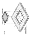
- Fig. 2 illustrates a standard, leadless ceramic package (chip carrier) 10 in which the present invention may be used.
- the package includes a substrate 11, having a symmetrical central cavity 12.
- the cavity is stepped, to provide a bond shelf 13 having an outer dimension Dc and an inner dimension D d .
- the Dd dimension is larger than that of a silicon IC die 14 to be mounted in the package.
- the die is mounted to a tape 16 using a tape automated bonding (TAB) process known in the art.
- TAB tape automated bonding
- the tape connects the die terminals to input/output (I/O) TAB leads 18.
- the TAB leads have a lead width (T w ) 20.
- the tape-mounted die is fitted into the lower part of the cavity, with registration of the IC TAB leads 18 to the package bond pads 22 arrayed along the bond pad shelf 13; on all four sides of the cavity 12.
- the TAB leads are welded, or soldered to the package bond pads.
- the bond pads 22 are connected (not shown) through the substrate 11 to corresponding outer bond pads 26, which allow connection of the IC to user equipment outside the package.
- the IC TAB process, the fabrication of the ceramic package, the deposition of the bond pad metallization, and the mounting of the IC to the package, are all accomplished through known, prior art methods.
- the bond pads may be deposited using any one of a number of known deposition techniques, i.e. photolithographic deposition. They are not a part of the present invention.
- the present invention relates to the method of calculating the finished post-fired pad width (PAD_W) of each of the shelf bond pads 22 so that in the post-fired ceramic each of the bond pads provide sufficient pad surface contact in register with the TAB leads to allow automated bonding.
- the method takes advantage of the ceramic shrinkage characteristic where the ceramic furthest from the package center of mass shrinks with the most variation, with shrinkage decreasing toward the center.
- Fig. 1 is a plan view of the ceramic package 10 of Fig. 2.
- Bond pad metallization is deposited on all four sides of the cavity shelf 13.
- the bond pads are deposited such that the PAD_W values of the pads disposed closest to centers (X) 28-31 of each side 32-35 have a minimum width, and the pads at the extreme corners 36-39 of each side have a maximum width.
- the sides are symmetrical about the center of mass 40 of the ceramic carrier.
- the centers 28-31 are also the center of symmetry of the sides about the center of mass, as shown by the orthogonal X axes eminating from the center.
- the X axes divide the package surface into four quadrants 42-45.
- the length of the bond pad array on each side is specified by a bond pad centerline spread feature size F for each side, as illustrated for the side 32.
- the PAD_W widths of the pads over the feature size F are symetrical about the centers (X) 28-31 of each side. Therefore, the variation of PAD_W from minimum to maximum occurs over one half the feature size (F/2).
- the pad pattern may be replicated eight times.
- Fig. 3 illustrates the quadrant 42 with the segment 46 of side 32.
- the embodiment of the present method is described with respect to a ceramic package having a total of 144 bond pads. There are 36 pads per side, with 18 pads for each F/2 segment. As shown for segment 46 the pads are numbered from #1 at the corner 36 to #18 at the center 28.
- PAD_W(i) pad width 47 (where (i) is from 1 to 18), which is the edge-to-edge dimension of each pad
- PAD_PP(i) pad pitch 48
- PAD_X(i) pad coordinate
- the parameter PAD_G 52 is the minimum gap (edge-to-edge spacing of adjacent pads) dimension, and is essentially constant over the feature spread F.
- the PAD_W(i) and PAD_PP(i) values are directly related to: the manufacturing tolerances (MT) associated with the TAB lead-to-bond pad alignment, and the value of the spread feature size (F) and its (the ceramic package) standard variation shrinkage tolerance (PKG_SHR) (e.g., +/-1.0% F).
- the MT parameters include: TAB lead width (TAB_W), TAB lead width tolerance (TAB_WT), TAB lead positional tolerance (TAB_PT), TAB lead-to-bond pad alignment tolerance (TAB_AT), bond pad positional tolerance (PAD_PT), bond pad width tolerance (PAD_WT), and TAB lead overhang (TAB_OH) from the bond pad edge, expressed as a percent of TAB lead width.
- the MT values are discussed in detail with respect to Appendix A.
- Equation (1) defines the PAD_W(i) values in terms of the MT parameters, and the shrinkage variation tolerance.
- the TAB_AT, TAB_PT, PAD_PT and TAB_W*TAB_OH parameters are a +/-tolerance. Equation (1) treats the worst case requirements of PAD_W(i) by taking the absolute worst case of each +/- tolerance (i.e. 2x).
- the MT factor is a constant for a given package configuration.
- Equation (2) defines PAD_X(i) as the sum of: 1/2 the present and preceding pad widths, the gap dimension (PAD_G), and the previous pad PAD_X(i) value.
- Equation (3) defines the PAD_PP value (48, Fig. 3) as the difference value between successive PAD_X(i) values.
- Equation (4) is obtained by substituting the term MT for the manufacturing tolerances, and Equation (2) for PAD_X(i) into Equation (1).
- PAD_W(i), PAD_PP(i), and PAD_X(i) are the respective post-fired values for the pad widths, pad pitches, and pad coordinates.
- the PAD_W(i), PAD_PP(i), and PAD_X(i) values must be magnified by the ceramic shrinkage value that the manufacturer anticipates.
- the PAD_W values are only calculated for one half the total number of pads to be disposed on each side.
- the calculated array is then replicated for the remaining half of the side, and for each other half side on which pads are to be disposed.
- the present method may be used to determine the PAD_W values of bond pads disposed in any surface area of the ceramic carier; it is not limited to use on the carrier sides alone.
Landscapes
- Engineering & Computer Science (AREA)
- Microelectronics & Electronic Packaging (AREA)
- Wire Bonding (AREA)
- Electric Connection Of Electric Components To Printed Circuits (AREA)
Applications Claiming Priority (2)
| Application Number | Priority Date | Filing Date | Title |
|---|---|---|---|
| US06/920,632 US4753820A (en) | 1986-10-20 | 1986-10-20 | Variable pitch IC bond pad arrangement |
| US920632 | 1986-10-20 |
Publications (2)
| Publication Number | Publication Date |
|---|---|
| EP0265367A1 true EP0265367A1 (fr) | 1988-04-27 |
| EP0265367B1 EP0265367B1 (fr) | 1994-01-19 |
Family
ID=25444105
Family Applications (1)
| Application Number | Title | Priority Date | Filing Date |
|---|---|---|---|
| EP87630206A Expired - Lifetime EP0265367B1 (fr) | 1986-10-20 | 1987-10-15 | Disposition de plots de contact à largeur variable |
Country Status (4)
| Country | Link |
|---|---|
| US (1) | US4753820A (fr) |
| EP (1) | EP0265367B1 (fr) |
| JP (1) | JPS63110647A (fr) |
| DE (1) | DE3788842T2 (fr) |
Cited By (4)
| Publication number | Priority date | Publication date | Assignee | Title |
|---|---|---|---|---|
| EP0542533A1 (fr) * | 1991-11-12 | 1993-05-19 | Nec Corporation | Support de puce semi-conductrice pour le montage stable d'une puce semi-conductrice |
| EP0714127A3 (fr) * | 1991-11-28 | 1996-07-31 | Toshiba Kk | Boîtier pour semi-conducteur |
| WO2000057468A3 (fr) * | 1999-03-24 | 2001-05-31 | Infineon Technologies Ag | Circuit electrique et procede permettant de le produire |
| CN112486892A (zh) * | 2020-12-15 | 2021-03-12 | 泰和电路科技(惠州)有限公司 | 邦定ic管控计算器的计算方法 |
Families Citing this family (9)
| Publication number | Priority date | Publication date | Assignee | Title |
|---|---|---|---|---|
| US4875138A (en) * | 1986-10-20 | 1989-10-17 | United Technologies Corporation | Variable pitch IC bond pad arrangement |
| JPS63142894A (ja) * | 1986-12-06 | 1988-06-15 | 株式会社東芝 | フラツトパツケ−ジ集積回路の配線基板 |
| US4987475A (en) * | 1988-02-29 | 1991-01-22 | Digital Equipment Corporation | Alignment of leads for ceramic integrated circuit packages |
| US5227583A (en) * | 1991-08-20 | 1993-07-13 | Microelectronic Packaging America | Ceramic package and method for making same |
| JP3185480B2 (ja) * | 1993-07-05 | 2001-07-09 | 富士通株式会社 | Icキャリア |
| JPH1022299A (ja) * | 1996-07-08 | 1998-01-23 | Oki Electric Ind Co Ltd | 半導体集積回路 |
| US7710739B2 (en) * | 2005-04-28 | 2010-05-04 | Semiconductor Energy Laboratory Co., Ltd. | Semiconductor device and display device |
| US9491859B2 (en) | 2012-05-23 | 2016-11-08 | Massachusetts Institute Of Technology | Grid arrays with enhanced fatigue life |
| CN104363700B (zh) * | 2014-11-13 | 2018-02-13 | 深圳市华星光电技术有限公司 | 印刷电路板 |
Citations (2)
| Publication number | Priority date | Publication date | Assignee | Title |
|---|---|---|---|---|
| US3926746A (en) * | 1973-10-04 | 1975-12-16 | Minnesota Mining & Mfg | Electrical interconnection for metallized ceramic arrays |
| US4396971A (en) * | 1972-07-10 | 1983-08-02 | Amdahl Corporation | LSI Chip package and method |
Family Cites Families (5)
| Publication number | Priority date | Publication date | Assignee | Title |
|---|---|---|---|---|
| US3965552A (en) * | 1972-07-24 | 1976-06-29 | N L Industries, Inc. | Process for forming internal conductors and electrodes |
| US4535219A (en) * | 1982-10-12 | 1985-08-13 | Xerox Corporation | Interfacial blister bonding for microinterconnections |
| US4546065A (en) * | 1983-08-08 | 1985-10-08 | International Business Machines Corporation | Process for forming a pattern of metallurgy on the top of a ceramic substrate |
| US4618739A (en) * | 1985-05-20 | 1986-10-21 | General Electric Company | Plastic chip carrier package |
| US4590095A (en) * | 1985-06-03 | 1986-05-20 | General Electric Company | Nickel coating diffusion bonded to metallized ceramic body and coating method |
-
1986
- 1986-10-20 US US06/920,632 patent/US4753820A/en not_active Expired - Lifetime
-
1987
- 1987-10-15 DE DE87630206T patent/DE3788842T2/de not_active Expired - Fee Related
- 1987-10-15 EP EP87630206A patent/EP0265367B1/fr not_active Expired - Lifetime
- 1987-10-20 JP JP62265155A patent/JPS63110647A/ja active Pending
Patent Citations (2)
| Publication number | Priority date | Publication date | Assignee | Title |
|---|---|---|---|---|
| US4396971A (en) * | 1972-07-10 | 1983-08-02 | Amdahl Corporation | LSI Chip package and method |
| US3926746A (en) * | 1973-10-04 | 1975-12-16 | Minnesota Mining & Mfg | Electrical interconnection for metallized ceramic arrays |
Non-Patent Citations (1)
| Title |
|---|
| ELECTRONIC DESIGN, vol. 30, no. 19, 16th September 1982, pages 37,38, Waseca, MN, Denville, NJ, US; M. CHESTER: "High-density chip carriers space pads precisely" * |
Cited By (6)
| Publication number | Priority date | Publication date | Assignee | Title |
|---|---|---|---|---|
| EP0542533A1 (fr) * | 1991-11-12 | 1993-05-19 | Nec Corporation | Support de puce semi-conductrice pour le montage stable d'une puce semi-conductrice |
| US5388029A (en) * | 1991-11-12 | 1995-02-07 | Nec Corporation | Semiconductor chip carrier capable of stably mounting a semiconductor chip |
| EP0714127A3 (fr) * | 1991-11-28 | 1996-07-31 | Toshiba Kk | Boîtier pour semi-conducteur |
| US5703397A (en) * | 1991-11-28 | 1997-12-30 | Tokyo Shibaura Electric Co | Semiconductor package having an aluminum nitride substrate |
| WO2000057468A3 (fr) * | 1999-03-24 | 2001-05-31 | Infineon Technologies Ag | Circuit electrique et procede permettant de le produire |
| CN112486892A (zh) * | 2020-12-15 | 2021-03-12 | 泰和电路科技(惠州)有限公司 | 邦定ic管控计算器的计算方法 |
Also Published As
| Publication number | Publication date |
|---|---|
| US4753820A (en) | 1988-06-28 |
| DE3788842T2 (de) | 1994-05-05 |
| EP0265367B1 (fr) | 1994-01-19 |
| JPS63110647A (ja) | 1988-05-16 |
| DE3788842D1 (de) | 1994-03-03 |
Similar Documents
| Publication | Publication Date | Title |
|---|---|---|
| EP0265367B1 (fr) | Disposition de plots de contact à largeur variable | |
| US4987475A (en) | Alignment of leads for ceramic integrated circuit packages | |
| US6259608B1 (en) | Conductor pattern for surface mount devices and method therefor | |
| EP1170795A2 (fr) | Composant electronique avec des contacts périphériques et methode de fabrication associée | |
| US4875138A (en) | Variable pitch IC bond pad arrangement | |
| JPH0945848A (ja) | マルチチップ・スタック用の導電性モノリシックl接続を備えたエンドキャップ・チップおよびその製造方法 | |
| JPH0213949B2 (fr) | ||
| GB2225670A (en) | Carrier substrate for electrical circuit element | |
| EP0606525B1 (fr) | Dispositif à semiconducteur du type TAB | |
| US6319418B1 (en) | Zig-zagged plating bus lines | |
| JPH0766543A (ja) | プリント基板 | |
| JPH10321651A (ja) | 半導体装置 | |
| EP0100727B1 (fr) | Dispositif semi-conducteur comprenant une base céramique | |
| JPH05145214A (ja) | 回路基板装置の製造方法 | |
| JPH05335438A (ja) | リードレスチップキャリア | |
| JPH065729A (ja) | プリント配線板および半導体素子の位置合わせ方法 | |
| JP3170033B2 (ja) | 電子回路装置 | |
| JPH0223004Y2 (fr) | ||
| JPS6037739A (ja) | 半導体装置の製造方法 | |
| JPH05109967A (ja) | 樹脂封止型半導体装置 | |
| JPH11251695A (ja) | プリント配線板 | |
| JPH01278088A (ja) | 複合回路基板およびその製造方法 | |
| JP2527326Y2 (ja) | 回路基板装置 | |
| JP2868575B2 (ja) | セラミックス配線基板 | |
| JPH07211846A (ja) | リードフレーム |
Legal Events
| Date | Code | Title | Description |
|---|---|---|---|
| PUAI | Public reference made under article 153(3) epc to a published international application that has entered the european phase |
Free format text: ORIGINAL CODE: 0009012 |
|
| AK | Designated contracting states |
Kind code of ref document: A1 Designated state(s): DE FR GB |
|
| 17P | Request for examination filed |
Effective date: 19881020 |
|
| 17Q | First examination report despatched |
Effective date: 19910814 |
|
| GRAA | (expected) grant |
Free format text: ORIGINAL CODE: 0009210 |
|
| AK | Designated contracting states |
Kind code of ref document: B1 Designated state(s): DE FR GB |
|
| ET | Fr: translation filed | ||
| REF | Corresponds to: |
Ref document number: 3788842 Country of ref document: DE Date of ref document: 19940303 |
|
| PLBE | No opposition filed within time limit |
Free format text: ORIGINAL CODE: 0009261 |
|
| STAA | Information on the status of an ep patent application or granted ep patent |
Free format text: STATUS: NO OPPOSITION FILED WITHIN TIME LIMIT |
|
| 26N | No opposition filed | ||
| REG | Reference to a national code |
Ref country code: FR Ref legal event code: TP |
|
| REG | Reference to a national code |
Ref country code: GB Ref legal event code: 732E |
|
| PGFP | Annual fee paid to national office [announced via postgrant information from national office to epo] |
Ref country code: FR Payment date: 20000911 Year of fee payment: 14 |
|
| PGFP | Annual fee paid to national office [announced via postgrant information from national office to epo] |
Ref country code: GB Payment date: 20000919 Year of fee payment: 14 |
|
| PGFP | Annual fee paid to national office [announced via postgrant information from national office to epo] |
Ref country code: DE Payment date: 20000925 Year of fee payment: 14 |
|
| PG25 | Lapsed in a contracting state [announced via postgrant information from national office to epo] |
Ref country code: GB Free format text: LAPSE BECAUSE OF NON-PAYMENT OF DUE FEES Effective date: 20011015 |
|
| REG | Reference to a national code |
Ref country code: GB Ref legal event code: IF02 |
|
| GBPC | Gb: european patent ceased through non-payment of renewal fee |
Effective date: 20011015 |
|
| PG25 | Lapsed in a contracting state [announced via postgrant information from national office to epo] |
Ref country code: FR Free format text: LAPSE BECAUSE OF NON-PAYMENT OF DUE FEES Effective date: 20020628 |
|
| PG25 | Lapsed in a contracting state [announced via postgrant information from national office to epo] |
Ref country code: DE Free format text: LAPSE BECAUSE OF NON-PAYMENT OF DUE FEES Effective date: 20020702 |
|
| REG | Reference to a national code |
Ref country code: FR Ref legal event code: ST |