EP0265764A1 - Verfahren und Vorrichtung für durch Bestrahlung induziertes chemisches Trockenätzen - Google Patents
Verfahren und Vorrichtung für durch Bestrahlung induziertes chemisches Trockenätzen Download PDFInfo
- Publication number
- EP0265764A1 EP0265764A1 EP87114911A EP87114911A EP0265764A1 EP 0265764 A1 EP0265764 A1 EP 0265764A1 EP 87114911 A EP87114911 A EP 87114911A EP 87114911 A EP87114911 A EP 87114911A EP 0265764 A1 EP0265764 A1 EP 0265764A1
- Authority
- EP
- European Patent Office
- Prior art keywords
- region
- wavelength
- light
- reaction product
- laser
- Prior art date
- Legal status (The legal status is an assumption and is not a legal conclusion. Google has not performed a legal analysis and makes no representation as to the accuracy of the status listed.)
- Granted
Links
- 238000000034 method Methods 0.000 title claims abstract description 24
- 230000005855 radiation Effects 0.000 title claims abstract description 16
- 238000003486 chemical etching Methods 0.000 title description 4
- 239000000463 material Substances 0.000 claims abstract description 55
- 239000007795 chemical reaction product Substances 0.000 claims abstract description 51
- 239000000758 substrate Substances 0.000 claims abstract description 49
- 238000005530 etching Methods 0.000 claims abstract description 36
- 239000000523 sample Substances 0.000 claims abstract description 27
- 238000001514 detection method Methods 0.000 claims abstract description 20
- 238000006243 chemical reaction Methods 0.000 claims abstract description 18
- 239000007787 solid Substances 0.000 claims abstract description 12
- 230000004044 response Effects 0.000 claims abstract description 9
- 230000008016 vaporization Effects 0.000 claims abstract description 5
- ORTQZVOHEJQUHG-UHFFFAOYSA-L copper(II) chloride Chemical group Cl[Cu]Cl ORTQZVOHEJQUHG-UHFFFAOYSA-L 0.000 claims description 28
- VYZAMTAEIAYCRO-UHFFFAOYSA-N Chromium Chemical compound [Cr] VYZAMTAEIAYCRO-UHFFFAOYSA-N 0.000 claims description 16
- 229910052804 chromium Inorganic materials 0.000 claims description 16
- 239000011651 chromium Substances 0.000 claims description 16
- RYGMFSIKBFXOCR-UHFFFAOYSA-N Copper Chemical compound [Cu] RYGMFSIKBFXOCR-UHFFFAOYSA-N 0.000 claims description 11
- 229910052802 copper Inorganic materials 0.000 claims description 11
- 239000010949 copper Substances 0.000 claims description 11
- QSWDMMVNRMROPK-UHFFFAOYSA-K chromium(3+) trichloride Chemical group [Cl-].[Cl-].[Cl-].[Cr+3] QSWDMMVNRMROPK-UHFFFAOYSA-K 0.000 claims description 9
- 229910021555 Chromium Chloride Inorganic materials 0.000 claims description 8
- 238000009834 vaporization Methods 0.000 claims description 4
- ZAMOUSCENKQFHK-UHFFFAOYSA-N Chlorine atom Chemical compound [Cl] ZAMOUSCENKQFHK-UHFFFAOYSA-N 0.000 claims description 3
- 229910052801 chlorine Inorganic materials 0.000 claims description 3
- 239000000460 chlorine Substances 0.000 claims description 3
- 238000001312 dry etching Methods 0.000 claims 2
- 239000000047 product Substances 0.000 abstract description 3
- 230000001939 inductive effect Effects 0.000 abstract description 2
- 239000010410 layer Substances 0.000 description 38
- ZTXONRUJVYXVTJ-UHFFFAOYSA-N chromium copper Chemical compound [Cr][Cu][Cr] ZTXONRUJVYXVTJ-UHFFFAOYSA-N 0.000 description 7
- 230000008569 process Effects 0.000 description 7
- KZBUYRJDOAKODT-UHFFFAOYSA-N Chlorine Chemical compound ClCl KZBUYRJDOAKODT-UHFFFAOYSA-N 0.000 description 5
- 229910052751 metal Inorganic materials 0.000 description 5
- 239000002184 metal Substances 0.000 description 5
- 238000010304 firing Methods 0.000 description 4
- 238000010329 laser etching Methods 0.000 description 4
- 238000001499 laser induced fluorescence spectroscopy Methods 0.000 description 4
- 230000005284 excitation Effects 0.000 description 3
- 230000035945 sensitivity Effects 0.000 description 3
- 238000010521 absorption reaction Methods 0.000 description 2
- 239000002245 particle Substances 0.000 description 2
- 238000012935 Averaging Methods 0.000 description 1
- 229910052770 Uranium Inorganic materials 0.000 description 1
- 230000009471 action Effects 0.000 description 1
- 230000001154 acute effect Effects 0.000 description 1
- 238000004590 computer program Methods 0.000 description 1
- 238000000708 deep reactive-ion etching Methods 0.000 description 1
- 230000003111 delayed effect Effects 0.000 description 1
- 229910052736 halogen Inorganic materials 0.000 description 1
- 150000002367 halogens Chemical class 0.000 description 1
- 238000010438 heat treatment Methods 0.000 description 1
- 230000010354 integration Effects 0.000 description 1
- 230000001678 irradiating effect Effects 0.000 description 1
- 229910001510 metal chloride Inorganic materials 0.000 description 1
- 230000003287 optical effect Effects 0.000 description 1
- 238000001020 plasma etching Methods 0.000 description 1
- QHGVXILFMXYDRS-UHFFFAOYSA-N pyraclofos Chemical compound C1=C(OP(=O)(OCC)SCCC)C=NN1C1=CC=C(Cl)C=C1 QHGVXILFMXYDRS-UHFFFAOYSA-N 0.000 description 1
- 239000004065 semiconductor Substances 0.000 description 1
- 238000007493 shaping process Methods 0.000 description 1
- 239000002356 single layer Substances 0.000 description 1
- 238000005476 soldering Methods 0.000 description 1
- 238000000992 sputter etching Methods 0.000 description 1
- 239000002344 surface layer Substances 0.000 description 1
- 230000001360 synchronised effect Effects 0.000 description 1
- 239000010409 thin film Substances 0.000 description 1
- 230000001960 triggered effect Effects 0.000 description 1
Images

Classifications
-
- C—CHEMISTRY; METALLURGY
- C23—COATING METALLIC MATERIAL; COATING MATERIAL WITH METALLIC MATERIAL; CHEMICAL SURFACE TREATMENT; DIFFUSION TREATMENT OF METALLIC MATERIAL; COATING BY VACUUM EVAPORATION, BY SPUTTERING, BY ION IMPLANTATION OR BY CHEMICAL VAPOUR DEPOSITION, IN GENERAL; INHIBITING CORROSION OF METALLIC MATERIAL OR INCRUSTATION IN GENERAL
- C23F—NON-MECHANICAL REMOVAL OF METALLIC MATERIAL FROM SURFACE; INHIBITING CORROSION OF METALLIC MATERIAL OR INCRUSTATION IN GENERAL; MULTI-STEP PROCESSES FOR SURFACE TREATMENT OF METALLIC MATERIAL INVOLVING AT LEAST ONE PROCESS PROVIDED FOR IN CLASS C23 AND AT LEAST ONE PROCESS COVERED BY SUBCLASS C21D OR C22F OR CLASS C25
- C23F4/00—Processes for removing metallic material from surfaces, not provided for in group C23F1/00 or C23F3/00
- C23F4/02—Processes for removing metallic material from surfaces, not provided for in group C23F1/00 or C23F3/00 by evaporation
Definitions
- This invention relates to a method and apparatus for radiation induced dry chemical etching of a layer of a first material superposed on a second material covering a substrate.
- Laser induced dry chemical etching is used to etch metallized substrates in the presence of a reactive gas.
- the substrate is exposed to a selected gas, such as a halogen gas, which reacts spontaneously with the metal forming a solid reaction product with the metal by partial consumption of the metal.
- a pulsed beam of radiation of a wavelength suitable for absorption by the reaction product and/or the metal thereunder is applied in a desire pattern to vaporize the reaction product and thereby selectively etch the metal.
- U.S. Pat. No. 4,198,261 issued to Busta et al also discloses a technique for detecting the end point of a plasma etching process.
- a laser probe is used to generate an interference pattern due to reflected and refracted light waves in the surface layer.
- Laser-induced fluorescence is not used.
- the light of said second wavelength indicates that the end point of the etching of said first material is reached.
- the pulsing of said etching laser is terminated in response to the detection of this end-point.
- said etching laser means is an excimer laser and said probe beam means comprises a tunable dye laser.
- a narrow band photodetector detects light of the second wavelength to develop a signal indicating that the end point has been reached. This signal is integrated over a period of time which is two to three times the fluorescent lifetime of the light of the second wavelength. When the integrated signal exceeds a predetermined threshold, the etching laser is shut off.
- the vaporized etch product is concentrated not only by position, but also by time, a properly timed probe beam maximizes the signal detected by the photodetector.
- the vaporized copper chloride reaction product can reach a density of about 1015 particles/cm3 in the probed zone by just etching off a monolayer from an area of about 1 cm2.
- a useful end point indication signal may therefore be developed by an integrator over a very short period corresponding to about two to three fluorescent lifetimes of the light of the second wavelength light (about 100 nanoseconds), and the etching reaction may be stopped within microseconds.
- the present invention involves the application of the process of laser induced dry chemical etching as shown in Chen et al U.S. Pat. No. 4,490,210 and Chen et al U.S. Pat. No. 4,490,211, the disclosures of which are incorporated by reference herein, to the case of a multilayer substrate having a layer of a first material superposed over a layer of a second material.
- a thin layer of a first solid reaction product is formed on the exposed surface of the first material by reacting the first material with a selective reactive gas, and the layer of the first reaction product is irradiated in a selected pattern corresponding to a region of the substrate to be etched with a pulse of laser radiation having a wavelength which can be absorbed by the reaction product and/or by the first material thereunder.
- the laser radiation strikes, due to excitation and heating caused by absorption of the radiation, the thin layer of the first reaction product is driven off exposing a fresh layer of the first material.
- a new layer of the first solid reaction product is then formed on the freshly exposed first material, as before, by reaction with the gas.
- This new layer of the first reaction product is, in turn, removed by irradiation with an additional pulse of the laser radiation.
- the laser is repeatedly pulsed until all of the first material is etched from the region of the substrate to expose the layer of second material.
- a thin layer of a second reaction product is then formed on the region by reacting the second material with the gas.
- the next pulse and subsequent pulses of laser radiation will then vaporize and drive off the layer of the second reaction product.
- the end point detection process of the present invention is based on the detection of the presence of this vaporized second reaction product which, by its presence, indicates that enough of the first material has been removed from the region of the substrate being etched to expose some of the second material.
- the vaporized second reaction product is detected by means of radiation induced fluorescence.
- a probe beam having a particular first wavelength which, when it irradiates the vaporized second reaction product, will be absorbed and cause the second reaction product to fluoresce at a second wavelength unique to the second reaction product
- the end point is detected by sensing light of the second wavelength with narrow band photodetector means.
- probe beam pulses are timed to coincide with the arrival in the zone of the vaporized reaction products ejected from the region.
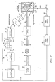
- the substrate 10 is mounted on a base 12 within a reaction chamber.
- Substrate 10 includes an upper chromium layer 14 superposed on a copper layer 16 which, in turn, is coated with a second chromium layer 18 on its other side.
- a reactive gas which, in this case, is chlorine; and a thin layer of chromium chloride forms on the exposed surface of chromium layer 14.
- An excimer laser 20 directs pulses of an etching laser beam 22 upon a region 24 of the substrate.
- Laser wavelengths of 193 nm, 248 nm, 308 nm and 351 nm are suitable for etching metal chlorides.
- the chromium chloride layer irradiated by the laser beam is vaporized and driven off, exposing a fresh chromium surface in region 24, which again reacts with the chlorine gas to form a chromium chloride layer.
- the next laser pulse then removes the newly formed chromium chloride layer. This process of forming a thin layer of chromium chloride on region 24 and removing the layer with an excimer laser pulse continues until all of the chromium layer in region 24 is consumed to expose copper layer 16.
- the chlorine gas then reacts with the exposed copper in region 24 to form a thin layer of copper chloride.
- the next excimer laser pulse vaporizes the thin copper chloride layer in region 24 and ejects the copper chloride from region 24 through a detection zone 26 spaced 1 to 2 cm from region 24 in a direction normal to region 24. If detection zone 26 is spaced at a distance from substrate 10 which is significantly greater than 1 cm, the possibility that the copper chloride will condense on cold surface increases. One can anticipate that detection at greater distances will be less sensitive.
- a tunable dye laser 28 is used to direct pulses of a probe beam 30 through region 26.
- the wavelength of beam 30 is 433.3 nm, selected to match the spectroscopic characteristics of copper chloride. Light of this wavelength is absorbed by copper chloride in its gas phase, inducing the copper chloride to fluoresce light 32 at a wavelength of 441.2 nm which is unique to copper chloride.
- the pulsing of dye laser 28 is timed to coincide with the arrival in zone 26 of the vaporized reaction product ejected from region 24.
- dye laser 28 is timed to pulse 12 microseconds after the pulsing of excimer laser 20.
- the copper chloride in gas phase entering zone 26 will absorb the 433.3 nm light from probe beam 30 and fluoresce light 32 at 441.2 nm. Some of the copper chloride molecules will remain in the gas phase from one etch laser pulse to the next, which increases the sensitivity of the technique.
- the 441.2 nm light is directed by a collecting lens 34 to a monochromator 38 set to pass light of 441.2 nm wavelength.
- Monochromator 38 has an aperture 40 receiving the 441.2 nm light, directing it at 42 to grating 44 from which the light 46 is directed to photomultiplier tube 48.
- the output from photomultiplier tube 48 is used to drive a meter or recorder 50 which provides an indication that light of 441.2 nm wavelength has been received and, hence, that the end point in the etching of substrate 10 has been reached.
- the detection of the end point can be used to terminate the etching process.
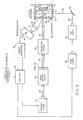
- the embodiment shown in fig. 2 has this capability.
- the excimer laser 20 is pulsed by a pulse generator 51 which may, for example, be a programmable pulse generator of the type manufactured by Tektronix.
- Pulse generator 51 is programmed to generate pulses of a given voltage and frequency. Since the strength of the external signal needed to trigger an excimer laser varies from one laser manufacturer to another, the voltage of the pulses generated should be matched to the requirements for triggering the excimer laser used.
- excimer laser 20 may be pulsed at a rate as low as 10 pulses per second, for most applications a laser repetition rate as high as commercially available lasers will allow, which at present is 500 Hz, is used.
- the pulse width of the excimer laser should be in the range of 10 nanoseconds to 650 microseconds, and the intensity should be in the range of 1 to 3 MW/sq. cm. More recently, however, intensities in the range of 7 to 10 MW/sq. cm have been used successfully.
- the laser radiation beam 22 emitted by laser 20 is passed through beam shaping optics 58 and a mask 60 which determines the pattern to be etched.
- the patterned laser beam 62 is collected by projection optics 64, and a focused image 66 of the mask is projected through the front window 68 of the reaction chamber 70 into which chlorine gas has been introduced.
- the beam impinges upon substrate 10 to etch a region of the substrate corresponding to the pattern.
- Substrate 10 which again is a chromium-copper-chromium substrate having a chromium layer 14, a copper layer 16 and a chromium layer 18, is mounted on base 12.
- Reaction chamber 70 has side walls 72 and 74, and a side window 76 is provided in side wall 72.
- Dye laser 28 is pulsed to direct a probe beam 30 of 433.3 nm reflected by mirror 82 into reaction chamber 70 through side window 76 and into zone 26.
- Pulse generator 51 pulses dye laser 28 after a delay. This delay, which in the case of zone 26 set at 1 to 2 cm from substrate 10 is 12 microseconds, is provided in part by a delay generator 78 pulsed by pulse generator 51.
- the output 79 from delay generator 78 pulses a pump laser 80 after a predetermined delay; and pump laser 80, in turn, triggers dye laser 28.
- the 12 microsecond delay is the sum of the delay provided by delay generator 78 and the inherent delay in pump laser 80.
- the 433.3 nm probe beam from dye laser 28 is strongly absorbed by the ejected copper chloride gas in zone 26 which then reemits, by fluorescence, light at 441.2 nm.
- the 441.2 nm light 32 is collected by collecting lens 34 and passed through monochromator 38, which is set to pass light of the 441.2 nm wavelength, to photomultiplier tube 48.
- the output voltage of photomultiplier tube 48 rises and is fed to the input terminal 83 of a boxcar integrator 84 which integrates the signal over a period corresponding to two to three fluorescent lifetimes of the light fluorescing at 441.2 nm. Since this fluorescent lifetime for copper chloride is 0.6 microseconds, the integration period of boxcar integrator is set at 1.2 - 1.8 microseconds.
- the integrator is reset by a pulse on line 86 from delay generator 78 applied to terminal 88, which pulse coincides with the pulse on line 79 to pump laser 80.
- the integrated signal is negative and reduces the voltage output across output terminals 85a and 85b of the integrator.
- This output voltage of integrator 84 serves as a voltage source for a relay circuit including relay 55.
- the voltage on the output terminals of integrator 84 is large enough to energize relay 55 when a manual start switch 53 is closed bridging contacts 54a and 54b. This causes the relay to close power switch 52 of pulse generator 51 to turn on the pulse generator and to close a holding switch 56 to maintain the energization of relay 55.
- the photomultiplier tube output signal being integrated becomes large enough to pull down the voltage across output terminals 85a and 85b below the holding voltage of relay 55, relay 55 opens holding switch 56 and power switch 52 to shut off the pulse generator. With pulse generator 51 shut down, the pulsing of excimer laser 20 ceases; and the etching process is terminated.
- the magnitude of the signal required to release the relay can be adjusted to control the amount of chromium remaining in region 24. It is thus possible to stop the excimer laser immediately after the first copper chloride is detected, when some chromium is still present in region 24, or to stop it later after additional copper and the remaining chromium have been etched and the concentration of copper chloride in the gas phase has increased. Such an increase in copper chloride concentration will cause more intense fluorescence of light at 441.2 nm and a larger signal output from photomultiplier tube 48.
- the chromium chloride has not been observed to absorb at 433.3 nm. Therefore, there is no fluorescence emitted by chromium chloride in the gas phase.
- the laser induced fluorescence technique has a demonstrated sensitivity of 10 nm units of copper. There is, thus, very little attack on copper layer 16 before the "stop" signal is generated.
- a mechanical relay is used to control the shutting down of pulse generator 51. While the speed of operation of the relay is adequate for the case of an excimer laser being pulsed at a relatively low rate, such as 10 times per second, in cases requiring a high pulsing rate it will be necessary to employ a faster acting semiconductor circuit analog of the relay circuit to shut down pulse generator 51.
- a computer 94 having a keyboard 96, to automate many of the functions needed to etch the substrate 10 including controlling the firing of excimer laser 20 and controlling the end point detection system.
- the computer incorporates the functions of pulse generator 51, delay generator 78 and the relay circuit of Fig. 2.
- the system of Fig. 3 is otherwise identical to the system shown in Fig. 2.
- computer 94 controls excimer laser 20 in one of two ways.
- Most current excimer lasers have BNC ports which allow the excimer laser to be triggered by an external signal.
- a pulse generating card is provided in the computer; and the computer is programmed to send pulses of appropriate voltage and frequency to the laser.
- a few currently available excimer lasers, and all excimer lasers planned as industrial tools, have a microprocessor built into the laser itself.
- the laser based microprocessor controls many of the functions of the laser including setting the repetition rate and firing the laser pulses and is designed to interface with an external computer.
- computer 94 is programmed to interface with and set the repetition rate for the laser based microprocessor and to order the laser microprocessor to fire the laser.
- Dye lasers which are computer controlled are now the rule rather than the exception.
- the programs necessary to run dye laser 28 are adapted to the specific requirements of computer 94.
- the output voltage from boxcar integrator 84 can either be read directly by computer 94 after appropriate calibration of its data acquisition card or by first sending the output of boxcar integrator 84 through a programmable voltmeter.
- computer 94 could, in addition to controlling excimer laser 20, dye laser 28, and the end point detection system, control parts changing and handling apparatus and control the atmosphere within reaction cell 70.
- An operator uses computer 94 to set the repetition rate and output energy at which excimer laser 20 will operate. The operator then initiates the main computer program which controls all aspects of the etching. Computer 94 waits for a signal from the parts handling system that a substrate is in place and ready to be etched before proceeding with laser etching and end point detection.
- the operator initiates the laser etching and end point detection systems.
- computer 94 checks that dye laser 28 is running and producing light at the proper wavelength.
- the wavelength is set at 433.3 nm for detection of copper chloride.
- Whatever corrective action that is necessary is directed by the computer including turning pump laser 80 and dye laser 28 on, tuning dye laser 28 to the proper wavelength, and timing the pulsing of dye laser 28 to fire after a delay following the time of firing of the excimer laser to maximize the intensity of the light fluoresced by copper chloride in gas phase.
- the delay is selected so that the probe beam 30 from dye laser 28 will pass through a zone 26 spaced from substrate 10 when the reaction product ejected from substrate 10 after vaporization by the excimer laser beam has reached zone 26. As explained above, a delay of 12 microseconds is appropriate for a zone 26 spaced 1 to 2 cm from substrate 10. Dye laser 28 may be left running, or may be turned off, while substrates are being removed and placed in reaction chamber 70.
- the system After the computer starts firing excimer laser 20, the system operates as explained above in connection with Fig. 2.
- the voltage appearing at the output of boxcar integrator 84 which is reset by the computer at about the time dye laser 28 is fired, is read by computer 94 and compared to a stored voltage value.
- a stored voltage value At first, when only chromium is being etched and chromium chloride is being ejected from substrate 10, there is no fluorescence at 441.2 nm and the output of boxcar integrator 84 remains below the stored voltage value in computer 94.
- the stored voltage value is determined experimentally and is the voltage at which gas phase copper chloride is first detected.
- the underlying copper begins to be etched and copper chloride is ejected into the atmosphere above the substrate surface.
- the copper chloride in gas phase strongly absorbs the 433.3 nm dye laser light and reemits, by fluorescence, light at 441.2 nm.
- the output voltage of boxcar integrator 84 rises and exceeds the voltage value stored in computer 94.
- the computer either immediately stops excimer laser 20 from pulsing or pulses excimer laser 20 for a set number of additional pulses to remove all of the residual chromium from region 24 before stopping the laser.
- reaction products which may be formed by a reactive gas when an overlying layer is etched through to expose an underlying layer in the above described etching process, may be detected as well by tuning the dye laser to an appropriate excitation wavelength and by selecting a monochrometer tuned to pass the luminescent light emitted by the reaction product.
- the following table contains an exemplary list of such reaction products along with the wavelength of the excitation probe beam required and the wavelength of the luminescent light emitted:
- the pulsing of dye laser 28 is keyed to occur at a fixed delay after the pulsing of the excimer laser.
- the pulsing of the dye laser need not be synchronized to the pulsing of the excimer laser: it is only necessary that at least one of the dye laser pulses coincide with the time of arrival of ejected reaction product in zone 26.
- probe beam source it is possible to use light sources other than dye lasers as the probe beam source.
- properly tuned resonance lamps could be used.
- the sensitivity will probably be too low and slow for most purposes.
- narrow band optical filters could be used.
Landscapes
- Chemical & Material Sciences (AREA)
- Engineering & Computer Science (AREA)
- Materials Engineering (AREA)
- Mechanical Engineering (AREA)
- Metallurgy (AREA)
- Organic Chemistry (AREA)
- Drying Of Semiconductors (AREA)
- ing And Chemical Polishing (AREA)
- Investigating, Analyzing Materials By Fluorescence Or Luminescence (AREA)
Applications Claiming Priority (2)
| Application Number | Priority Date | Filing Date | Title |
|---|---|---|---|
| US06/924,519 US4687539A (en) | 1986-10-29 | 1986-10-29 | End point detection and control of laser induced dry chemical etching |
| US924519 | 1997-09-05 |
Publications (2)
| Publication Number | Publication Date |
|---|---|
| EP0265764A1 true EP0265764A1 (de) | 1988-05-04 |
| EP0265764B1 EP0265764B1 (de) | 1991-01-16 |
Family
ID=25450312
Family Applications (1)
| Application Number | Title | Priority Date | Filing Date |
|---|---|---|---|
| EP87114911A Expired EP0265764B1 (de) | 1986-10-29 | 1987-10-13 | Verfahren und Vorrichtung für durch Bestrahlung induziertes chemisches Trockenätzen |
Country Status (4)
| Country | Link |
|---|---|
| US (1) | US4687539A (de) |
| EP (1) | EP0265764B1 (de) |
| JP (1) | JPS63116431A (de) |
| DE (1) | DE3767436D1 (de) |
Cited By (2)
| Publication number | Priority date | Publication date | Assignee | Title |
|---|---|---|---|---|
| DE3935189A1 (de) * | 1989-10-23 | 1991-05-08 | Leybold Ag | Verfahren und vorrichtung zur behandlung von werkstuecken durch reaktives ionenaetzen |
| EP0454604A3 (en) * | 1990-03-30 | 1992-10-21 | International Business Machines Corporation | Laser ablation for plasma etching endpoint detection |
Families Citing this family (34)
| Publication number | Priority date | Publication date | Assignee | Title |
|---|---|---|---|---|
| US5064681A (en) * | 1986-08-21 | 1991-11-12 | International Business Machines Corporation | Selective deposition process for physical vapor deposition |
| US4960495A (en) * | 1987-06-26 | 1990-10-02 | Mikakto Precision Engineering Research Institute Co., Ltd. | Process for precise processing of workpiece using free radicals |
| US5531857A (en) * | 1988-07-08 | 1996-07-02 | Cauldron Limited Partnership | Removal of surface contaminants by irradiation from a high energy source |
| US5821175A (en) * | 1988-07-08 | 1998-10-13 | Cauldron Limited Partnership | Removal of surface contaminants by irradiation using various methods to achieve desired inert gas flow over treated surface |
| US5099557A (en) * | 1988-07-08 | 1992-03-31 | Engelsberg Audrey C | Removal of surface contaminants by irradiation from a high-energy source |
| DE68919328T2 (de) * | 1988-10-28 | 1995-05-24 | Ibm | Ultraviolette Laserablation und Ätzen von organischen Feststoffen. |
| US4902631A (en) * | 1988-10-28 | 1990-02-20 | At&T Bell Laboratories | Monitoring the fabrication of semiconductor devices by photon induced electron emission |
| US4940508A (en) * | 1989-06-26 | 1990-07-10 | Digital Equipment Corporation | Apparatus and method for forming die sites in a high density electrical interconnecting structure |
| US4980018A (en) * | 1989-11-14 | 1990-12-25 | Intel Corporation | Plasma etching process for refractory metal vias |
| US5318662A (en) * | 1989-12-20 | 1994-06-07 | Texas Instruments Incorporated | Copper etch process using halides |
| JP3128231B2 (ja) * | 1990-07-24 | 2001-01-29 | ソニー株式会社 | 銅系材料のパターニング方法 |
| US5362356A (en) * | 1990-12-20 | 1994-11-08 | Lsi Logic Corporation | Plasma etching process control |
| JPH04225525A (ja) * | 1990-12-27 | 1992-08-14 | Sony Corp | ドライエッチング方法 |
| EP0511448A1 (de) * | 1991-04-30 | 1992-11-04 | International Business Machines Corporation | Verfahren und Vorrichtung zur in-situ und in-Linie Überwachung eines Graben-Herstellungsverfahrens |
| US5245794A (en) * | 1992-04-09 | 1993-09-21 | Advanced Micro Devices, Inc. | Audio end point detector for chemical-mechanical polishing and method therefor |
| TW260857B (de) * | 1993-03-04 | 1995-10-21 | Tokyo Electron Co Ltd | |
| US5814156A (en) * | 1993-09-08 | 1998-09-29 | Uvtech Systems Inc. | Photoreactive surface cleaning |
| AU7682594A (en) * | 1993-09-08 | 1995-03-27 | Uvtech Systems, Inc. | Surface processing |
| DE19725520A1 (de) * | 1996-07-01 | 1998-01-08 | Emtec Magnetics Gmbh | Verfahren und Anordnung zur laser-induzierten Spektralanalyse |
| US6106683A (en) * | 1997-06-23 | 2000-08-22 | Toyo Technologies Inc. | Grazing angle plasma polisher (GAPP) |
| US5961859A (en) * | 1997-10-23 | 1999-10-05 | Trw Inc. | Method and apparatus for monitoring laser weld quality via plasma size measurements |
| US6060685A (en) * | 1997-10-23 | 2000-05-09 | Trw Inc. | Method for monitoring laser weld quality via plasma light intensity measurements |
| WO2001068271A1 (en) * | 2000-03-15 | 2001-09-20 | Tufts University | Controlling surface chemistry on solid substrates |
| DE10210518A1 (de) * | 2002-03-09 | 2003-10-02 | Mtu Aero Engines Gmbh | Verfahren zur Entschichtung von Triebwerksbauteilen und Vorrichtung zur Durchführung des Verfahrens |
| US6979579B1 (en) * | 2004-03-30 | 2005-12-27 | Lam Research Corporation | Methods and apparatus for inspecting contact openings in a plasma processing system |
| CN101891680B (zh) | 2004-06-24 | 2014-10-29 | 沃泰克斯药物股份有限公司 | Atp-结合弹夹转运蛋白的调控剂 |
| US8354427B2 (en) | 2004-06-24 | 2013-01-15 | Vertex Pharmaceutical Incorporated | Modulators of ATP-binding cassette transporters |
| DK3219705T3 (da) | 2005-12-28 | 2020-04-14 | Vertex Pharma | Farmaceutiske sammensætninger af den amorfe form af n-[2,4-bis(1,1-dimethylethyl)-5-hydroxyphenyl]-1,4-dihydro-4-oxoquinolin-3-carboxamid |
| GB2441582A (en) * | 2006-09-01 | 2008-03-12 | Gencoa Ltd | Process monitoring and control |
| US8802700B2 (en) | 2010-12-10 | 2014-08-12 | Vertex Pharmaceuticals Incorporated | Modulators of ATP-Binding Cassette transporters |
| US8802545B2 (en) * | 2011-03-14 | 2014-08-12 | Plasma-Therm Llc | Method and apparatus for plasma dicing a semi-conductor wafer |
| JP5902540B2 (ja) * | 2012-04-02 | 2016-04-13 | 株式会社ディスコ | レーザー加工方法およびレーザー加工装置 |
| CN107250113B (zh) | 2014-10-07 | 2019-03-29 | 弗特克斯药品有限公司 | 囊性纤维化跨膜传导调节蛋白的调节剂的共晶 |
| CN117270317B (zh) * | 2023-11-20 | 2024-02-09 | 深圳市龙图光罩股份有限公司 | 图形辅助的干法刻蚀装置及方法 |
Citations (8)
| Publication number | Priority date | Publication date | Assignee | Title |
|---|---|---|---|---|
| US4198261A (en) * | 1977-12-05 | 1980-04-15 | Gould Inc. | Method for end point detection during plasma etching |
| US4379022A (en) * | 1979-05-08 | 1983-04-05 | International Business Machines Corporation | Method for maskless chemical machining |
| US4393311A (en) * | 1980-06-13 | 1983-07-12 | Bell Telephone Laboratories, Incorporated | Method and apparatus for surface characterization and process control utilizing radiation from desorbed particles |
| US4394237A (en) * | 1981-07-17 | 1983-07-19 | Bell Telephone Laboratories, Incorporated | Spectroscopic monitoring of gas-solid processes |
| US4398993A (en) * | 1982-06-28 | 1983-08-16 | International Business Machines Corporation | Neutralizing chloride ions in via holes in multilayer printed circuit boards |
| US4490210A (en) * | 1984-01-24 | 1984-12-25 | International Business Machines Corporation | Laser induced dry chemical etching of metals |
| US4490211A (en) * | 1984-01-24 | 1984-12-25 | International Business Machines Corporation | Laser induced chemical etching of metals with excimer lasers |
| EP0186419A2 (de) * | 1984-12-26 | 1986-07-02 | Hitachi, Ltd. | Verfahren zum Trockenätzen oder zur Überzugsherstellung |
Family Cites Families (2)
| Publication number | Priority date | Publication date | Assignee | Title |
|---|---|---|---|---|
| US4377436A (en) * | 1980-05-13 | 1983-03-22 | Bell Telephone Laboratories, Incorporated | Plasma-assisted etch process with endpoint detection |
| JPS6050923A (ja) * | 1983-08-31 | 1985-03-22 | Hitachi Ltd | プラズマ表面処理方法 |
-
1986
- 1986-10-29 US US06/924,519 patent/US4687539A/en not_active Expired - Lifetime
-
1987
- 1987-07-20 JP JP62179272A patent/JPS63116431A/ja active Granted
- 1987-10-13 EP EP87114911A patent/EP0265764B1/de not_active Expired
- 1987-10-13 DE DE8787114911T patent/DE3767436D1/de not_active Expired - Lifetime
Patent Citations (10)
| Publication number | Priority date | Publication date | Assignee | Title |
|---|---|---|---|---|
| US4198261A (en) * | 1977-12-05 | 1980-04-15 | Gould Inc. | Method for end point detection during plasma etching |
| US4379022A (en) * | 1979-05-08 | 1983-04-05 | International Business Machines Corporation | Method for maskless chemical machining |
| US4393311A (en) * | 1980-06-13 | 1983-07-12 | Bell Telephone Laboratories, Incorporated | Method and apparatus for surface characterization and process control utilizing radiation from desorbed particles |
| US4394237A (en) * | 1981-07-17 | 1983-07-19 | Bell Telephone Laboratories, Incorporated | Spectroscopic monitoring of gas-solid processes |
| US4398993A (en) * | 1982-06-28 | 1983-08-16 | International Business Machines Corporation | Neutralizing chloride ions in via holes in multilayer printed circuit boards |
| US4490210A (en) * | 1984-01-24 | 1984-12-25 | International Business Machines Corporation | Laser induced dry chemical etching of metals |
| US4490211A (en) * | 1984-01-24 | 1984-12-25 | International Business Machines Corporation | Laser induced chemical etching of metals with excimer lasers |
| EP0149779A2 (de) * | 1984-01-24 | 1985-07-31 | International Business Machines Corporation | Chemisches Ätzen von Metallen induziert durch Eximer-Lasern |
| EP0150358A2 (de) * | 1984-01-24 | 1985-08-07 | International Business Machines Corporation | Chemisches Ätzen von Metallen induziert durch einen Laser |
| EP0186419A2 (de) * | 1984-12-26 | 1986-07-02 | Hitachi, Ltd. | Verfahren zum Trockenätzen oder zur Überzugsherstellung |
Non-Patent Citations (3)
| Title |
|---|
| Applied Physic Letters, Vol. 45, August 15, 1984 R. WALKUP et al. "Laser Detection of Diatomic Products of Plasma Sputtering and Etching" pages 372-374 * Totality * * |
| PATENT ABSTRACTS OF JAPAN, Unexamined Applications, C Field, Vol. 10, No. 194, July 8, 1986 The Patent Office Japanese Government page 139 C 358 * Kokai-No. 61-37 981 (Toshiba Corp.) * * |
| PATENT ABSTRACTS OF JAPAN, Unexamined Applications, C Field, Vol. 11, No. 3, January 7, 1987 The Patent Office Japanese Government page 12 C 395 * Kokai-No. 61-179 884 (Mitsubishi Electric Corp.) 12.8.1986 * * |
Cited By (2)
| Publication number | Priority date | Publication date | Assignee | Title |
|---|---|---|---|---|
| DE3935189A1 (de) * | 1989-10-23 | 1991-05-08 | Leybold Ag | Verfahren und vorrichtung zur behandlung von werkstuecken durch reaktives ionenaetzen |
| EP0454604A3 (en) * | 1990-03-30 | 1992-10-21 | International Business Machines Corporation | Laser ablation for plasma etching endpoint detection |
Also Published As
| Publication number | Publication date |
|---|---|
| EP0265764B1 (de) | 1991-01-16 |
| JPS63116431A (ja) | 1988-05-20 |
| US4687539A (en) | 1987-08-18 |
| DE3767436D1 (de) | 1991-02-21 |
| JPH0558651B2 (de) | 1993-08-27 |
Similar Documents
| Publication | Publication Date | Title |
|---|---|---|
| EP0265764B1 (de) | Verfahren und Vorrichtung für durch Bestrahlung induziertes chemisches Trockenätzen | |
| US6509960B2 (en) | Method and apparatus employing external light source for endpoint detection | |
| US5683538A (en) | Control of etch selectivity | |
| EP0119455B1 (de) | Ätzverfahren und -gerät | |
| US4152723A (en) | Method of inspecting circuit boards and apparatus therefor | |
| US5465154A (en) | Optical monitoring of growth and etch rate of materials | |
| RU2205384C2 (ru) | Способ и устройство для лазерного анализа диоксинов | |
| JPS642332A (en) | Method and device for testing desired area of workpiece by designating the area | |
| US4902631A (en) | Monitoring the fabrication of semiconductor devices by photon induced electron emission | |
| JP2000292129A (ja) | エッチング深さ測定方法および装置 | |
| US4263089A (en) | Plasma development process controller | |
| US4246060A (en) | Plasma development process controller | |
| JPH0641885B2 (ja) | 気体ビームを用いた超短レーザーパルス測定方法 | |
| JP2005201762A (ja) | リチウム漏洩検出装置およびリチウム漏洩検出方法 | |
| JPS5665973A (en) | Vapor depositing method | |
| JPH07124766A (ja) | エキシマレーザ加工制御方法 | |
| US12158374B2 (en) | Time-resolved OES data collection | |
| KR20030030910A (ko) | 반도체 공정에서의 종점 검출을 위한 안정화된 펄스광구동회로 장치 및 방법 | |
| JPH055301B2 (de) | ||
| JP3388601B2 (ja) | 集束イオンビーム加工の終点検出方法およびそれを用いた加工装置 | |
| JPH0674897A (ja) | 水質検査方法及びその装置 | |
| JPS6285847A (ja) | レ−ザ多段励起直接発光分析方法及び装置 | |
| JPH0618337A (ja) | ガス温度計測方法 | |
| WO1994006151A1 (fr) | Procede de detection concernant une profondeur de gravure | |
| JPH09283497A (ja) | ドライエッチングの終点検出方法 |
Legal Events
| Date | Code | Title | Description |
|---|---|---|---|
| PUAI | Public reference made under article 153(3) epc to a published international application that has entered the european phase |
Free format text: ORIGINAL CODE: 0009012 |
|
| AK | Designated contracting states |
Kind code of ref document: A1 Designated state(s): DE FR GB |
|
| 17P | Request for examination filed |
Effective date: 19880823 |
|
| 17Q | First examination report despatched |
Effective date: 19890925 |
|
| GRAA | (expected) grant |
Free format text: ORIGINAL CODE: 0009210 |
|
| AK | Designated contracting states |
Kind code of ref document: B1 Designated state(s): DE FR GB |
|
| REF | Corresponds to: |
Ref document number: 3767436 Country of ref document: DE Date of ref document: 19910221 |
|
| ET | Fr: translation filed | ||
| PGFP | Annual fee paid to national office [announced via postgrant information from national office to epo] |
Ref country code: GB Payment date: 19910923 Year of fee payment: 5 |
|
| PGFP | Annual fee paid to national office [announced via postgrant information from national office to epo] |
Ref country code: FR Payment date: 19911001 Year of fee payment: 5 |
|
| PGFP | Annual fee paid to national office [announced via postgrant information from national office to epo] |
Ref country code: DE Payment date: 19911102 Year of fee payment: 5 |
|
| PLBE | No opposition filed within time limit |
Free format text: ORIGINAL CODE: 0009261 |
|
| STAA | Information on the status of an ep patent application or granted ep patent |
Free format text: STATUS: NO OPPOSITION FILED WITHIN TIME LIMIT |
|
| 26N | No opposition filed | ||
| PG25 | Lapsed in a contracting state [announced via postgrant information from national office to epo] |
Ref country code: GB Effective date: 19921013 |
|
| GBPC | Gb: european patent ceased through non-payment of renewal fee |
Effective date: 19921013 |
|
| PG25 | Lapsed in a contracting state [announced via postgrant information from national office to epo] |
Ref country code: FR Effective date: 19930630 |
|
| PG25 | Lapsed in a contracting state [announced via postgrant information from national office to epo] |
Ref country code: DE Effective date: 19930701 |
|
| REG | Reference to a national code |
Ref country code: FR Ref legal event code: ST |