EP0266768A1 - Herstellungsverfahren zur Ausbildung eines MOS-Transistors durch Selbstausrichtung der Source/Drain-Gebiete - Google Patents
Herstellungsverfahren zur Ausbildung eines MOS-Transistors durch Selbstausrichtung der Source/Drain-Gebiete Download PDFInfo
- Publication number
- EP0266768A1 EP0266768A1 EP87116309A EP87116309A EP0266768A1 EP 0266768 A1 EP0266768 A1 EP 0266768A1 EP 87116309 A EP87116309 A EP 87116309A EP 87116309 A EP87116309 A EP 87116309A EP 0266768 A1 EP0266768 A1 EP 0266768A1
- Authority
- EP
- European Patent Office
- Prior art keywords
- impurity
- mos transistor
- mask member
- conductivity type
- semiconductor substrate
- Prior art date
- Legal status (The legal status is an assumption and is not a legal conclusion. Google has not performed a legal analysis and makes no representation as to the accuracy of the status listed.)
- Granted
Links
Images






Classifications
-
- H—ELECTRICITY
- H10—SEMICONDUCTOR DEVICES; ELECTRIC SOLID-STATE DEVICES NOT OTHERWISE PROVIDED FOR
- H10D—INORGANIC ELECTRIC SEMICONDUCTOR DEVICES
- H10D30/00—Field-effect transistors [FET]
- H10D30/01—Manufacture or treatment
- H10D30/021—Manufacture or treatment of FETs having insulated gates [IGFET]
- H10D30/0223—Manufacture or treatment of FETs having insulated gates [IGFET] having source and drain regions or source and drain extensions self-aligned to sides of the gate
- H10D30/0227—Manufacture or treatment of FETs having insulated gates [IGFET] having source and drain regions or source and drain extensions self-aligned to sides of the gate having both lightly-doped source and drain extensions and source and drain regions self-aligned to the sides of the gate, e.g. lightly-doped drain [LDD] MOSFET or double-diffused drain [DDD] MOSFET
-
- H—ELECTRICITY
- H10—SEMICONDUCTOR DEVICES; ELECTRIC SOLID-STATE DEVICES NOT OTHERWISE PROVIDED FOR
- H10D—INORGANIC ELECTRIC SEMICONDUCTOR DEVICES
- H10D30/00—Field-effect transistors [FET]
- H10D30/60—Insulated-gate field-effect transistors [IGFET]
- H10D30/601—Insulated-gate field-effect transistors [IGFET] having lightly-doped drain or source extensions, e.g. LDD IGFETs or DDD IGFETs
- H10D30/605—Insulated-gate field-effect transistors [IGFET] having lightly-doped drain or source extensions, e.g. LDD IGFETs or DDD IGFETs having significant overlap between the lightly-doped extensions and the gate electrode
-
- H—ELECTRICITY
- H10—SEMICONDUCTOR DEVICES; ELECTRIC SOLID-STATE DEVICES NOT OTHERWISE PROVIDED FOR
- H10D—INORGANIC ELECTRIC SEMICONDUCTOR DEVICES
- H10D62/00—Semiconductor bodies, or regions thereof, of devices having potential barriers
- H10D62/10—Shapes, relative sizes or dispositions of the regions of the semiconductor bodies; Shapes of the semiconductor bodies
- H10D62/13—Semiconductor regions connected to electrodes carrying current to be rectified, amplified or switched, e.g. source or drain regions
- H10D62/149—Source or drain regions of field-effect devices
- H10D62/151—Source or drain regions of field-effect devices of IGFETs
-
- H—ELECTRICITY
- H10—SEMICONDUCTOR DEVICES; ELECTRIC SOLID-STATE DEVICES NOT OTHERWISE PROVIDED FOR
- H10D—INORGANIC ELECTRIC SEMICONDUCTOR DEVICES
- H10D89/00—Aspects of integrated devices not covered by groups H10D84/00 - H10D88/00
- H10D89/60—Integrated devices comprising arrangements for electrical or thermal protection, e.g. protection circuits against electrostatic discharge [ESD]
- H10D89/601—Integrated devices comprising arrangements for electrical or thermal protection, e.g. protection circuits against electrostatic discharge [ESD] for devices having insulated gate electrodes, e.g. for IGFETs or IGBTs
- H10D89/811—Integrated devices comprising arrangements for electrical or thermal protection, e.g. protection circuits against electrostatic discharge [ESD] for devices having insulated gate electrodes, e.g. for IGFETs or IGBTs using FETs as protective elements
-
- H—ELECTRICITY
- H10—SEMICONDUCTOR DEVICES; ELECTRIC SOLID-STATE DEVICES NOT OTHERWISE PROVIDED FOR
- H10P—GENERIC PROCESSES OR APPARATUS FOR THE MANUFACTURE OR TREATMENT OF DEVICES COVERED BY CLASS H10
- H10P76/00—Manufacture or treatment of masks on semiconductor bodies, e.g. by lithography or photolithography
- H10P76/20—Manufacture or treatment of masks on semiconductor bodies, e.g. by lithography or photolithography of masks comprising organic materials
- H10P76/204—Manufacture or treatment of masks on semiconductor bodies, e.g. by lithography or photolithography of masks comprising organic materials of organic photoresist masks
- H10P76/2041—Photolithographic processes
Definitions
- the present invention relates to a method of manufacturing a semiconductor device, to form a MOS transistor by self-alignment.
- a special circuit for preventing the inner elements from breaking down as a result of an externally applied surge (pulse-like stress) or a DC stress (static high-voltage stress).
- This special circuit will hereinafter be referred to as an input protecting circuit.
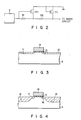
- Fig. 1 shows an example of the structure of a semiconductor integrated circuit wherein an electrical signal passes through lead 1, Au wire 2 electrically connected to lead 1, and A1 pattern 3 electrically connected to wire 2 and formed on semiconductor substrate 5, and reaches inner circuit 41 via input protecting circuit 4.
- reference numeral 6 denotes a semiconductor integrated circuit; and 7, molded resin.
- Circuit 4 comprises resistors R1 and R2 and MOS transistors Tr1 and Tr2.
- a surge entering to pattern 3 is attenuated by resistors R1 and R2 and is absorbed by MOS transistors Tr1 and Tr2.
- a static DC stress is absorbed by MOS transistor Tr2.
- Figs. 3 and 4 are sectional views of conventional MOS transistors Tr1 and Tr2.
- source region 11 and drain region 12 are formed in substrate 5, as are also gate insulating film 13 and gate electrode 14.
- Fig. 4 shows a MOS transistor in which shallow regions 17 and 18 having an impurity concentration lower than that of source region 15 and drain region 16 are formed between regions 15 and 16 and electrode 14.
- the MOS transistor shown in Fig. 4 is known as an LDD (lightly doped drain) transistor and has a structure which is advantageous as regards the micropatterning thereof.
- MOS transistors Tr1 and Tr2 are shown in Figs. 5A and 5B.
- the source and drain regions of a MOS transistor of an input protecting circuit are formed by self-alignment, together with those of a MOS transistor of an inner circuit. That is, a thermal oxide film 13 and polysilicon 14 are formed on the surface of substrate 5 and then patterned, thereby forming gate oxide film 13 and gate electrode 14.
- impurity 21 of a conductivity type different from that of substrate 5 is ion-implanted in the prospective source and drain region formation areas (Fig. 5A).
- source region 11 and drain region 12 are formed by thermal diffusion (Fig. 5B).
- depth xj of source and drain regions of a MOS transistor is generally shallow and the impurity concentration of them is generally high (Fig. 6).
- radius of curvature R of a junction side surface is reduced, which leads to an increase in the electric field in the depletion layer at the junction side surface, thereby degrading the junction breakdown withstand voltage.
- the present invention is characterized in that an impurity of a conductivity type opposite to that of a semiconductor substrate is doped, through a mask, in the prospective source and drain region formation areas of a MOS transistor of an input protecting circuit, the source and drain regions are formed by mask alignment, an insulating film and a conductive film are sequentially formed after the mask member is removed, the desired patterns are etched on the insulating and conductive films, to form a gate insulating film and a gate electrode of a MOS transistor of an inner circuit and those of the MOS transistor of the input protecting circuit, an impurity of a conductivity type opposite to that of the semiconductor substrate is doped in at least the prospective source and drain region formation areas of the MOS transistor of the inner circuit, using the gate insulating film and the gate electrode as masks, thereby forming, by self-alignment, at least the source and drain regions of the MOS transistor of the inner circuit.
- the source and drain regions of the MOS transistor of the input protecting circuit are formed by mask alignment, the impurity concentration of the source or drain region is increased to reduce the diffusion resistance, thereby increasing the junction breakdown power generated by a drain current.
- the electric field of the junction curved surface portion is reduced, thereby improving the junction breakdown withstand characteristics.
- the junction breakdown power caused by the drain current is increased. This happens because the junction breakdown power of an LDD transistor having a structure in which the diffusion layer resistances of the source and drain regions of the MOS transistor are high is lower than that of the MOS transistor with a low diffusion layer resistance.
- both the source and drain regions of the MOS transistor are formed to have a low resistance, and the radii of curvature at the junction curved surface portions of the source and drain regions of the MOS transistor are increased.
- the effect of the present invention can also be achieved either by forming the source and drain regions of the MOS transistor to have a low resistance or by increasing the radii of curvature at the junction curved surface portion s thereof.
- the present invention is characterized in that source and drain regions of a MOS transistor of an input protecting circuit of a semiconductor integrated circuit having an input protecting circuit and an inner circuit on a single semiconductor substrate are formed by doping an impurity in the prospective source and drain region formation areas by mask alignment.
- the source and drain regions of the MOS transistor can be formed simultaneously with the formation of well regions during the photolithographic step for forming an n-type well region and a p-type well region of the MOS transistor, thereby reducing the number of manufacturing steps.
- the source and drain regions of the MOS transistor are formed simultaneously with the formation of the well regions of the CMOS transistor, the radii of curvature at the junction curved surface portions of the source and drain regions of the MOS transistor can be increased.
- the source and drain regions of the MOS transistor can be formed by implanting the impurity for depleting the source and drain regions of the MOS transistor during the photolithographic step for implanting the impurity to deplete the MOS capacitor, thereby reducing the number of manufacturing steps.
- the diffusion layers of the source and drain regions can be formed so as to have a low resistance.
- the impurity concentration of the source and drain regions will be lower than that of a depletion region.
- the diffusion resistance of the source and drain regions of the MOS transistor tends to be higher than a specific resistance of the depletion region.
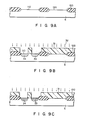
- p-type semiconductor substrate 5 is selectively oxidized in an H2O atmosphere at a temperature of 1,000°C, to selectively form 1- ⁇ m thick field oxide film 100. Thereafter, element region 110 of an input protecting circuit and element region 120 of an inner circuit are formed (Fig. 7A).
- photoresist film 31 is coated over the entire top surface of the substrate 5 and is then patterned to expose only those portions of substrate 5 which correspond respectively to the prospective source and drain region formation areas of the MOS transistor of the input protecting circuit. Then, using patterned film 31 as a mask, n-type ions 32- for instance, phosphorus (P) ions- are ion-implanted, at 100 keV, in the prospective source and drain region formation areas. As a result, source region 33 and drain region 34 of the MOS transistor of the input protecting circuit are formed (Fig. 7B).
- a conductive polysilico n film doped with a p-type impurity having a concentration of about 1019 to 1021 cm ⁇ 3 is formed thereon by use of the LPCVD method.
- Film 13 and the conductive polysilicon film are patterned so as to form gate electrode 20 of the MOS transistor of the input protecting circuit and gate electrode 21 of the MOS transistor of the inner circuit.
- the prospective source and drain region formation areas of the MOS transistor of the inner circuit are formed (Fig. 7C).
- regions 33 and 34 of the MOS transistor of the input protecting circuit are implanted in regions 33 and 34 of the MOS transistor of the input protecting circuit formed in the step shown in Fig. 7B. That is, As ions 35 are implanted in regions 33 and 34 of the MOS transistor of the input protecting circuit, in addition to the phosphorus (P) ions which are implanted therein in the step shown in Fig. 7B. Therefore, regions 33 and 34 of the MOS transistor of the input protecting circuit contain conductive impurities at a high concentration. In addition, since regions 33 and 34 of the MOS transistor of the input protecting circuit are formed by implanting phosphorus (P) ions therein, both regions are therefore deep.
- Figs. 8A and 8B respectively show partial sections of the MOS transistor of the input protecting circuit and that of the inner circuit formed in the steps shown in Figs. 7A to 7D.
- the impurity concentration of the source or drain region of the MOS transistor of the input protecting circuit is N1
- the curvature of the junction side surface thereof is r1
- the width in a transverse direction thereof is y1
- the impurity concentration of the source or drain region of the MOS transistor of the inner circuit is N2
- the curvature of the junction side surface thereof is r2
- the width in a transverse direction thereof is y2.
- Figs. 9A to 9C are sectional views of manufacturing steps showing another embodiment of a method of manufacturing a semiconductor device according to the present invention. This embodiment of the present invention will now be described below.
- p-type semiconductor substrate 5 is oxidized in an H2O atmosphere at a temperature of 1,000°C, to selectively form 1- ⁇ m thick field oxide film 100. Thereafter, element region 110 of an input protecting circuit and element region 120 of an inner circuit are formed therein (Fig. 9A).
- photoresist film 31 is coated over the entire top surface of film 100 and is then patterned to expose those portions of substrate 5 which correspond respectively to the prospective source and drain region formation areas of the MOS transistor of region 110 of the input protecting circuit. Then, using patterned film 31 as a mask, n-type ions 32- for instance, phosphorus (P) ions- are implanted, at 100 keV, in the prospective source and drain region formation areas. As a result, source region 33 and drain region 34 of the MOS transistor of the input protecting circuit are formed (Fig. 9B).
- the MOS transistor of the input protecting circuit and that of the inner circuit are formed in the same manufacturing steps as those shown in Figs. 7C to 7D.
- the number of ion implantation cycles performed when the source and drain regions of the MOS transistor of the input protecting circuit are formed by mask alignment is not limited to two, but may be a plurality of times more than two.
- Fig. 10 shows a third embodiment of the present invention.
- only one of the source and drain regions of a MOS transistor of an input protecting circuit- for example, source region 33- is formed by mask alignment, using photoresist film 31 as a mask.
- Fig. 11 shows a fourth embodiment of the present invention.
- the source and drain regions of a MOS transistor of an input protecting circuit are both formed by mask alignment of a photoresist film.
- the type of ions implanted in the source region of the MOS transistor differs from that implanted in the drain region thereof. Therefore, since different types of ions are respectively implanted in the source and drain regions of the MOS transistor, the source and drain regions are structurally unbalanced.
- the present invention is not limited to the above embodiments.
- the source and drain regions of the MOS transistor of the input protecting circuit are formed by mask alignment, the gate electrodes of the MOS transistor of the input protecting circuit and that of the inner circuit are then formed, and ions are implanted in the source and drain regions of the MOS transistor of the input protecting circuit and the prospective source and drain region formation areas of the MOS transistor of the inner circuit, using the gate electrodes as masks.
- the source and drain regions of the MOS transistor of the input protecting circuit may be coated with a photoresist film, so as to prevent ion implantation.
- the source and drain regions of the MOS transistor of the input protecting circuit can be formed not by ion implantation but, for example, by diffusion of an impurity.
- a silicon nitride film may be used as a mask against impurity diffusion, and phosphorus ions may be thermally diffused from phosphorus glass containing an impurity of high concentration.
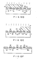
- An inner circuit in this embodiment is formed by a CMOS transistor.
- Photoresist film 31 is coated on p-type semiconductor substrate 5 and is patterned to expose prospective source and drain region formation areas of a MOS transistor of an input protecting circuit and a prospective well region formation area of a CMOS transistor of an inner circuit.
- Phosphorus (P) ions are implanted in these areas using photoresist film 31 as a mask at an acceleration voltage of 130 keV and a dose of 1 ⁇ 10 ⁇ 13 cm ⁇ 2.
- the ion-implanted phosphorus ions are thermally diffused in N2 gas atmosphere at 1,000°C for 2 hours to form source and drain regions 33 and 34 of the MOS transistor of the input protecting circuit and n-type well region 200 of the CMOS transistor of the inner circuit (Fig. 12A).
- substrate 5 is selectively oxidized in H2O atmosphere at 1,000°C to form 1- ⁇ m thick field oxide film 100 (Fig. 12B).
- a 200- ⁇ thick silicon oxide film as a gate oxide of MOS transistor is partially formed on the surface of the P type substrate 5 in HCl gas at 900°C.
- a 4,000- ⁇ thick conductive polysilicon film doped with a n-type impurity of 1019 to 1021 cm ⁇ 3, is formed by LPCVD.
- the silicon o xide and conductive polysilicon films are patterned to form gate oxide film 13 and gate electrode 20 of the MOS transistor of the input protecting circuit and gate oxide films 14a and 14b and gate electrodes 21a and 21b of the CMOS transistor of the inner circuit (Fig. 12C).
- Photoresist film 32 having an opening corresponding to n-type well region 200 of the CMOS transistor is used as a mask to form a p-channel MOS transistor of the CMOS transistor of the inner circuit, and boron ions are implanted through the opening at an acceleration voltage of 100 keV, thereby forming source and drain regions 11a and 12a of the p-channel MOS transistor (Fig. 12D).
- photoresist film 33 masking only the p-channel MOS transistor of the CMOS transistor of the inner circuit is patterned, and arsenic (As) ions are implanted in source and drain regions 33 and 34 of the MOS transistor of the input protecting circuit and the prospective source and drain region formation areas of the n-channel MOS transistor of the inner circuit at an acceleration voltage of 60 keV.
- source and drain regions 11b and 12b of the n-channel MOS transistor of the inner circuit are formed (Fig. 12E).
- Phosphorus may be ion-implanted in place of arsenic.
- photoresist film 33 is eliminated to form the MOS transistor of the input protecting circuit and the CMOS transistor of the inner circuit by carrying out thermal annealing.
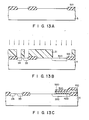
- a fifth embodiment of the present invention will be described with reference to Figs. 13A to 13E.
- This embodiment exemplifies a dynamic memory cell structure as the inner circuit.
- N-type substrate 5 is selectively oxidized in H2O atmosphere at 1,000°C to form 1- ⁇ m thick field oxide film 100.
- prospective input protecting and inner circuit formation areas are defined on substrate 5 (Fig. 13A).
- Photoresist film 31 is coated on the entire surface of substrate 5 including field oxide film 100. Photoresist film 31 is patterned to expose prospective source and drain region formation areas of a MOS transistor of the input protecting circuit and a prospective depletion region formation area of a dynamic memory cell of the inner circuit. Phosphorus (P) ions or Arsenic (As) ions are implanted in the prospective source and drain region formation areas and the prospective depletion region formation area by using photoresist film 31 as a mask at an acceleration voltage of 80 keV and a dose of 1 ⁇ 1014 cm ⁇ 2. As a result, source and drain regions 33 and 34 of the MOS transistor of the input protecting circuit and depletion region 300 of the dynamic memory cells of the inner circuit are formed by thermal annealing after photoresist 31 is removed (Fig. 13B).
- the surface of substrate 5 is thermally oxidized to form a 100- ⁇ thick oxide film thereon, and a polysilicon layer is formed thereon by CVD method and phosphorus (P) is diffused from Pocl 3 gas doping system.
- the oxide film and the polysilicon layer are patterned and are left on a part of depletion region 300 of the dynamic memory cell.
- capacitor insulating film 400 and plate electrode 500 are formed.
- an interlayer insulating film 550 is selectively formed and fully covers the plate electrode (Fig. 13C).
- Substrate 5 is oxidized in HCl atmosphere at 900°C to form a 200- ⁇ thick oxide film.
- a polysilic on layer having a thickness of 4,000 ⁇ is deposited by CVD to cover the entire surface.
- the oxide film and the polysilicon layer are sequentially patterned to form gate insulating film 13 and gate electrode 20 of the MOS transistor of the input protecting circuit and gate insulating film 13 and gate electrode 21 of the inner circuit.
- Arsenic (As) ions are then implanted in the entire surface at an acceleration voltage of 60 keV to form source and drain regions 11 and 12 of the dynamic memory cell.
- Oxide film 600 is formed by CVD to cover the entire surface.
- Contact holes 700 and 800 are formed for source and drain regions 33 and 34 of the MOS transistor of the input protecting circuit and contact holes 900 and 1000 are formed for source and drain regions 11 and 12 of the dynamic memory cell of the inner circuit (Fig. 13E).
Landscapes
- Metal-Oxide And Bipolar Metal-Oxide Semiconductor Integrated Circuits (AREA)
- Semiconductor Memories (AREA)
- Insulated Gate Type Field-Effect Transistor (AREA)
Applications Claiming Priority (2)
| Application Number | Priority Date | Filing Date | Title |
|---|---|---|---|
| JP265022/86 | 1986-11-07 | ||
| JP61265022A JPS63119574A (ja) | 1986-11-07 | 1986-11-07 | 半導体装置の製造方法 |
Publications (2)
| Publication Number | Publication Date |
|---|---|
| EP0266768A1 true EP0266768A1 (de) | 1988-05-11 |
| EP0266768B1 EP0266768B1 (de) | 1994-03-16 |
Family
ID=17411492
Family Applications (1)
| Application Number | Title | Priority Date | Filing Date |
|---|---|---|---|
| EP87116309A Expired - Lifetime EP0266768B1 (de) | 1986-11-07 | 1987-11-05 | Herstellungsverfahren zur Ausbildung eines MOS-Transistors durch Selbstausrichtung der Source/Drain-Gebiete |
Country Status (5)
| Country | Link |
|---|---|
| US (1) | US4950617A (de) |
| EP (1) | EP0266768B1 (de) |
| JP (1) | JPS63119574A (de) |
| KR (1) | KR910005763B1 (de) |
| DE (1) | DE3789350T2 (de) |
Cited By (4)
| Publication number | Priority date | Publication date | Assignee | Title |
|---|---|---|---|---|
| DE4223313A1 (de) * | 1991-07-16 | 1993-01-21 | Mitsubishi Electric Corp | Halbleitervorrichtung und verfahren zu deren herstellung |
| EP0666597A1 (de) * | 1994-01-28 | 1995-08-09 | STMicroelectronics S.A. | Verfahren zur Herstellung eines bipolaren Transistors für den Schutz einer integrierten Schaltung gegen elektrostatische Entladungen |
| EP0675543A3 (de) * | 1994-03-31 | 1996-10-16 | Seiko Instr Inc | Halbleiterbauelement mit einem Schutzmittel und Herstellungsverfahren. |
| EP1223620A3 (de) * | 2001-01-12 | 2003-08-27 | Chartered Semiconductor Manufacturing Pte Ltd. | Elektrostatische Entladung Schutzstruktur |
Families Citing this family (22)
| Publication number | Priority date | Publication date | Assignee | Title |
|---|---|---|---|---|
| US5236851A (en) * | 1988-07-14 | 1993-08-17 | Matsushita Electric Industrial Co., Ltd. | Method for fabricating semiconductor devices |
| US5270226A (en) * | 1989-04-03 | 1993-12-14 | Matsushita Electric Industrial Co., Ltd. | Manufacturing method for LDDFETS using oblique ion implantion technique |
| US5028556A (en) * | 1990-02-16 | 1991-07-02 | Hughes Aircraft Company | Process for fabricating radiation hard high voltage devices |
| US5290396A (en) * | 1991-06-06 | 1994-03-01 | Lsi Logic Corporation | Trench planarization techniques |
| US5413966A (en) * | 1990-12-20 | 1995-05-09 | Lsi Logic Corporation | Shallow trench etch |
| US5248625A (en) * | 1991-06-06 | 1993-09-28 | Lsi Logic Corporation | Techniques for forming isolation structures |
| US5252503A (en) * | 1991-06-06 | 1993-10-12 | Lsi Logic Corporation | Techniques for forming isolation structures |
| US5225358A (en) * | 1991-06-06 | 1993-07-06 | Lsi Logic Corporation | Method of forming late isolation with polishing |
| US5894158A (en) * | 1991-09-30 | 1999-04-13 | Stmicroelectronics, Inc. | Having halo regions integrated circuit device structure |
| JPH06232354A (ja) * | 1992-12-22 | 1994-08-19 | Internatl Business Mach Corp <Ibm> | 静電気保護デバイス |
| KR0135166B1 (ko) * | 1993-07-20 | 1998-04-25 | 문정환 | 반도체장치의 게이트 형성방법 |
| US5393687A (en) * | 1993-12-16 | 1995-02-28 | Taiwan Semiconductor Manufacturing Company | Method of making buried contact module with multiple poly si layers |
| US5472899A (en) * | 1994-03-23 | 1995-12-05 | United Microelectronics Corporation | Process for fabrication of an SRAM cell having a highly doped storage node |
| KR100189964B1 (ko) | 1994-05-16 | 1999-06-01 | 윤종용 | 고전압 트랜지스터 및 그 제조방법 |
| US5744372A (en) * | 1995-04-12 | 1998-04-28 | National Semiconductor Corporation | Fabrication of complementary field-effect transistors each having multi-part channel |
| US5534449A (en) * | 1995-07-17 | 1996-07-09 | Micron Technology, Inc. | Methods of forming complementary metal oxide semiconductor (CMOS) integrated circuitry |
| US6004854A (en) | 1995-07-17 | 1999-12-21 | Micron Technology, Inc. | Method of forming CMOS integrated circuitry |
| US5985724A (en) * | 1996-10-01 | 1999-11-16 | Advanced Micro Devices, Inc. | Method for forming asymmetrical p-channel transistor having nitrided oxide patterned to selectively form a sidewall spacer |
| US5963809A (en) * | 1997-06-26 | 1999-10-05 | Advanced Micro Devices, Inc. | Asymmetrical MOSFET with gate pattern after source/drain formation |
| US5986314A (en) * | 1997-10-08 | 1999-11-16 | Texas Instruments Incorporated | Depletion mode MOS capacitor with patterned Vt implants |
| US6238975B1 (en) * | 1998-11-25 | 2001-05-29 | Advanced Micro Devices, Inc. | Method for improving electrostatic discharge (ESD) robustness |
| JP5315903B2 (ja) * | 2007-10-02 | 2013-10-16 | 株式会社リコー | 半導体装置 |
Citations (4)
| Publication number | Priority date | Publication date | Assignee | Title |
|---|---|---|---|---|
| DE2636214A1 (de) * | 1975-09-22 | 1977-03-31 | Ibm | Feldeffekttransistor und verfahren zu seiner herstellung |
| GB2152284A (en) * | 1983-12-26 | 1985-07-31 | Hitachi Ltd | Semiconductor device and protective circuit |
| EP0161983A2 (de) * | 1984-05-03 | 1985-11-21 | Digital Equipment Corporation | Eingangs-Schutzanordnung für VLSI-Schaltungsanordnungen |
| EP0189914A2 (de) * | 1985-02-01 | 1986-08-06 | Hitachi, Ltd. | Integriertes Halbleiterschaltungsbauelement und Verfahren zu seiner Herstellung |
Family Cites Families (6)
| Publication number | Priority date | Publication date | Assignee | Title |
|---|---|---|---|---|
| JPS5188158A (de) * | 1975-01-31 | 1976-08-02 | ||
| GB1569897A (en) * | 1975-12-31 | 1980-06-25 | Ibm | Field effect transistor |
| US4235011A (en) * | 1979-03-28 | 1980-11-25 | Honeywell Inc. | Semiconductor apparatus |
| US4294002A (en) * | 1979-05-21 | 1981-10-13 | International Business Machines Corp. | Making a short-channel FET |
| FR2461360A1 (fr) * | 1979-07-10 | 1981-01-30 | Thomson Csf | Procede de fabrication d'un transistor a effet de champ du type dmos a fonctionnement vertical et transistor obtenu par ce procede |
| US4354307A (en) * | 1979-12-03 | 1982-10-19 | Burroughs Corporation | Method for mass producing miniature field effect transistors in high density LSI/VLSI chips |
-
1986
- 1986-11-07 JP JP61265022A patent/JPS63119574A/ja active Pending
-
1987
- 1987-11-05 EP EP87116309A patent/EP0266768B1/de not_active Expired - Lifetime
- 1987-11-05 DE DE3789350T patent/DE3789350T2/de not_active Expired - Fee Related
- 1987-11-06 KR KR1019870012530A patent/KR910005763B1/ko not_active Expired
-
1989
- 1989-01-12 US US07/296,307 patent/US4950617A/en not_active Expired - Fee Related
Patent Citations (4)
| Publication number | Priority date | Publication date | Assignee | Title |
|---|---|---|---|---|
| DE2636214A1 (de) * | 1975-09-22 | 1977-03-31 | Ibm | Feldeffekttransistor und verfahren zu seiner herstellung |
| GB2152284A (en) * | 1983-12-26 | 1985-07-31 | Hitachi Ltd | Semiconductor device and protective circuit |
| EP0161983A2 (de) * | 1984-05-03 | 1985-11-21 | Digital Equipment Corporation | Eingangs-Schutzanordnung für VLSI-Schaltungsanordnungen |
| EP0189914A2 (de) * | 1985-02-01 | 1986-08-06 | Hitachi, Ltd. | Integriertes Halbleiterschaltungsbauelement und Verfahren zu seiner Herstellung |
Cited By (9)
| Publication number | Priority date | Publication date | Assignee | Title |
|---|---|---|---|---|
| DE4223313A1 (de) * | 1991-07-16 | 1993-01-21 | Mitsubishi Electric Corp | Halbleitervorrichtung und verfahren zu deren herstellung |
| US5327000A (en) * | 1991-07-16 | 1994-07-05 | Mitsubishi Denki Kabushiki Kaisha | Semiconductor device interconnected to analog IC driven by high voltage |
| EP0666597A1 (de) * | 1994-01-28 | 1995-08-09 | STMicroelectronics S.A. | Verfahren zur Herstellung eines bipolaren Transistors für den Schutz einer integrierten Schaltung gegen elektrostatische Entladungen |
| FR2716294A1 (fr) * | 1994-01-28 | 1995-08-18 | Sgs Thomson Microelectronics | Procédé de réalisation d'un transistor bipolaire pour protection d'un circuit intégré contre les décharges électrostatiques. |
| US5886386A (en) * | 1994-01-28 | 1999-03-23 | Sgs-Thomson Microelectronics S.A. | Method for making a bipolar transistor for the protection of an integrated circuit against electrostatic discharges |
| US6265277B1 (en) | 1994-01-28 | 2001-07-24 | Sgs-Thomson Microelectronics S.A | Method for making a bipolar transistor for the protection of an integrated circuit against electrostatic discharges |
| EP0675543A3 (de) * | 1994-03-31 | 1996-10-16 | Seiko Instr Inc | Halbleiterbauelement mit einem Schutzmittel und Herstellungsverfahren. |
| US6097064A (en) * | 1994-03-31 | 2000-08-01 | Seiko Instruments Inc. | Semiconductor device and manufacturing method thereof |
| EP1223620A3 (de) * | 2001-01-12 | 2003-08-27 | Chartered Semiconductor Manufacturing Pte Ltd. | Elektrostatische Entladung Schutzstruktur |
Also Published As
| Publication number | Publication date |
|---|---|
| US4950617A (en) | 1990-08-21 |
| JPS63119574A (ja) | 1988-05-24 |
| DE3789350T2 (de) | 1994-07-14 |
| DE3789350D1 (de) | 1994-04-21 |
| EP0266768B1 (de) | 1994-03-16 |
| KR910005763B1 (ko) | 1991-08-02 |
| KR880006786A (ko) | 1988-07-25 |
Similar Documents
| Publication | Publication Date | Title |
|---|---|---|
| US4950617A (en) | Method of manufacturing semiconductor device | |
| US6518623B1 (en) | Semiconductor device having a buried-channel MOS structure | |
| US6287906B1 (en) | Semiconductor device having MOS transistor and method of manufacturing the same | |
| EP0164449B1 (de) | Verfahren zum Herstellen einer integrierten Halbleiterschaltkreisanordnung mit einem MISFET | |
| KR100221120B1 (ko) | 반도체 장치의 제조 방법 | |
| EP0248292B1 (de) | Halbleiteranordnung mit hoher Durchbruchsspannung | |
| US6300207B1 (en) | Depleted sidewall-poly LDD transistor | |
| US5623154A (en) | Semiconductor device having triple diffusion | |
| EP0337481B1 (de) | Halbleitervorrichtung | |
| US5965928A (en) | Semiconductor device with MOS capacitor and fabrication method thereof | |
| US6713331B2 (en) | Semiconductor device manufacturing using one element separation film | |
| KR960016225B1 (ko) | 반도체 장치 및 그 제조방법 | |
| US6277694B1 (en) | Fabrication method for a metal oxide semiconductor having a double diffused drain | |
| US6087238A (en) | Semiconductor device having reduced-width polysilicon gate and non-oxidizing barrier layer and method of manufacture thereof | |
| US5521416A (en) | Semiconductor device having gate electrode and impurity diffusion layer different in conductivity type and method of manufacturing the same | |
| JP2730535B2 (ja) | 半導体装置の製造方法 | |
| US5122855A (en) | Semiconductor device with latch-up prevention structure | |
| JP2782781B2 (ja) | 半導体装置の製造方法 | |
| US5759900A (en) | Method for manufacturing MOSFET | |
| US5747372A (en) | Semiconductor device and method for fabricating same | |
| KR19990011232A (ko) | 반도체장치의 제조방법 | |
| JP3311759B2 (ja) | スクリーン構造を有する集積回路およびその製造方法 | |
| JP2888857B2 (ja) | 半導体装置 | |
| EP0614218A1 (de) | Verfahren zur Herstellung eines Kondensators und eines MIS-Transistors | |
| JP3113863B2 (ja) | マスクromセル及びその製造方法 |
Legal Events
| Date | Code | Title | Description |
|---|---|---|---|
| PUAI | Public reference made under article 153(3) epc to a published international application that has entered the european phase |
Free format text: ORIGINAL CODE: 0009012 |
|
| 17P | Request for examination filed |
Effective date: 19871105 |
|
| AK | Designated contracting states |
Kind code of ref document: A1 Designated state(s): DE FR GB |
|
| 17Q | First examination report despatched |
Effective date: 19911002 |
|
| GRAA | (expected) grant |
Free format text: ORIGINAL CODE: 0009210 |
|
| AK | Designated contracting states |
Kind code of ref document: B1 Designated state(s): DE FR GB |
|
| REF | Corresponds to: |
Ref document number: 3789350 Country of ref document: DE Date of ref document: 19940421 |
|
| ET | Fr: translation filed | ||
| PLBE | No opposition filed within time limit |
Free format text: ORIGINAL CODE: 0009261 |
|
| STAA | Information on the status of an ep patent application or granted ep patent |
Free format text: STATUS: NO OPPOSITION FILED WITHIN TIME LIMIT |
|
| 26N | No opposition filed | ||
| PGFP | Annual fee paid to national office [announced via postgrant information from national office to epo] |
Ref country code: GB Payment date: 19971027 Year of fee payment: 11 |
|
| PGFP | Annual fee paid to national office [announced via postgrant information from national office to epo] |
Ref country code: DE Payment date: 19971114 Year of fee payment: 11 |
|
| PG25 | Lapsed in a contracting state [announced via postgrant information from national office to epo] |
Ref country code: GB Free format text: LAPSE BECAUSE OF NON-PAYMENT OF DUE FEES Effective date: 19981105 |
|
| REG | Reference to a national code |
Ref country code: FR Ref legal event code: D6 |
|
| GBPC | Gb: european patent ceased through non-payment of renewal fee |
Effective date: 19981105 |
|
| PG25 | Lapsed in a contracting state [announced via postgrant information from national office to epo] |
Ref country code: DE Free format text: LAPSE BECAUSE OF NON-PAYMENT OF DUE FEES Effective date: 19990901 |
|
| PGFP | Annual fee paid to national office [announced via postgrant information from national office to epo] |
Ref country code: FR Payment date: 20061108 Year of fee payment: 20 |