EP0267602A2 - Procédé pour la fabrication d'une structure multicouche à haute densité en céramique de verre ayant des conducteurs métalliques - Google Patents
Procédé pour la fabrication d'une structure multicouche à haute densité en céramique de verre ayant des conducteurs métalliques Download PDFInfo
- Publication number
- EP0267602A2 EP0267602A2 EP87116673A EP87116673A EP0267602A2 EP 0267602 A2 EP0267602 A2 EP 0267602A2 EP 87116673 A EP87116673 A EP 87116673A EP 87116673 A EP87116673 A EP 87116673A EP 0267602 A2 EP0267602 A2 EP 0267602A2
- Authority
- EP
- European Patent Office
- Prior art keywords
- temperature
- glass
- ceramic
- hydrogen
- gas
- Prior art date
- Legal status (The legal status is an assumption and is not a legal conclusion. Google has not performed a legal analysis and makes no representation as to the accuracy of the status listed.)
- Withdrawn
Links
Images


Classifications
-
- H—ELECTRICITY
- H10—SEMICONDUCTOR DEVICES; ELECTRIC SOLID-STATE DEVICES NOT OTHERWISE PROVIDED FOR
- H10W—GENERIC PACKAGES, INTERCONNECTIONS, CONNECTORS OR OTHER CONSTRUCTIONAL DETAILS OF DEVICES COVERED BY CLASS H10
- H10W70/00—Package substrates; Interposers; Redistribution layers [RDL]
- H10W70/01—Manufacture or treatment
- H10W70/05—Manufacture or treatment of insulating or insulated package substrates, or of interposers, or of redistribution layers
-
- H—ELECTRICITY
- H05—ELECTRIC TECHNIQUES NOT OTHERWISE PROVIDED FOR
- H05K—PRINTED CIRCUITS; CASINGS OR CONSTRUCTIONAL DETAILS OF ELECTRIC APPARATUS; MANUFACTURE OF ASSEMBLAGES OF ELECTRICAL COMPONENTS
- H05K3/00—Apparatus or processes for manufacturing printed circuits
- H05K3/10—Apparatus or processes for manufacturing printed circuits in which conductive material is applied to the insulating support in such a manner as to form the desired conductive pattern
- H05K3/12—Apparatus or processes for manufacturing printed circuits in which conductive material is applied to the insulating support in such a manner as to form the desired conductive pattern using thick film techniques, e.g. printing techniques to apply the conductive material or similar techniques for applying conductive paste or ink patterns
- H05K3/1283—After-treatment of the printed patterns, e.g. sintering or curing methods
- H05K3/1291—Firing or sintering at relative high temperatures for patterns on inorganic boards, e.g. co-firing of circuits on green ceramic sheets
-
- H—ELECTRICITY
- H05—ELECTRIC TECHNIQUES NOT OTHERWISE PROVIDED FOR
- H05K—PRINTED CIRCUITS; CASINGS OR CONSTRUCTIONAL DETAILS OF ELECTRIC APPARATUS; MANUFACTURE OF ASSEMBLAGES OF ELECTRICAL COMPONENTS
- H05K1/00—Printed circuits
- H05K1/02—Details
- H05K1/03—Use of materials for the substrate
- H05K1/0306—Inorganic insulating substrates, e.g. ceramic, glass
-
- H—ELECTRICITY
- H05—ELECTRIC TECHNIQUES NOT OTHERWISE PROVIDED FOR
- H05K—PRINTED CIRCUITS; CASINGS OR CONSTRUCTIONAL DETAILS OF ELECTRIC APPARATUS; MANUFACTURE OF ASSEMBLAGES OF ELECTRICAL COMPONENTS
- H05K2203/00—Indexing scheme relating to apparatus or processes for manufacturing printed circuits covered by H05K3/00
- H05K2203/08—Treatments involving gases
- H05K2203/087—Using a reactive gas
-
- H—ELECTRICITY
- H05—ELECTRIC TECHNIQUES NOT OTHERWISE PROVIDED FOR
- H05K—PRINTED CIRCUITS; CASINGS OR CONSTRUCTIONAL DETAILS OF ELECTRIC APPARATUS; MANUFACTURE OF ASSEMBLAGES OF ELECTRICAL COMPONENTS
- H05K2203/00—Indexing scheme relating to apparatus or processes for manufacturing printed circuits covered by H05K3/00
- H05K2203/11—Treatments characterised by their effect, e.g. heating, cooling, roughening
- H05K2203/111—Preheating, e.g. before soldering
-
- H—ELECTRICITY
- H05—ELECTRIC TECHNIQUES NOT OTHERWISE PROVIDED FOR
- H05K—PRINTED CIRCUITS; CASINGS OR CONSTRUCTIONAL DETAILS OF ELECTRIC APPARATUS; MANUFACTURE OF ASSEMBLAGES OF ELECTRICAL COMPONENTS
- H05K3/00—Apparatus or processes for manufacturing printed circuits
- H05K3/46—Manufacturing multilayer circuits
- H05K3/4611—Manufacturing multilayer circuits by laminating two or more circuit boards
- H05K3/4626—Manufacturing multilayer circuits by laminating two or more circuit boards characterised by the insulating layers or materials
- H05K3/4629—Manufacturing multilayer circuits by laminating two or more circuit boards characterised by the insulating layers or materials laminating inorganic sheets comprising printed circuits, e.g. green ceramic sheets
Definitions
- This invention relates to methods for producing multilayered glass-ceramic structures with metallic-based conductors therein. More particularly, this invention relates to a method of producing high density packages of said glass-ceramic and metal based conductors.
- multilayered glass-ceramic circuits are comprised of electrically insulating laminated layers of glass-ceramic with patterned conductors deposited on said layers.
- the multilayered glass-ceramic circuits are produced in a sequence of process steps.
- the stacked glass-ceramic layers with conductors thereon are heated to temperatures so that the binder material incorporated with the glass-ceramic is burned off.
- the laminated stack is further fired at a higher temperature so as to cause the glass to coalesce and densify and the conductor metal particles to become a sintered dense metallic.
- the sintering process used includes heat treatment in an atmosphere of nitrogen and water such that at temperatures for binder elimination water dissociates resulting in a partial pressure from 10 ⁇ 7 to 10 ⁇ 8 of hydrogen in the atmosphere.
- the vapor pressure of the atmosphere was changed to dry nitrogen and the temperature was raised to 900°C for one hour during which time the glass-ceramic and metal conductor densifies.
- the glass-ceramic may have less than satisfactory strength depending on the quantity of porosity and residual carbon.
- the subject invention uses a hydrogen and nitrogen mixture during densification in different steps of the sintering process.
- the subject invention includes a drying step for several hours at a temperature range of 700-800°C which is not taught by Kamehara. By these added steps, it is surmised that gas bubble formation are suppressed in the substrate material effectively yielding a denser glass-ceramic.
- Another object of the present invention is that the oxidation of carbon during the firing cycle is such that CO and CO2 pressure does not exceed one atmosphere during glass densification.
- a method of forming high density multilayered glass-ceramic circuits with copper conductors is disclosed herein.
- a burnoff process is performed in an atmosphere including nitrogen gas with a very low partial pressure of oxygen, with the glass-ceramic temperature being raised gradually from 25°C to about 700-800°C.
- Burnoff of the residual carbon in the binder material is then performed by maintaining the temperature at from about 700 to 800°C for several hours in the presence of wet nitrogen gas and hydrogen, with a ratio of water vapor to hydrogen gas of 104.
- the temperature is held at about 700 to 800°C (preferably 700 to 785°C) for several hours in the presence of dry forming gas (hydrogen/nitrogen in a ratio of 1/10) to remove water from the ceramic material.
- dry forming gas hydrogen/nitrogen in a ratio of 1/10
- the temperature is raised to about 920 to about 960°C for densification of said ceramic material and crystallization of said ceramic material for two hours while remaining in the dry forming gas environment.
- This dry forming gas environment prevents oxidation of the remaining carbon and avoids the evolution of carbon dioxide or carbon monoxide which would produce bubbles in the ceramic material, leading to porosity.
- the binder is treated in an atmosphere of forming gas (hydrogen and nitrogen gases) by raising the glass-ceramic temperature from 25°C to about 700-800°C, (preferably 785°C) at a rate of about 3°/min.
- Burnoff of the residual carbon in the binder material is performed by maintaining the temperature at from about 700 to 800°C (preferably 770 to 785°C) for several hours in the presence of wet nitrogen gas and forming gas (10% hydrogen, 90% nitrogen) with a ratio of water vapor to hydrogen gas of 104.
- a method of forming high density multilayered glass-ceramic circuits is taught herein.
- a sintering step which is compatible with copper (Cu) internal metallurgy and various surface metallurgies such as nickel (Ni) alloys is described.
- the disclosed ambient and temperature cycle is designed to diminish the oxidation of residual carbon thereby densifying the glass structure. It is hypothesized that the residual carbon left after burnoff causes carbon monoxide and carbon dioxide gases to form bubbles in the coalescing glass and reduce the glass density.
- the composite processing sequence is shown in FIG. 1.
- the green sheet is initially heated in a pre-burnoff process in an atmosphere including nitrogen gas with a very low partial pressure of oxygen.
- the glass-ceramic temperature is raised gradually from 25°C to about 700-800°C (preferably 785°C) at a rate of about 3°C/min.
- Burnoff of the residual carbon in the binder material is then accomplished by maintaining the temperature within the temperature range (of 700°C to 785°C) for several hours in the presence of wet nitrogen gas and forming gas (10% hydrogen and 90% nitrogen) with a ratio of water vapor to hydrogen gas of 104.
- the wet nitrogen/forming gas ambient is switched to a dry forming gas (H2/N2 in a ratio of 1/10) and the temperature is maintained in a range of about at 700°C-800°C for several hours.
- a dry forming gas H2/N2 in a ratio of 1/10
- the heat is elevated at rate of 2-10°C/min. to the densification and crystallization temperature of the glass (approximately 920°C to 980°C for about 2 hours while remaining in the dry forming gas environment.
- This dry forming gas prevents the oxidation of the remaining carbon and avoids the evolution of carbon dioxide or carbon monoxide which would produce bubbles in the ceramic material, leading to porosity.
- the temperature is then reduced to ambient at a rate of about 5-10°C/min.
- thermodynamics and kinetics of above described reactions are presented herein.
- FIG. 2 is a thermochemical diagram showing equivalent partial pressures of O2 for various H2O/H2 ratios and temperatures.
- FIG. 3 shows the stability of the condensed phases of Cu and Cu oxides at various partial pressures of O2 and temperatures. These two curves may be superimposed and the H2O/H2 ratios at which Cu is oxidized to Cu2O may be determined for various temperatures. For example, at 785°C (1058°K) one may use an ambient consisting of H2O/H2 ratio equal to 104 without oxidizing Cu. This is, in fact, the ambient used to burn off carbon and is composed by mixing N2 (at a dew point of 82°C) and forming gas (10% H2 in N2).
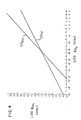
- thermochemical diagram for the oxidation of carbon is shown in FIG. 4.
- 1100°K (823°C) and at a partial pressure of oxygen 10 ⁇ 10 atmosphere i.e. the equivalent partial pressure of oxygen when H2O/H2 ⁇ 104
- the equilibrium partial pressure of CO2 is ⁇ 107 atmosphere.
- carbon particles buried in glass and exposed to oxygen having chemical potential equivalent to a partial pressure of 10 ⁇ 10 atmosphere will oxidize until the pressure of CO2 builds to 107 atmosphere.
- Such reaction and the bubbles that form is apparently the major cause of low density in glass-ceramic.
- the conditions stated above are insured by 1) removing H2O from the system, and 2) increasing the H2 content in the ambient.
- the latter temperature is chosen to reduce densification of the glass during drying.
Landscapes
- Engineering & Computer Science (AREA)
- Chemical & Material Sciences (AREA)
- Ceramic Engineering (AREA)
- Inorganic Chemistry (AREA)
- Manufacturing & Machinery (AREA)
- Microelectronics & Electronic Packaging (AREA)
- Production Of Multi-Layered Print Wiring Board (AREA)
- Laminated Bodies (AREA)
- Compositions Of Oxide Ceramics (AREA)
Applications Claiming Priority (2)
| Application Number | Priority Date | Filing Date | Title |
|---|---|---|---|
| US92997586A | 1986-11-12 | 1986-11-12 | |
| US929975 | 1986-11-12 |
Publications (2)
| Publication Number | Publication Date |
|---|---|
| EP0267602A2 true EP0267602A2 (fr) | 1988-05-18 |
| EP0267602A3 EP0267602A3 (fr) | 1990-08-01 |
Family
ID=25458774
Family Applications (1)
| Application Number | Title | Priority Date | Filing Date |
|---|---|---|---|
| EP87116673A Withdrawn EP0267602A3 (fr) | 1986-11-12 | 1987-11-11 | Procédé pour la fabrication d'une structure multicouche à haute densité en céramique de verre ayant des conducteurs métalliques |
Country Status (2)
| Country | Link |
|---|---|
| EP (1) | EP0267602A3 (fr) |
| JP (1) | JPS63128791A (fr) |
Cited By (5)
| Publication number | Priority date | Publication date | Assignee | Title |
|---|---|---|---|---|
| FR2643364A1 (fr) * | 1989-02-22 | 1990-08-24 | Air Liquide | Procede d'elaboration de composants multicouches ceramique-metal et appareil pour sa mise en oeuvre |
| GB2229572A (en) * | 1989-03-14 | 1990-09-26 | Oxley Dev Co Ltd | Ceramic multilayer structure |
| EP0352211A3 (fr) * | 1988-07-18 | 1991-11-21 | International Business Machines Corporation | Enlèvement de carbone de substrats stratifiés céramiques |
| US5682018A (en) * | 1991-10-18 | 1997-10-28 | International Business Machines Corporation | Interface regions between metal and ceramic in a metal/ceramic substrate |
| EP0871565A4 (fr) * | 1994-12-16 | 1999-06-02 | Ceramic Packaging Inc | Procede de preparation d'une structure multicouche isolee |
Families Citing this family (1)
| Publication number | Priority date | Publication date | Assignee | Title |
|---|---|---|---|---|
| JP4533129B2 (ja) * | 2004-12-28 | 2010-09-01 | 日本特殊陶業株式会社 | 配線基板の製造方法 |
Family Cites Families (4)
| Publication number | Priority date | Publication date | Assignee | Title |
|---|---|---|---|---|
| US4234367A (en) * | 1979-03-23 | 1980-11-18 | International Business Machines Corporation | Method of making multilayered glass-ceramic structures having an internal distribution of copper-based conductors |
| JPS59995A (ja) * | 1982-06-16 | 1984-01-06 | 富士通株式会社 | 銅導体多層構造体の製造方法 |
| US4474731A (en) * | 1983-03-28 | 1984-10-02 | International Business Machines Corporation | Process for the removal of carbon residues during sintering of ceramics |
| US4671928A (en) * | 1984-04-26 | 1987-06-09 | International Business Machines Corporation | Method of controlling the sintering of metal particles |
-
1987
- 1987-07-20 JP JP62179285A patent/JPS63128791A/ja active Granted
- 1987-11-11 EP EP87116673A patent/EP0267602A3/fr not_active Withdrawn
Cited By (7)
| Publication number | Priority date | Publication date | Assignee | Title |
|---|---|---|---|---|
| EP0352211A3 (fr) * | 1988-07-18 | 1991-11-21 | International Business Machines Corporation | Enlèvement de carbone de substrats stratifiés céramiques |
| FR2643364A1 (fr) * | 1989-02-22 | 1990-08-24 | Air Liquide | Procede d'elaboration de composants multicouches ceramique-metal et appareil pour sa mise en oeuvre |
| EP0384835A1 (fr) * | 1989-02-22 | 1990-08-29 | L'air Liquide, Societe Anonyme Pour L'etude Et L'exploitation Des Procedes Georges Claude | Procédé d'élaboration de composants multicouches céramique-métal et appareil pour sa mise en oeuvre |
| US5082606A (en) * | 1989-02-22 | 1992-01-21 | L'air Liquide, Societe Anonyme Pour L'etude Et L'exploitation Des Procedes Georges Claude | Process for producing ceramic-metal multilayer components and apparatus for carrying out the process |
| GB2229572A (en) * | 1989-03-14 | 1990-09-26 | Oxley Dev Co Ltd | Ceramic multilayer structure |
| US5682018A (en) * | 1991-10-18 | 1997-10-28 | International Business Machines Corporation | Interface regions between metal and ceramic in a metal/ceramic substrate |
| EP0871565A4 (fr) * | 1994-12-16 | 1999-06-02 | Ceramic Packaging Inc | Procede de preparation d'une structure multicouche isolee |
Also Published As
| Publication number | Publication date |
|---|---|
| EP0267602A3 (fr) | 1990-08-01 |
| JPS63128791A (ja) | 1988-06-01 |
| JPH0150120B2 (fr) | 1989-10-27 |
Similar Documents
| Publication | Publication Date | Title |
|---|---|---|
| US5004640A (en) | Multilayered ceramic substrates and method for manufacturing the same | |
| EP0098067B1 (fr) | Procédé pour fabriquer une structure à multi-couches en verre-céramique comprenant des conducteurs basés sur le cuivre | |
| US4795512A (en) | Method of manufacturing a multilayer ceramic body | |
| JPS6230638A (ja) | ガラス−セラミツク複合基板の製造方法 | |
| EP0505307A2 (fr) | Procédé pour fabriquer des structures scellées en verre-céramique cuit | |
| EP0352211B1 (fr) | Enlèvement de carbone de substrats stratifiés céramiques | |
| EP0267602A2 (fr) | Procédé pour la fabrication d'une structure multicouche à haute densité en céramique de verre ayant des conducteurs métalliques | |
| US5139975A (en) | Sintering arrangement for enhancing removal of carbon from ceramic substrate laminates | |
| US5053361A (en) | Setter tile for use in sintering of ceramic substrate laminates | |
| JPH06268375A (ja) | 多層配線セラミック基板の製造方法 | |
| JP2506520B2 (ja) | 多層セラミック物品を熱加工する方法 | |
| JPH06169174A (ja) | 多層セラミック構造物からのバインダー除去 | |
| EP0264088B1 (fr) | Procédé de cuisson en atmosphère contrôlée | |
| US4891246A (en) | Controlled atmosphere firing process | |
| JPH02277282A (ja) | ハイブリッド回路基体上での厚フィルム電気部品の製造方法 | |
| JP2970781B2 (ja) | 積層コンデンサの製造方法 | |
| JPS61292392A (ja) | セラミツク配線基板の製造方法 | |
| JPS62145896A (ja) | セラミツク銅多層配線基板の製造方法 | |
| JPH0321109B2 (fr) | ||
| JPH0320914B2 (fr) | ||
| JPS63292692A (ja) | 低温焼成多層セラミック基板の製造方法 | |
| JPS62198198A (ja) | セラミツク多層配線基板の製造方法 | |
| JPH02279577A (ja) | セラミック基板の製造方法 | |
| JPH03285208A (ja) | 導電性ペースト | |
| JPH09252181A (ja) | 多層セラミックス回路基板の製造方法 |
Legal Events
| Date | Code | Title | Description |
|---|---|---|---|
| PUAI | Public reference made under article 153(3) epc to a published international application that has entered the european phase |
Free format text: ORIGINAL CODE: 0009012 |
|
| AK | Designated contracting states |
Kind code of ref document: A2 Designated state(s): DE FR GB |
|
| 17P | Request for examination filed |
Effective date: 19880910 |
|
| PUAL | Search report despatched |
Free format text: ORIGINAL CODE: 0009013 |
|
| AK | Designated contracting states |
Kind code of ref document: A3 Designated state(s): DE FR GB |
|
| 17Q | First examination report despatched |
Effective date: 19920219 |
|
| STAA | Information on the status of an ep patent application or granted ep patent |
Free format text: STATUS: THE APPLICATION IS DEEMED TO BE WITHDRAWN |
|
| 18D | Application deemed to be withdrawn |
Effective date: 19930323 |
|
| RIN1 | Information on inventor provided before grant (corrected) |
Inventor name: CHANCE, DUDLEY AUGUSTUS Inventor name: GOLAND, DAVID BRIAN |