EP0267612B1 - Temporisateur/compteur utilisant un bloc à registres - Google Patents
Temporisateur/compteur utilisant un bloc à registres Download PDFInfo
- Publication number
- EP0267612B1 EP0267612B1 EP87116725A EP87116725A EP0267612B1 EP 0267612 B1 EP0267612 B1 EP 0267612B1 EP 87116725 A EP87116725 A EP 87116725A EP 87116725 A EP87116725 A EP 87116725A EP 0267612 B1 EP0267612 B1 EP 0267612B1
- Authority
- EP
- European Patent Office
- Prior art keywords
- count
- timer
- register
- value
- input
- Prior art date
- Legal status (The legal status is an assumption and is not a legal conclusion. Google has not performed a legal analysis and makes no representation as to the accuracy of the status listed.)
- Expired - Lifetime
Links
Images


Classifications
-
- G—PHYSICS
- G06—COMPUTING OR CALCULATING; COUNTING
- G06F—ELECTRIC DIGITAL DATA PROCESSING
- G06F9/00—Arrangements for program control, e.g. control units
- G06F9/06—Arrangements for program control, e.g. control units using stored programs, i.e. using an internal store of processing equipment to receive or retain programs
- G06F9/46—Multiprogramming arrangements
- G06F9/48—Program initiating; Program switching, e.g. by interrupt
- G06F9/4806—Task transfer initiation or dispatching
- G06F9/4812—Task transfer initiation or dispatching by interrupt, e.g. masked
- G06F9/4825—Interrupt from clock, e.g. time of day
-
- G—PHYSICS
- G06—COMPUTING OR CALCULATING; COUNTING
- G06F—ELECTRIC DIGITAL DATA PROCESSING
- G06F1/00—Details not covered by groups G06F3/00 - G06F13/00 and G06F21/00
- G06F1/04—Generating or distributing clock signals or signals derived directly therefrom
- G06F1/14—Time supervision arrangements, e.g. real time clock
Definitions
- the present invention relates to a timer/counter incorporated in a microcomputer, and more specifically to such a timer/counter which can realize a plurality of timer functions by using a plurality of registers in a software manner.
- a timer/counter is adapted to respond to a clock signal from an internal or external clock source so as to increment the value of count in a counter, and to compare the incremented count value with a predetermined value set in a timer register at each time of increment. Then, the timer/counter will generate an interrupt signal which the incremented count value has become consistent with the predetermined value, and at the same time, clear the counter so that the counter can count from its initial value. Furthermore, the timer/counter can execute a capture operation in which the count value in the counter is transferred and held in the timer register in response to a trigger signal which is generated at a predetermined timing or period.
- the timer/counter can be used as a timer by setting in the timer register a value corresponding to a desired time interval.
- the count value of the counter will represent the pulse number of the external signal. Therefore, the timer/counter can function as an event counter for counting the number of observed events.
- the timer/counter is used to function as a timer and also to cause to the timer register to capture the count value of the counter in response to an external signal as the trigger signal, it is possible to measure the period of occurrence of the external signal, and therefore it is possible to know an operation speed or a position of an external equipment which generates the external signal.
- the timer/counter can realize various functions by selecting a clock signal source and by controlling the comparison operation and/or the capture operation.
- the various functions can be executed at a real time in parallel to a program operation of the microcomputer. Therefore, the timer/counter has already held an important position in the field of existing single chip microcomputers.
- timer/counters have been used as (1) an internal timer for stepwise changing a phase of a magnetic field applied to a coil of a step motor for moving a printing head; (2) a position detection counter for determining the position of the printing head, (3) a one-shot timer used to control the application time of an electric current to a printing solenoid, etc.
- an internal timer for stepwise changing a phase of a magnetic field applied to a coil of a step motor for moving a printing head
- a position detection counter for determining the position of the printing head
- a one-shot timer used to control the application time of an electric current to a printing solenoid
- the timer/counter is composed of a counter or count register for holding a count value, an incrementer for reading the count value of the counter register so as to increment the count value, and a latch for latching the incremented value from the incrementer and updating the content of the count register by the incremented value.
- the timer/counter comprises a timer register for storing a predetermined value to be compared with the value of the count register or for capturing the value of the count register, and a comparator for comparing the value of the count register with the preset value of the timer register so as to generate an interrupt signal when both the values coincide with each other. Operations of the above various circuits are controlled by a controller. Then, all of the above mentioned various circuits are constituted of random logic circuits, i.e., hardware.
- the random logic circuit needs a large number of transistors, and also, the transistors themselves used for the random logic circuit are of a relatively large size. Therefore, in the case that the random logic circuit is realized on an integrated circuit, a considerably large chip area is required. As a result, if a plurality of timer/counters are formed on a single chip, the chip area must be increased, and so, the cost of the single chip computer would inevitably become high. In addition, the random logic circuit has only a limited function, and therefore, when the numbers of the count registers and the timer registers must be changed, it is necessary to refashion the whole of the circuits, which needs even redesigning of mask patterns used in fabrication of integrated circuits.
- US-A-4 024 510 discloses an apparatus for timing a variety of timing signals comprising a functional control logic, an accumulator storage, a constant storage, output and input data registers, an increment and data select circuit, a comparator and a storage and data control logic to reset the accumulator register if the accumulator signal is equal to a stored constant.
- Still another object of the invention is to provide a timer/counter having a high feasibility.
- a plurality of count registers and timer registers are formed in the register block, i.e., a memory, and a count values held in the respective count registers are sequentially read out, and incremented by one incrementer, and then, returned to the same count registers. Accordingly, it is no longer necessary to a plurality of timer/counters each composed of a random logic circuit and each including at least one count register, one timer register, an incrementer and a comparator. Therefore, the chip area required for the timer/counter in accordance with the present invention is greatly decreased as compared with the conventional one, and so, a microcomputer incorporating the timer/counter in accordance with the present invention can be inexpensively fabricated on a small area chip.
- the count registers and the timer registers in the register block can be constituted of the same memory elements. Therefore, the number of the count registers and the timer registers can be easily changed without needing a substantial change of hardware. Namely, the timer/register in accordance with the present invention can have a high feasibility.
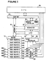
- one embodiment of the timer/counter in accordance with the present invention comprises a register block 10 including a plurality of count registers and a corresponding number of timer registers, each of which is constituted of an array of memory cells.
- the register block 10 includes a buffer circuit 12 for reading/writing of the memory cells, four count registers 14A, 14B, 14C and 14D each composed of an array of memory cells, and four timer registers 16A, 16B, 16C and 16D each also composed of an array of memory cells.
- the count registers and the timer registers can be formed of a content addressable memory (called "CAM" hereinafter).
- the count registers 14A to 14D have the same construction and the same function and operate in the same manner
- the timer registers 16A, 16B, 16C and 16D have the same construction and the same function and operate in the same manner.
- the register block 10 is coupled through an internal bus 18 to a data bus 20 and an incrementer 22, which operates to receive data on the internal bus 18 and to output an incremented data to a latch 24.
- This latch 24 outputs the latched data to the internal bus 18 so that the data will be written into a register of the register block 10.
- a coincidence flag 26 is coupled to receive coincidence signals 28A, 28B, 28C and 28D from the respective timer registers 16A, 16B, 16C and 16D and to correspondingly output interrupt signals 30A, 30B, 30C and 30D to a clear controller 32.
- This clear controller 32 generates a clear signal 34 to the latch 24 in response to the received interrupt signal.
- the shown time/counter also includes an operation controller 36 coupled to the data bus 20 to receive a control information from a central processing unit (called "CPU” hereinafter) 38.
- This operation controller 36 includes therein a mode register 40 designating an operation mode of the timer/counter, and controls the operation mode and the operation timing of various circuits in the timer/counter. Further, the CPU 38 receives the interrupt signals 30A to 30D.
- the timer counter operates as a timer
- a count number and control information are transferred through the data bus 20 in accordance with a program operation executed by the CPU 38, and then stored in the timer register 16A of the register block 10 and the operation controller 36.
- the mode register 40 of the operation controller 36 is set to a comparison operation, and it is assumed that a comparison value "n" is set in the timer register 16A.
- the operation controller 36 will generate operation control signals to various circuits and selects an input clock signal (from internal clock sources or external clock sources).
- the count operations of the respective registers are sequentially executed by using the incrementer 22, the internal bus 18, etc. in a time division manner in synchronism with a reference clock signal CL.
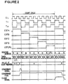
- one unitary count-up operation of each count register is executed for a time period corresponding to two reference clocks (this period will be called “count stage” hereinafter). Therefore, a sequence of count operations of the four count registers 14A to 14D and an access operation of the CPU 38 are carried out for five count stages (i.e., for the time of ten reference clocks), which constitute one count cycle.
- five count stage signals CSTA, CSTB, CSTC, CSTD and CSTCPU are generated from the reference clock.
- count stage signals CST are sequentially made active for one count stage without overlapping with each other, as shown in Figure 2, and are respectively assigned to the count registers 14A to 14D and the CPU 38. Therefore, if the CSTA signal is active, i.e., at a high level, the count operation is executed for the count register 14A.
- the reference clock CL is frequency-divided to generate a first timing signal T1 indicative of a first half of each count stage and a second timing signal T2 indicative of a second half of each count stage.
- the operation of various circuits is timed on the basis of the reference clock CL and the two timing signals T1 and T2.
- the data “n-1” is read out from the count register 14A, and incremented to "n” by the incrementer 22 in the period of the timing signal T1.
- the incremented data “n” is latched in the latch 24 in the period of the same timing signal T1.
- the content of the latch 24 is outputted to the internal bus 18, and on the other hand, the internal data lines of the count register 14A are precharged at the high level time of the clock CL during the high level period of the timing signal T2, and then, the count register 14A is rewritten with the data on the internal bus 18, i.e., the incremented data "n" in the above example at a low level time of the clock CL during the high level period of the same timing signal T2.
- the data on the internal bus 18 is compared with the content previously set in the corresponding timer register 16A, and if they are coincident with each other, the timer register 16A generates an active or high level coincidence signal 28A, which will set the coincidence flag 26. As a result, the coincidence flag 26 generates a high level interrupt signal 30A to the clear controller 32 and the CPU 38.
- the clear controller 32 In the corresponding count stage of the next count cycle, the clear controller 32 generates a clear signal 34 to the latch 24.
- the content of the count register 14A is read out to the incrementer 22 at the timing signal T1 so as to cause it to output an incremented or unincremented data
- the latch 24 since the latch 24 outputs data of "0" to the internal bus in accordance with the clear signal 34 regardless of the output of the incrementer 22, the data of "0" is written to the count register 14A. In other words, the count register 14A is cleared.
- the coincidence flag 26 is reset, and the clear signal 34 is returned to a low level at the completion of the count stage.
- the CPU 38 can access the timer registers 16A to 16D in the period of the count stage CSTCPU assigned to the access operation of the CPU 38. Specifically, at a high level time of the reference clock CL during the high level period of the timing signal T1, the bus 20 is precharged and the CPU 38 transfers the register designation information fed through the bus 20 to the register block 10 as an address information, and at the succeeding low level period of the same clock CL, it causes the register block 10 to output the content at the designated address to the bus 20. In the writing, data is written to the register block through the data bus 20 at the low level period of the reference clock CL.
- the registers of the register block 10 are formed of an array of CAM cells.
- FIG 3 there is shown a circuit diagram of one CAM cell.
- the shown CAM cell includes ten transistors Q 1 to Q 10 connected as shown in Figure 3, and has a pair of input/output lines D and D for a truth value and an inversion value, a cell selection signal line S and a data discrimination output line C.
- Transistors Q 1 and Q 3 are cross-connected to each other as shown to form a flipflop which can be inverted in response to an inputted data, and connected through respective load transistors Q 2 and Q 4 between a voltage V DD and the ground.
- a node between Q 1 and Q 2 and another node between Q 3 and Q 4 are respectively connected to the pair of data input/output lines D and D through transistors Q 5 and Q 6 whose gates are commonly connected to the selection signal line S.
- the flipflop thus formed stores a bit of information by its internal condition.
- the cell selection line S is rendered active so as to put the transistors Q 5 and Q 6 in a conductive condition, with the result that the data held in the flipflop is read out to the pair of input/output lines D and D .
- the truth value and the inversion value of data to be written are supplied to the pair of input/output lines D and D , respectively, and the cell selection line S is made active so as to bring the transistors Q 5 and Q 6 into a conductive condition.
- the internal condition is forcibly changed to conform with the inputted data.
- a circuit for discriminating coincidence between the input data and the stored data includes four transistors Q 7 , Q 8 , Q 9 and Q 10 .
- a pair of transistors Q 7 and Q 8 are connected in series between the data discrimination output line C and the ground, and connected at their gates to the truth value input/output line D and the node between the transistors Q 3 and Q 4 , respectively.
- Another pair of transistors Q 9 and Q 10 are connected in series between the data discrimination output line C and the ground, and connected at their gates the inversion value input/output line D and the node between the transistor Q 1 and Q 2 .
- This discrimination circuit generates the coincidence signal in response to the inputted data and the stored data, as described in the following Table.
- the above Table is based on the assumption that a condition in which the line C is at ground level represents a logic value "0" and another condition in which the line C is isolated from the ground indicates a logic value "1".
- the circuit generates at the line C an exclusive OR signal representative of incoincidence between the input data on the input/output lines D and D and the stored data held in the flipflop. Specifically, the discrimination circuit generates the logic value "1" on the line C not only when the input data is perfectly coincident with the stored data both in the truth value and in the inversion value, but also when both of the input data D and D are at a logic "0" regardless of the stored data. In the latter case, the result of the comparison is masked.
- the discrimination circuit generates the logic value "0" on the line C not only when the input data is completely different from the stored data both in the truth value and in the inversion value, but also both of the input data D and D are at a logic level "1". Namely, in the latter case, the discrimination result of the incoincidence is generated unconditionally.
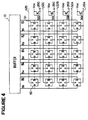
- FIG 4 there is shown a block diagram of the timer registers 16A to 16D, each of which is composed of an array of five CAM cells 50 shown in Figure 3.
- CAM cells 50 of the respective cell arrays positioned at the same bit place are connected in parallel at their respective inputs/outputs D and D so as to receive the same place bit data (B 1 and B 1 , B 2 and B 2 , B 3 and B 3 , B 4 and B 4 or B 5 and B 5 ) from the buffer circuit 12.
- the selection inputs S and the discrimination outputs C of the respective CAM cells 50 included in the same array are respectively connected commonly to a selection signal line 52 (52A, 52B, 52C or 52D) and the coincidence signal line 28 (28A, 28B, 28C or 28D) which is pulled up to V DD through a load transistor 56 (56A, 56B, 56C or 56D). Therefore, when all the discrimination signals C of the CAM cells in the same array are at the logic value "1" (i.e., isolated from the ground), the coincidence signal line 28 will generate a high level signal of the logic value "1". But, if any one of the CAM cells in the same array generates the logic value "0" as the discrimination signal C (i.e., shortcircuited to the ground), the coincidence signal line 28 is brought to a low level of the logic value "0".
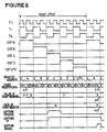
- FIG. 5 there is shown an array of CAM cells which can be used as the count timer and also as the timer register.
- the shown five CAM cells 50 are connected in a manner similar to that shown in Figure 4.
- To the selection signal line 52 is connected an output of an OR gate 58 which is connected to receive at its one input a selection address decoder output signal 60 and at its other input an output of an AND gate 62.
- the signal 60 is applied when the CPU 38 accesses the register block, for example, to set a comparison value to the timer register.
- the AND gate 62 receives at its first input the reference clock CL through an inverter 64, at its second input the timing signal T2, at its third input the count stage signal CST, and at its fourth input a Q output of a capture flipflops 66 of the set/reset type.
- This flipflop has a set input connected to receive a capture trigger signal, and a reset input connected to the output of the AND gate 62.
- the mode register 40 is set to the capture operation, and data "n" is set to the timer register 16A.
- the selection of the count registers in correspondence to the count stage and the increment operation are executed similarly to the comparison operation. If a capture trigger signal 68 is generated (in this embodiment, at a second count stage after the count stage in which the designated count register 16A is incremented to "n"), the capture flipflop 66 is set, so that the Q output is brought to a high level. This condition is maintained after the next corresponding count stage is executed.
- the capture signal is applied from the AND gate 62 through the OR gate 58 and the line 52 to the selection signal lines S of the respective CAM cells.
- the count value is outputted from the latch 24 to the data lines D and D in the register block 10, and then is written to the selected count register 14A and also to the selected timer register 16A.
- the value (n+1) of the count register 14A which has been rewritten at the corresponding count stage just after the capture trigger 68 is generated, is also stored to the corresponding timer register 16A.
- a plurality of counters can be realized in the timer/counter which can be constructed with a relatively small number of transistors, because it is not necessary to prepare one incrementer, one comparator, etc. in the form of logic circuits for each of counters. Therefore, the timer/counter can be realized at a small area chip at an inexpensive cost. Further, the count registers and the timer registers are prepared in the register block, i.e., in a memory, and the count registers are sequentially incremented in a programmed operation. Therefore, the number of these registers can be freely changed. Particularly, each timer register is formed of an array of CAM cells having a coincidence detection function, and so, there is required no comparator composed of a random logic. In addition, the array of CAM cells can be used as the count register. Accordingly, the timer/counter has a good feasibility.
Landscapes
- Engineering & Computer Science (AREA)
- Theoretical Computer Science (AREA)
- Software Systems (AREA)
- Physics & Mathematics (AREA)
- General Engineering & Computer Science (AREA)
- General Physics & Mathematics (AREA)
- Microcomputers (AREA)
- Programmable Controllers (AREA)
- Debugging And Monitoring (AREA)
Claims (3)
- Horloge/compteur comprenant :caractérisé en ce que chaque registre d'horloge (16A-16D) inclut une matrice de cellules de mémoire adressables par le contenu, de sorte que chaque registre d'horloge a une fonction de comparaison permettant l'exécution d'une détection de coïncidence entre la valeur sur le bus interne (18) devant être écrite dans un registre de comptage correspondant et le contenu antérieurement fixé dans le registre d'horloge lui-même, à chaque phase de comptage correspondante d'un cycle de comptage au cours duquel la valeur sur le bus interne (18) doit écrite dans un registre de comptage correspondant,un contrôleur d'exploitation (36) couplé à un bus de données (20) pour recevoir une information de commande permettant de générer des signaux de commande destinés à un mode opératoire sélectionné de l'horloge/compteur,un bloc de registres (10) couplé à un bus interne (18) incluantune pluralité de registres de comptage (14A-14D),un nombre correspondant de registres d'horloge (16A-16D) mémorisant diverses valeurs fixées, etun circuit tampon (12) par l'intermédiaire duquel les registres de comptage et les registres d'horloge sont couplés audit bus interne (18) ;un circuit d'incrémentation (22) commandé par le contrôleur d'exploitation (36) et couplé au bus interne pour recevoir une valeur par le bus interne, et couplé à un circuit à verrouillage (24) afin de délivrer, soit la valeur reçue ayant été incrémentée, si une horloge de comptage est active, soit la valeur reçue n'ayant pas été incrémentée, dans le cas inverse ;ledit circuit à verrouillage (24) étant commandé par le contrôleur d'exploitation (36) pour verrouiller la valeur délivrée par le circuit d'incrémentation (22) de manière à délivrer la valeur verrouillée, par l'intermédiaire du bus interne (18), au circuit tampon (12),le circuit tampon (12), le circuit d'incrémentation (22) et le circuit à verrouillage (24) étant commandés par le contrôleur d'exploitation (36) de manière à exécuter, de façon séquentielle et cyclique, sur les registres de comptage respectifs, par répartition dans le temps, une opération telle qu'une valeur est lue à partir de l'un des registres de comptage et transmise au bus interne (18) de manière à être reçue par le circuit d'incrémentation (22), et la valeur délivrée par le circuit d'incrémentation (22) est verrouillée dans le circuit à verrouillage, puis la valeur mémorisée dans le circuit à verrouillage est écrite dans le même registre de comptage, ladite opération étant respectivement exécutée sur un registre de comptage au cours d'une phase de comptage correspondante d'un cycle de comptage ;Un indicateur de coïncidence (26) couplé au bloc de registres (10) et ayant une pluralité de sorties qui correspondent à la pluralité de registres d'horloge, respectivement, chacune d'entre elles délivrant un signal de sortie qui est amené à un niveau actif lorsque le registre d'horloge correspondant détecte une coïncidence de données, de sorte que si la valeur devant être écrite dans un registre de comptage correspondant coïncide avec le contenu antérieurement fixé dans le registre d'horloge correspondant, l'une correspondante de la pluralité de sorties dudit indicateur de coïncidence (26) est amenée à un niveau actif par le registre d'horloge correspondant,un contrôleur d'effacement (32) couplé à l'indicateur de coïncidence de manière à effacer le registre de comptage ayant une valeur de comptage en coïncidence avec la valeur du registre d'horloge correspondant,ledit contrôleur d'effacement (32) effaçant le verrouillage lors de la phase de comptage correspondante du cycle de comptage qui suit le cycle de comptage au cours duquel la coïncidence est détectée, de sorte que le contenu effacé du circuit à verrouillage est chargé et écrit dans le registre de comptage correspondant.
- Horloge/compteur selon la revendication 1, dans laquelle chacune des cellules de mémoire inclut une bascule ayant des premières et secondes entrées/sorties de données recevant une paire de signaux de données qui sont en opposition de phase l'un à l'autre, une paire de transistors de commutation (Q5, Q6) respectivement connectés entre la première entrée/sortie de la bascule et une entrée/sortie de signaux de données logiques (D), et entre la seconde entrée/sortie de la bascule et une entrée/sortie de signaux de données d'inversion (
D ), ces transistors de commutation (Q5, Q6) étant connectés pour recevoir à leurs électrodes de commande le même signal de sélection (S), et une paire de circuits OU exclusif à deux entrées connectés à leurs sorties respectives à une sortie de détection de coïncidence (C), l'un des circuits OU exclusif étant connecté, à sa première entrée, à l'entrée/sortie de signaux de données logiques (D), et, à son autre entrée, à la seconde entrée/sortie de la bascule, et l'autre circuit OU exclusif étant connecté, à sa première entrée, à l'entrée/sortie de signaux de données d'inversion (D ) , et, à son autre entrée, à la première entrée/sortie de la bascule, de sorte que, le signal de sélection (S) étant actif, les données peuvent être lues et être écrites dans la bascule, et le signal de sélection (S) étant inactif, les circuits OU exclusif génèrent, à la sortie de détection de coïncidence (C), un signal indiquant si les données d'entrée sont identiques ou non aux données fixées dans la bascule. - Horloge/compteur selon la revendication 1, dans laquelle le bloc de registres (10) fonctionne en réponse à un signal de capture de manière à ce que la valeur incrémentée soit écrite non seulement dans l'un des registres de comptage mais également dans un registre d'horloge correspondant.
Applications Claiming Priority (2)
| Application Number | Priority Date | Filing Date | Title |
|---|---|---|---|
| JP270144/86 | 1986-11-12 | ||
| JP61270144A JPS63123218A (ja) | 1986-11-12 | 1986-11-12 | タイマ/カウンタ回路 |
Publications (3)
| Publication Number | Publication Date |
|---|---|
| EP0267612A2 EP0267612A2 (fr) | 1988-05-18 |
| EP0267612A3 EP0267612A3 (fr) | 1990-04-25 |
| EP0267612B1 true EP0267612B1 (fr) | 1998-08-26 |
Family
ID=17482158
Family Applications (1)
| Application Number | Title | Priority Date | Filing Date |
|---|---|---|---|
| EP87116725A Expired - Lifetime EP0267612B1 (fr) | 1986-11-12 | 1987-11-12 | Temporisateur/compteur utilisant un bloc à registres |
Country Status (4)
| Country | Link |
|---|---|
| US (1) | US4939755A (fr) |
| EP (1) | EP0267612B1 (fr) |
| JP (1) | JPS63123218A (fr) |
| DE (1) | DE3752211T2 (fr) |
Cited By (1)
| Publication number | Priority date | Publication date | Assignee | Title |
|---|---|---|---|---|
| CN103455310A (zh) * | 2012-05-29 | 2013-12-18 | 中兴通讯股份有限公司 | 信号量等待接口定时方法及装置 |
Families Citing this family (34)
| Publication number | Priority date | Publication date | Assignee | Title |
|---|---|---|---|---|
| US5081297A (en) * | 1986-05-06 | 1992-01-14 | Grumman Aerospace Corporation | Software reconfigurable instrument with programmable counter modules reconfigurable as a counter/timer, function generator and digitizer |
| JP2656303B2 (ja) * | 1988-06-23 | 1997-09-24 | 株式会社東芝 | ディジタル形保護継電装置 |
| JP2656304B2 (ja) * | 1988-06-23 | 1997-09-24 | 株式会社東芝 | ディジタル形保護継電装置 |
| JPH0210417A (ja) * | 1988-06-28 | 1990-01-16 | Fujitsu Ltd | カウンタ回路 |
| JPH0296963A (ja) * | 1988-10-03 | 1990-04-09 | Hitachi Ltd | 半導体集積回路装置 |
| US5012435A (en) * | 1988-11-17 | 1991-04-30 | International Business Machines Corporation | Multiple event timer circuit |
| US4984169A (en) * | 1989-03-23 | 1991-01-08 | Milliken Research Corp. | Data loading and distributing process and apparatus for control of a patterning process |
| FR2646034B1 (fr) * | 1989-04-12 | 1991-06-07 | Cegelec | Matrice de compteurs synchrones multiplexes pour circuit integre |
| EP0554485B1 (fr) * | 1992-02-05 | 1997-11-19 | Siemens Aktiengesellschaft | Méthode de mise à jour des cellules de rythmeur d'un appareil d'automatisation et appareil d'automatisation |
| EP0579324B1 (fr) * | 1992-07-17 | 1998-12-30 | Koninklijke Philips Electronics N.V. | Microprocesseur muni de moyens de comptage de rythmes à registres fournissant dans une position de comptage prédéterminée un signal de commande de forme réglable et système d'interruption hiérarchique destiné à être utilisé avec ceux-ci |
| EP0689141A3 (fr) * | 1994-06-20 | 1997-10-15 | At & T Corp | Support en hardware basé sur des interruptions pour profiler la performance de systèmes |
| KR100419549B1 (ko) * | 1995-11-27 | 2004-06-12 | 코닌클리케 필립스 일렉트로닉스 엔.브이. | 파라미터화가능모듈,전자회로,제어기시스템,회로합성방법 |
| US5784627A (en) * | 1996-01-24 | 1998-07-21 | Advanced Micro Devices, Inc. | Integrated timer for power management and watchdog functions |
| US6076157A (en) * | 1997-10-23 | 2000-06-13 | International Business Machines Corporation | Method and apparatus to force a thread switch in a multithreaded processor |
| US6567839B1 (en) | 1997-10-23 | 2003-05-20 | International Business Machines Corporation | Thread switch control in a multithreaded processor system |
| US6212544B1 (en) | 1997-10-23 | 2001-04-03 | International Business Machines Corporation | Altering thread priorities in a multithreaded processor |
| US6697935B1 (en) | 1997-10-23 | 2004-02-24 | International Business Machines Corporation | Method and apparatus for selecting thread switch events in a multithreaded processor |
| KR100471137B1 (ko) * | 1997-10-31 | 2005-06-07 | 삼성전자주식회사 | 단축된 레지스터 클리어 인스트럭션 실행 사이클을 갖는 데이터처리 장치 |
| US6314524B1 (en) * | 1999-03-18 | 2001-11-06 | Intervoice Limited Partnership | Repetitive interval timing |
| US6232808B1 (en) * | 1999-03-18 | 2001-05-15 | Intervoice Limited Partnership | Irregular interval timing |
| US7487200B1 (en) | 1999-09-23 | 2009-02-03 | Netlogic Microsystems, Inc. | Method and apparatus for performing priority encoding in a segmented classification system |
| US6934795B2 (en) | 1999-09-23 | 2005-08-23 | Netlogic Microsystems, Inc. | Content addressable memory with programmable word width and programmable priority |
| US6567340B1 (en) | 1999-09-23 | 2003-05-20 | Netlogic Microsystems, Inc. | Memory storage cell based array of counters |
| US7110407B1 (en) | 1999-09-23 | 2006-09-19 | Netlogic Microsystems, Inc. | Method and apparatus for performing priority encoding in a segmented classification system using enable signals |
| US7272027B2 (en) | 1999-09-23 | 2007-09-18 | Netlogic Microsystems, Inc. | Priority circuit for content addressable memory |
| US7143231B1 (en) | 1999-09-23 | 2006-11-28 | Netlogic Microsystems, Inc. | Method and apparatus for performing packet classification for policy-based packet routing |
| US6944709B2 (en) | 1999-09-23 | 2005-09-13 | Netlogic Microsystems, Inc. | Content addressable memory with block-programmable mask write mode, word width and priority |
| US20030191151A1 (en) * | 2001-10-26 | 2003-10-09 | Imtiaz Chaudry | Albuterol and ipratropium inhalation solution, system, kit and method for relieving symptoms of chronic obstructive pulmonary disease |
| US20050091456A1 (en) * | 2003-10-23 | 2005-04-28 | Huck Jerome C. | Determining an arrangement of data in a memory for cache efficiency |
| KR101689279B1 (ko) * | 2010-09-17 | 2016-12-23 | 삼성전자주식회사 | 타이머 및 이를 포함하는 집적 회로 디바이스 |
| JP5894493B2 (ja) * | 2011-08-09 | 2016-03-30 | ルネサスエレクトロニクス株式会社 | タイミング制御装置及びそれを備えた制御システム |
| GB2502540A (en) | 2012-05-30 | 2013-12-04 | Ibm | Generating monotonically increasing time of day values in multiprocessors |
| US10416703B2 (en) * | 2017-08-10 | 2019-09-17 | Ambiq Micro, Inc. | Counter/timer array for generation of complex patterns independent of software control |
| CN116111996A (zh) * | 2023-01-30 | 2023-05-12 | 无锡艾为集成电路技术有限公司 | 一种多通道可编程负载开关电路、控制方法和电子设备 |
Family Cites Families (11)
| Publication number | Priority date | Publication date | Assignee | Title |
|---|---|---|---|---|
| US3633181A (en) * | 1969-12-23 | 1972-01-04 | Bell Telephone Labor Inc | Multiple timing list arrangement |
| US4024510A (en) * | 1975-08-28 | 1977-05-17 | International Business Machines Corporation | Function multiplexer |
| US4090239A (en) * | 1976-12-30 | 1978-05-16 | Honeywell Information Systems Inc. | Interval timer for use in an input/output system |
| US4161787A (en) * | 1977-11-04 | 1979-07-17 | Motorola, Inc. | Programmable timer module coupled to microprocessor system |
| US4222103A (en) * | 1978-09-25 | 1980-09-09 | Motorola, Inc. | Real time capture registers for data processor |
| US4220990A (en) * | 1978-09-25 | 1980-09-02 | Bell Telephone Laboratories, Incorporated | Peripheral processor multifunction timer for data processing systems |
| US4249070A (en) * | 1978-09-29 | 1981-02-03 | Gulf & Western Manufacturing Company | Counter/timer with incremental indicators |
| US4556938A (en) * | 1982-02-22 | 1985-12-03 | International Business Machines Corp. | Microcode control mechanism utilizing programmable microcode repeat counter |
| JPS5947625A (ja) * | 1982-09-13 | 1984-03-17 | Fujitsu Ltd | 入出力割り込み方式 |
| EP0175603A2 (fr) * | 1984-08-21 | 1986-03-26 | FAIRCHILD CAMERA & INSTRUMENT CORPORATION | Cellule de mémoire associative |
| US4879733A (en) * | 1988-01-28 | 1989-11-07 | Motorola, Inc. | Timer architecture for multi-task computers and for serial data decoding |
-
1986
- 1986-11-12 JP JP61270144A patent/JPS63123218A/ja active Granted
-
1987
- 1987-11-12 EP EP87116725A patent/EP0267612B1/fr not_active Expired - Lifetime
- 1987-11-12 DE DE3752211T patent/DE3752211T2/de not_active Expired - Fee Related
- 1987-11-12 US US07/119,515 patent/US4939755A/en not_active Expired - Lifetime
Cited By (1)
| Publication number | Priority date | Publication date | Assignee | Title |
|---|---|---|---|---|
| CN103455310A (zh) * | 2012-05-29 | 2013-12-18 | 中兴通讯股份有限公司 | 信号量等待接口定时方法及装置 |
Also Published As
| Publication number | Publication date |
|---|---|
| JPH056207B2 (fr) | 1993-01-26 |
| DE3752211T2 (de) | 1999-05-06 |
| DE3752211D1 (de) | 1998-10-01 |
| EP0267612A2 (fr) | 1988-05-18 |
| US4939755A (en) | 1990-07-03 |
| JPS63123218A (ja) | 1988-05-27 |
| EP0267612A3 (fr) | 1990-04-25 |
Similar Documents
| Publication | Publication Date | Title |
|---|---|---|
| EP0267612B1 (fr) | Temporisateur/compteur utilisant un bloc à registres | |
| EP0541685B1 (fr) | Memoire associative | |
| US9128894B2 (en) | Bus controller | |
| KR19990064138A (ko) | 저 전압 단일 전원 공급 플래시 메모리용 프로그램 알고리즘 | |
| JPS6242297B2 (fr) | ||
| EP0694828A2 (fr) | Processeur de données à communication sécurisée | |
| EP0364110B1 (fr) | Dispositif de mémoire à semi-conducteur ayant une mémoire à accès en série | |
| US5165029A (en) | Cache memory with test function | |
| US6078637A (en) | Address counter test mode for memory device | |
| US4016409A (en) | Longitudinal parity generator for use with a memory | |
| EP0449305B1 (fr) | Processeur de données pour la génération de signal d'impulsion en réponse à une horloge externe | |
| US5550996A (en) | ROM burst transfer continuous read-out extension method and a microcomputer system with a built-in ROM using this method | |
| US4580230A (en) | Cathode ray tube controller | |
| US5379410A (en) | Data generating apparatus generating consecutive data and having a data skip scheme and a method of operating the same | |
| EP0283230B1 (fr) | Circuit de registres | |
| EP0020972B1 (fr) | Dispositif microprocesseur commandé par programme | |
| EP0199890B1 (fr) | Circuit logique auto-séquencé | |
| US4503548A (en) | Timer with fast counter interrupt | |
| US6782467B1 (en) | Method and apparatus for fast limited core area access and cross-port word size multiplication in synchronous multiport memories | |
| EP0662691B1 (fr) | Unité de comptage pour mémoires non-volatiles | |
| JP2901828B2 (ja) | 半導体集積回路 | |
| JP3319755B2 (ja) | ブックキーピングメモリ | |
| JPH07120938B2 (ja) | パルス出力装置 | |
| JPH0697814A (ja) | プログラマブル・ロジック・アレイおよびそれを用いたマイクロコンピュータ | |
| JP2643609B2 (ja) | 割り込み制御装置 |
Legal Events
| Date | Code | Title | Description |
|---|---|---|---|
| PUAI | Public reference made under article 153(3) epc to a published international application that has entered the european phase |
Free format text: ORIGINAL CODE: 0009012 |
|
| 17P | Request for examination filed |
Effective date: 19871112 |
|
| AK | Designated contracting states |
Kind code of ref document: A2 Designated state(s): DE FR GB IT |
|
| PUAL | Search report despatched |
Free format text: ORIGINAL CODE: 0009013 |
|
| AK | Designated contracting states |
Kind code of ref document: A3 Designated state(s): DE FR GB IT |
|
| 17Q | First examination report despatched |
Effective date: 19920526 |
|
| APCB | Communication from the board of appeal sent |
Free format text: ORIGINAL CODE: EPIDOS OBAPE |
|
| APCB | Communication from the board of appeal sent |
Free format text: ORIGINAL CODE: EPIDOS OBAPE |
|
| APCB | Communication from the board of appeal sent |
Free format text: ORIGINAL CODE: EPIDOS OBAPE |
|
| APCB | Communication from the board of appeal sent |
Free format text: ORIGINAL CODE: EPIDOS OBAPE |
|
| APCB | Communication from the board of appeal sent |
Free format text: ORIGINAL CODE: EPIDOS OBAPE |
|
| APCB | Communication from the board of appeal sent |
Free format text: ORIGINAL CODE: EPIDOS OBAPE |
|
| APCB | Communication from the board of appeal sent |
Free format text: ORIGINAL CODE: EPIDOS OBAPE |
|
| APCB | Communication from the board of appeal sent |
Free format text: ORIGINAL CODE: EPIDOS OBAPE |
|
| APCB | Communication from the board of appeal sent |
Free format text: ORIGINAL CODE: EPIDOS OBAPE |
|
| APAB | Appeal dossier modified |
Free format text: ORIGINAL CODE: EPIDOS NOAPE |
|
| GRAG | Despatch of communication of intention to grant |
Free format text: ORIGINAL CODE: EPIDOS AGRA |
|
| GRAH | Despatch of communication of intention to grant a patent |
Free format text: ORIGINAL CODE: EPIDOS IGRA |
|
| GRAH | Despatch of communication of intention to grant a patent |
Free format text: ORIGINAL CODE: EPIDOS IGRA |
|
| GRAA | (expected) grant |
Free format text: ORIGINAL CODE: 0009210 |
|
| AK | Designated contracting states |
Kind code of ref document: B1 Designated state(s): DE FR GB IT |
|
| REF | Corresponds to: |
Ref document number: 3752211 Country of ref document: DE Date of ref document: 19981001 |
|
| ET | Fr: translation filed | ||
| PLBE | No opposition filed within time limit |
Free format text: ORIGINAL CODE: 0009261 |
|
| STAA | Information on the status of an ep patent application or granted ep patent |
Free format text: STATUS: NO OPPOSITION FILED WITHIN TIME LIMIT |
|
| 26N | No opposition filed | ||
| REG | Reference to a national code |
Ref country code: GB Ref legal event code: IF02 |
|
| REG | Reference to a national code |
Ref country code: GB Ref legal event code: 732E |
|
| REG | Reference to a national code |
Ref country code: FR Ref legal event code: TP |
|
| PGFP | Annual fee paid to national office [announced via postgrant information from national office to epo] |
Ref country code: DE Payment date: 20041104 Year of fee payment: 18 |
|
| PGFP | Annual fee paid to national office [announced via postgrant information from national office to epo] |
Ref country code: FR Payment date: 20041109 Year of fee payment: 18 |
|
| PGFP | Annual fee paid to national office [announced via postgrant information from national office to epo] |
Ref country code: GB Payment date: 20041110 Year of fee payment: 18 |
|
| APAH | Appeal reference modified |
Free format text: ORIGINAL CODE: EPIDOSCREFNO |
|
| PG25 | Lapsed in a contracting state [announced via postgrant information from national office to epo] |
Ref country code: IT Free format text: LAPSE BECAUSE OF NON-PAYMENT OF DUE FEES;WARNING: LAPSES OF ITALIAN PATENTS WITH EFFECTIVE DATE BEFORE 2007 MAY HAVE OCCURRED AT ANY TIME BEFORE 2007. THE CORRECT EFFECTIVE DATE MAY BE DIFFERENT FROM THE ONE RECORDED. Effective date: 20051112 Ref country code: GB Free format text: LAPSE BECAUSE OF NON-PAYMENT OF DUE FEES Effective date: 20051112 |
|
| PG25 | Lapsed in a contracting state [announced via postgrant information from national office to epo] |
Ref country code: DE Free format text: LAPSE BECAUSE OF NON-PAYMENT OF DUE FEES Effective date: 20060601 |
|
| GBPC | Gb: european patent ceased through non-payment of renewal fee |
Effective date: 20051112 |
|
| PG25 | Lapsed in a contracting state [announced via postgrant information from national office to epo] |
Ref country code: FR Free format text: LAPSE BECAUSE OF NON-PAYMENT OF DUE FEES Effective date: 20060731 |
|
| REG | Reference to a national code |
Ref country code: FR Ref legal event code: ST Effective date: 20060731 |