EP0541685B1 - Memoire associative - Google Patents
Memoire associative Download PDFInfo
- Publication number
- EP0541685B1 EP0541685B1 EP91914604A EP91914604A EP0541685B1 EP 0541685 B1 EP0541685 B1 EP 0541685B1 EP 91914604 A EP91914604 A EP 91914604A EP 91914604 A EP91914604 A EP 91914604A EP 0541685 B1 EP0541685 B1 EP 0541685B1
- Authority
- EP
- European Patent Office
- Prior art keywords
- storage
- cell
- memory
- bit
- cells
- Prior art date
- Legal status (The legal status is an assumption and is not a legal conclusion. Google has not performed a legal analysis and makes no representation as to the accuracy of the status listed.)
- Expired - Lifetime
Links
Images


Classifications
-
- G—PHYSICS
- G11—INFORMATION STORAGE
- G11C—STATIC STORES
- G11C11/00—Digital stores characterised by the use of particular electric or magnetic storage elements; Storage elements therefor
- G11C11/21—Digital stores characterised by the use of particular electric or magnetic storage elements; Storage elements therefor using electric elements
- G11C11/34—Digital stores characterised by the use of particular electric or magnetic storage elements; Storage elements therefor using electric elements using semiconductor devices
- G11C11/40—Digital stores characterised by the use of particular electric or magnetic storage elements; Storage elements therefor using electric elements using semiconductor devices using transistors
- G11C11/41—Digital stores characterised by the use of particular electric or magnetic storage elements; Storage elements therefor using electric elements using semiconductor devices using transistors forming static cells with positive feedback, i.e. cells not needing refreshing or charge regeneration, e.g. bistable multivibrator or Schmitt trigger
- G11C11/413—Auxiliary circuits, e.g. for addressing, decoding, driving, writing, sensing, timing or power reduction
- G11C11/417—Auxiliary circuits, e.g. for addressing, decoding, driving, writing, sensing, timing or power reduction for memory cells of the field-effect type
- G11C11/419—Read-write [R-W] circuits
-
- G—PHYSICS
- G06—COMPUTING OR CALCULATING; COUNTING
- G06F—ELECTRIC DIGITAL DATA PROCESSING
- G06F7/00—Methods or arrangements for processing data by operating upon the order or content of the data handled
- G06F7/38—Methods or arrangements for performing computations using exclusively denominational number representation, e.g. using binary, ternary, decimal representation
- G06F7/48—Methods or arrangements for performing computations using exclusively denominational number representation, e.g. using binary, ternary, decimal representation using non-contact-making devices, e.g. tube, solid state device; using unspecified devices
- G06F7/483—Computations with numbers represented by a non-linear combination of denominational numbers, e.g. rational numbers, logarithmic number system or floating-point numbers
-
- G—PHYSICS
- G06—COMPUTING OR CALCULATING; COUNTING
- G06F—ELECTRIC DIGITAL DATA PROCESSING
- G06F8/00—Arrangements for software engineering
- G06F8/30—Creation or generation of source code
- G06F8/31—Programming languages or programming paradigms
-
- G—PHYSICS
- G06—COMPUTING OR CALCULATING; COUNTING
- G06F—ELECTRIC DIGITAL DATA PROCESSING
- G06F8/00—Arrangements for software engineering
- G06F8/30—Creation or generation of source code
- G06F8/31—Programming languages or programming paradigms
- G06F8/311—Functional or applicative languages; Rewrite languages
-
- G—PHYSICS
- G06—COMPUTING OR CALCULATING; COUNTING
- G06F—ELECTRIC DIGITAL DATA PROCESSING
- G06F9/00—Arrangements for program control, e.g. control units
- G06F9/06—Arrangements for program control, e.g. control units using stored programs, i.e. using an internal store of processing equipment to receive or retain programs
- G06F9/30—Arrangements for executing machine instructions, e.g. instruction decode
- G06F9/30003—Arrangements for executing specific machine instructions
- G06F9/30007—Arrangements for executing specific machine instructions to perform operations on data operands
- G06F9/3001—Arithmetic instructions
- G06F9/30014—Arithmetic instructions with variable precision
-
- G—PHYSICS
- G11—INFORMATION STORAGE
- G11C—STATIC STORES
- G11C15/00—Digital stores in which information comprising one or more characteristic parts is written into the store and in which information is read-out by searching for one or more of these characteristic parts, i.e. associative or content-addressed stores
- G11C15/04—Digital stores in which information comprising one or more characteristic parts is written into the store and in which information is read-out by searching for one or more of these characteristic parts, i.e. associative or content-addressed stores using semiconductor elements
Definitions
- This invention relates to an associative memory, i.e. a memory in which its information containing cells are addressed in dependence of content in at least a part of the cell and not in dependence of its position in the memory. Thus, there are no physical address or dependence on the physical position.
- a conventional associative memory has storage cells divided into an associative area and a storage area. The writing of information into an associative memory is made without address.
- the cell area is commonly arranged as shift registers.
- a computer is a complicated assembly of different units in software and hardware. Different paradigms and stages in the evolution have created standards - ad hoc and established - that are spread out into the system. Because of this nonuniformity there is a great number of interfaces.
- a reduction processor includes an active storage, in which a program having a certain structure including arithmetic expressions is stored, and this structure is reduced in a number of reduction steps.
- the program is not executed in a given sequence as in other kinds of computers.
- the main object of the invention is to provide an associative memory including storage cells in which the associative search can be made on data elements placed in storage fields in the object storage cells having substantially arbitrary positions in the storage cells.
- a further object of the invention is to provide an associative memory which may act as an active part of a computer and thus not only store information but to take a part in logical operations as well.
- Another object of the invention is to provide an active memory, below called object storage, particularly adapted to a reduction processor.
- Another object of the invention is to provide an associative memory in which chosen parts of the cells may act as the associative part.
- Still another object of the invention is to provide an associative memory in which the storage cells or storage fields of them could be marked to be available for operation or not.
- a content addressable memory array is described in US-A-4,890,260. According to this patent a command write and status read information are used so as to enable its placement on a bus using multiplexing techniques. In the case of a match condition the address of the highest priority match location will be encoded.
- a priority multiplexor multiplexes information from elements in the memory to a priority encoder. The output of the priority encoder sets an address on a bus.
- An address decoder decodes the address bits on the bus to identify the word in the memory array to be selected.
- an associative memory having a memory bus arrangement for data, including: several storage cells each for storing a composed information and connected to the memory bus arrangement for data, means for making search operations through the memory bus arrangenent for key data among the cells to set at least one mark indicating at least select state or non select state for the storage cell, head means in each of the storage cells for storing the mark or marks, a priority decoder to which all the storage cells are coupled, and which, for operations demanding selection of an individual storage cell, selects one out of several of the storage cells, means in each storage cell setting a priority request state for storage cells among the storage cells based on mark or marks in said head means in the storage cell in question for an actual operation to be made, if the actual operation demands selection of an individual storage cell, and a control bus arrangement for external control of those storage cells simultanously which have their marks set, in accordance with the prescription for the actual operation, and connected to control the means setting priority request state to set the request state when demanded,
- At least one global bus is provided for making logical operations of the type AND and OR between said storage cells, and means in each storage cell for communicating with said buses and to control said storage cell to take part in an actual logical operation.
- Each storage cell includes preferably a number of data object storage fields, each being able to store a data word and at least one of said marks, being in form of tags.
- Each storage cell includes preferably at least one state storage field indicating the state or states of the content in said storage cell.
- the fields of a storage cell are connected to at least one second bus, each being one bit wide, which buses being provided for making logical operations of the type WIRED AND or WIRED OR, the fields and the priority decoder being coupled to the second buses in order to read or write the content on the memory buses.
- the storage cells are controlled by an external control distributed to all the storage cells, data words being able to be transferred into or out of the memory by having an externally provided composed information provided on the memory bus connected to all the storage cells.
- the invention also contemplates a storage bit cell for an associative memory in which storage bit cell a value v store is storable, the value being either 'true' or 'false', the storage bit cell having a structure such that it is settable in several different functional states and including a first connection which is constantly provided with a supply voltage, a second, a third and a fourth connection each of which is settable in at least three different control states, each combination of the control states on the second, third and fourth setting the storage bit cell in an individual among the functional states.
- the storage bit cell is able to perform many functions even though it only includes four connections of which three are controllable. It includes very few components. This gives a possibility to make a compact storage device including a huge amount of bit cells.
- a son could also be a father.
- a father could also be a son.
- a son could have more than one father.
- a father could have more than one son, typically most four sons. closure position whether the closure is a root or a node
- the associative memory according to the invention is particularly suited to cooperate with a reduction type of computer.
- This kind of computer does not have any separate memories as commonly used. Instead the computer uses the memory according to the invention as a collection of active storage cells.
- the strategy when deriving the associative memory according to the invention was to build a memory device as several storage cells. Each such storage cell should contain one cell closure or be a free unused storage cell. The storage cells should not be allocated in any particular order but should rather be assumed to be a pool of available resources.
- All storage cells communicate through a memory bus arrangement. This is important in order to decrease the cost. Other arrangements, such as using several ports etc, will increase the area of the memory. However, the memory bus arrangement can only perform one operation per memory cycle.
- the reduction mechanism will have a state consisting of cell closures, each having an identifier, and where the cell closures, linked together by identifiers, form a graph.
- the graph could be followed by addressing closures by their identifiers. Therefore the memory bus will be used as a shared path for all vertexes of the graph.
- Each closure has an environment, which could include an identifier designating the root closure in a tree of closures providing the environment of the closure. In this way the whole structure is accessable from one closure in the tree, through the root, in one operation only. Closures could be grouped together by having the same environment.
- a cell closure i.e. the content in a storage cell, includes several storage elements, storable in storage fields in the storage cell. Each storage element is able to contain identifiers together with some lable information. Each storage field is made associative. Therefore, there is no direction of information flow. It is possible to use the cell identifier, the cell environment, the cell type, the values written into the storage cell fields or combinations of them as search key.
- the storage elements could include an extra select bit indicating that the storage element has been selected as a target for the access mechanism. Certain search operations set these select bits in the storage cell fields.
- This type of access may involve one or several storage cells.
- One multiple cell operation could be to store an identifier in many selected storage elements belonging to different storage cells and stored in different fields in them.
- the reduction mechanism When the memory according to the invention, below called object storage, is included in a reduction kind of computer, the reduction mechanism could have a state consisting of closures where identifiers form a graph. However, the basic reduction rules are so many that they could not be included into each storage cell. Therefore, the reduction mechanism is shared by all closures.
- a central control unit is used to make all the object storage cells in the object storage capable of driving long memory bus wires. The central control unit also has the possibility to adjust the bus signals both in time and in levels. The central control unit is not a part of the actual invention and will therefore not be described in detail.
- An external control unit controls the function of the object storage.
- the memory bus communicates with all the storage cells. However, in some cases several storage cells will be ordered to be read out. In order to do so a mechanism is provided for selecting only one at the time of several available candidates. This is made by a priority decoder connected to all the cells.
- the object storage according to the invention has substantially more intelligence than an ordinary RAM type memory. It is associative which makes it possible to provide more services than "read” and “write” as provided by an ordinary RAM type memory and as will be explained further below.
- a bit cell structure particularly suited for the object storage is shown in FIGs 5 and 6 and will be described further below.
- the object storage is divided in storage cells, each including several storage fields.
- the provided services are on a high level. For instance, it is possible to find all occurrences of a particular data element whatever storage field it is stored in within the individual storage cells and to rewrite the found particular data element globally, i.e. within the whole object storage, to a new value using only one memory instruction. Since the object storage is associative this rewrite operation could be made in two physical memory cycles independent of the number of the affected storage cells.
- the memory consist of a memory plane of rows of storage cells 1.
- the storage cells are provided as rows in a stack. They are all connected to a vertical memory bus t1, t2, id, env, v0, v1, v2, v3 driven by drive and sense amplifiers.
- An embodiment of such a circuit for one bit cell is shown in detail in FIG. 6.
- All storage cells are also connected to a priority decoder 2 selecting one storage cell at the time out of several storage cells to be operated.
- the memory is controlled by associative accesses performed during a session of some few cycles. A full object storage access is performed during a session.
- a storage cell in the object storage according to the invention could be used both to store a digital content and to take active part in the actual computing.
- Composed digital information and at least one mark are stored in each storage cell 1.
- the marks are either CHOSEN or NON CHOSEN.
- the composed digital information in the storage cells or in parts of them, called storage fields, storing storage elements, can be read or written by reading or writing the information marked with marks having the value CHOSEN. Access may also be provided without having the mark bit involved. The access is then controlled by the result of a logic function on one bit buses a and b connected to the elements (see FIG 2).
- a central control unit (not shown) is provided as an external control, which takes part in search operations as well as in reading and writing information out of and into the storage cells.
- the central control unit is not a part of the object storage according to the invention, and is therefore not described in detail.
- the central control unit is preferably a boolean gate array deriving input signals from the content in the storage cells and devices connected to the object storage, and provides control signals to the object storage in dependence of its input signals.
- the object storage according to the invention could be cooperating with any processor of common type being provided with interfaces and control program adapted to the object storage.
- the reductions in a reduction processor could preferably take place in a structural arithmetic unit, below called core cell 3, connected to all the storage cells in the object storage according to the invention with the memory bus arrangement.
- the memory bus arrangement can only perform one operation per memory cycle. This will be the simplest and therefore cheapest way to make such a connection. However, other arrangements could be used, such as using several ports etc, but such arrangements will give an increasing area of the memory. A word length of a storage cell could be quite long, for instance 238 bits. Therefore, the memory bus arrangement between the core cell and the storage cells could be divided into several bus sections, such as t1, t2, id, env, v0, v1, v2, v3, which could be awarded mutually different tasks.
- the core cell has several features to exchange and transfer data between its registers in one operation only. Such features will take several operation cycles in an object storage field simulating the core cell.
- Two global one bit buses 4, 5 are provided in order to make logical operations between the storage cells 1. These operations could be AND and OR.
- a third bus 14 could be provided connected to the priority decoder. However, the number of buses is not restricted to three but may be only one or several.
- the separate storage cells can read the buses 4, 5, and 14 and also take part in the logical operations.
- the bus 4 will have a signal 'true' if a test is going to be made on any of the buses a or b .
- the bus 4 (MODE) can be read and written by all the storage cells.
- the bus 5 will have a value 'true' if MORE than one storage cell are chosen.
- the bus 14 will have a signal 'true' (i.e. "1") if ANY of the storage cells request communication.
- Each storage field 6 includes several storage bit cells 7, below called bit cells, and an element head 8. Data representing a part of the composed digital information is stored in the bit cells 7 together with a mark representing CHOSEN or NOT CHOSEN stored in the element head 8.
- the storage fields could be awarded to mutually different tasks.
- the word length to be stored in each storage field could for instance be in the order of 38 bits.
- As an addition to the mark in the head 8 also some of the bits in bit cells 7 may be used as an information regarding the usage of the rest of the information in the storage field. Thus so called tag words may be placed in these bits. 6 bits may be used as tag words and 32 bits as normal, stored information in the bit cells 7.
- Each bit cell is connected to the drive and sense amplifiers (see FIG 6) with two wires, such as the wires d and d* in the embodiment of a bit cell shown in FIG 5.
- each part of an information bus going to an element for storing information being 38 bits long contains 76 wires.
- Each such bus part is connected to storage elements placed in a column in the storage cell area.
- the storage fields connected to the bus parts t1 and t2 are smaller than the storage fields connected to the rest of the bus parts.
- the element heads 8 of the storage fields 6 are connected to local one bit buses a and b of the storage cell. The number of these buses may be chosen in another way. The essential is that there are at least one bus. Logical operations of the kind WIRED AND and WIRED OR among CHOSEN of the storage fields are made using these buses.
- each storage cell has a closure head 11 to which the buses a and b are connected.
- the closure head 11 is also connected to the priority decoder with at least one bus one bit wide, which in the embodiment shown are two buses 12 and 13, and is also connected to the global buses 4 and 5.
- the closure head 11 serves as a buffer. The cells can read the result on these buses or take part in the logical operation.
- the storage cells are controlled by the central control unit, through a control bus. Composed digital information can be exchanged between all the storage cells in the object storage and the core cell 3, via an interface of drive and sense amplifiers (see FIG 6). An information on an external connection is written into the cells. An information in the cells is read from the cells to an external connection.
- bit cells 7 in each storage element can be controlled from its head 8 such that the bit cells can perform one at the time of the following operations:
- the control from the head 8 is dependent on logical conditions each being a function of data on the second buses a and b , earlier mark, the result of the comparison in case of the comparison operation and an external control signal to the object storage.
- the mark is settable in dependence on logical conditions each being a function of data on the second buses a and b , earlier mark, the result of the comparison in case of the comparison operation and an external control signal to the object storage from the external central control unit (not shown).
- the mark bit or bits in an element stored in a storage field of a storage cell having the value CHOSEN indicates that the element has been selected as a target for the access mechanism. Certain search operations could be used to set the marks.
- This type of access may involve one or several storage cells.
- One of these multiple cell operations is a kind of store operation that may store an identifier in many selected elements.
- a wire acc connected to the head 8 interconnects all the bit cells within an element. As will be further explained in describing FIGs 5 and 6, all the bit cells are controlled by signals on the wire acc. Each bit cell includes two wires d and d*, and these are connected to all the corresponding bit cells in the other storage cells in the object storage.
- the priority decoder includes one section for each storage cell, each section having a first connection for REQUEST, on which a bit value 'true' represents NEED and a bit value 'false' NO NEED, and a second connection for GRANT, on which a bit value 'true' represents CHOSEN and 'false' NOT CHOSEN.
- the priority decoder 2 sets maximally one GRANT equal to CHOSEN for the storage cells which have REQUEST equal to NEED. This can be chosen such that the first section, measured in the structure, which has REQUEST equal to NEED will be CHOSEN.
- An embodiment of the priority decoder is shown in FIGs 7A and 7B and will be described in further detail below.
- the protocol on the object storage bus communicates with all the storage cells. However, in some cases several storage cells, or storage elements within storage cells, should be ordered and read out. This is made by the priority decoder 2. From each cell there is a REQUEST signal and the priority decoder 2 returns a GRANT signal.
- the object storage is controlled with read, write and search operations. These operations can be combined to more complicated operations. Certain logical operations can be made on several among the internal buses a and b and on the global buses 4 and 5.
- a search is made by making a comparison and to get the result FIT or DIFFERENT.
- the search can be made in one of the following ways:
- the bus function is performing the concept of reading or writing the object storage word.
- the bus is controlled by an access function.
- the access function depends on the mark and/or the value of the second buses a and b .
- the WIRED OR function provided on the one bit bus a has a list of booleans. It evaluates a logical OR between all the storage elements in a storage cell. Physically it corresponds to a wire that is set by transistors located in the element heads 8.
- the WIRED AND function provided on the one bit bus b has a list of booleans. It evaluates a logical AND between all the storage elements in a storage cell. Physically it corresponds to a wire that is set by transistors located in the element heads 8.
- the priority function of the priority decoder 2 has a list of booleans as argument and results in a boolean list of the corresponding size.
- the argument has a first element which has the highest priority. After that bits with lower priority will follow. The first 'true' bit of the argument results in a corresponding true bit in the result. All other bits are 'false'.
- the elements in the storage cells are generally used by first searching values in the elements and then operations as read and write are performed in found elements.
- FIG 3 An embodiment of a storage cell is shown diagramatically in FIG 3, and will be used to explain the function of the different storage fields in a storage cell, as used in the object storage according to the invention.
- the fields in the storage cell in FIG 3 do not have the same order and division as the fields in the storage cell in FIG 2, because FIG 2 shows the hardware and FIG 3 the use of the storage cell.
- the storage cell can store two types of storage elements and includes storage fields particularly adapted to the elements to be stored. These fields have been given the same names in FIG 3 as the elements to be stored in them.
- the first kind of elements describe different states of the storage cell. These elements could also be called state storage elements.
- One such element is LAZY, which denotes whether the cell is idle, in which case the rest of the content of the cell is regarded as passive information, exec, i.e. is in an executable state, or wait, i.e. the evaluation of the cell has been postponed and it is waiting for a result before it can be executed.
- Another first kind of element is TYPE, which includes an type code (par, seq, apply, list etc). As apparent from FIG 2, all the state storage elements could be provided in one storage field having the memory bus type, or as shown in FIG 1 in two storage fields having the memory buses t1 and t2.
- the second kind of elements describe identification, environment or value. These are IDENTITY, ENVIRONMENT, VALUE/DES. Each of these elements includes a core word, which in turn is divided into a num word and a tag word. These second kind of elements could also be called data object storage elements, because data objects are stored in them.
- the tag word indicates the feature of the num word.
- the tag words are of two kinds, indirect tag words, i.e. tag words used for identifiers, environments and identifier designations, and direct tag words, i.e. tag words used for simple values or the like.
- Examples of indirect tag words are cls , canon , and open . If the tag word is cls it means that the num word in the identifier field represents a closure which might be reduceable. If the tag word is canon it means that the num word in the identifying field represents a closure which can not be further reduced. If the tag word is open i t means that the identifier field represents a closure having inserted lists. Examples of direct tags are discr , cont , unused and nothing .
- the tag word is discr it means that the num word is an integer. If the tag word is cont it means that the num word is a floating-point value. If the tag word is unused it means that the num word in the identifying field lacks meaning. If the tag word is nothing it means that the num word in the identifying field represents nothing, i.e. contradiction, e.g. a unification of a closure including a field marked nothing will always be nothing.
- the process state in that storage cell could be transferred to the core cell.
- Each storage cell could have a closure element in the fields VALUE/DES. linking the cell to another cell closure.
- the environment fields could include an identifier designating the root closure in the network part, i.e. tree, of closures providing the environment of the closure.
- the environment field could also have other uses.
- the environments could be used to keep track of the creator of a structure by storing the identifier of the creator in the environments of all cell closures created. For example all closure cells in a subtree, in which all symbols having the same name shall stand for the same thing, could be grouped by having the same environment. In this way it is able to get to the whole structure, through the root, in one operation only.
- the designation function could be regarded as a directed link from a father to a son, i.e. a closure element is uniquely identifying a cell closure.
- the behaviour of a machine having an object storage of the associative kind is thus represented as a directional graph of closures.
- a root closure is provided with a particular mark (for instance "1") in the field WHERE in its storage cell.
- a node closure is provided with another mark (for instance "0") in the field WHERE.
- the first parallel combination par(1 2 3) has the identity id2, and the second parallel combination par(4 5 6) has the identity id3.
- the root storage cell including the cell closure having the identity id1 in the tree is tagged cls,, has the rotation exec in the LAZY field has a "1" set in the WHERE field, has the notation list in the TYPE field, and has id2 and id3 in the first two value/des. fields.
- the tags of these fields are therefore marked canon because the contents of these fields are indirect and linked to other closure cells.
- the node storage cell including the cell closure having the identity id2 has a "0" set in the WHERE field, has the notation par in the TYPE field, and has the discrete values 1, 2, and 3 stored in the first three value/des. fields.
- the tags of these fields are therefore marked discr .
- the node storage cell including the cell closure having the identity id3 has a "0" set in the WHERE field, has the notation par in the TYPE field, and has the discrete values 4, 5, and 6 stored in the first three value/des. fields.
- the tags of these fields are therefore also marked discr .
- bit cell has thus a design adapted to be implemented in VLSI-technics and is optimized for high packing density of a large amount of bit cells.
- the bit cell has only four connections (wires), i.e. a first connection V cc which is constantly provided with a supply voltage, and a second, a third and a fourth connection acc, d, d* each of which is settable in at least three different control states, as will be described in further detail later on.
- the embodiment of the bit cell shown in FIG 5 is a four transistor CMOS cell.
- the transistors are n-type transistors in the shown embodiment.
- the components in the bit cell circuit can be of many different kinds, which will be apparent from a list of components given below.
- the four transistor CMOS cell is static and has a resistive load.
- the cell is a flip-flop controllable from each side. Between the access wire acc and the supply wire V cc two series connections, each including the source/drain path of a MOS FET and a load T1,L1 and T2,L2, respectively, are provided in parallel.
- the drain of the transistor T1 is connected to the gate of the transistor T2, and the drain of the transistor T2 is connected to the gate of the transistor T1.
- a diode D1 is connected between the wire d and the interconnection n1 between the drain of the transistor T1, the load L1 and the gate of the transistor T2.
- a diode D2 is connected between the wire d* and the interconnection n2 between the drain of the transistor T2, the load L2 and the gate of the transistor T1.
- Each of the diodes D1 and D2 are provided by a MOS FET having the drain and gate connected to each other and connected to the wire d or d*, respectively.
- the essential qualities of the circuit elements are that the diodes D1 and D2 are elements permitting current to flow only in one direction relative to the wires d and d*, and that the transistors are active elements in which the current can be controlled by variation of the potential of their gates.
- the interconnections n1 and n2 are nodes on which a potential related to a one bit information is storable. Each load is an element which behaves like a resistor.
- the voltage V cc is shown to be a high potential.
- the diodes D1 and D2 are then directed such that current is flowing from the wire d or d* to the node n1 or n2, respectively.
- the resistance of the active elements T1 or T2 are lowered when the potential on the gate electrode is increasing and thus the nodes are then lowered.
- potentials and currents could be chosen to have the opposite directions to the ones shown in the embodiment according to the FIG 5.
- the components in the circuit in FIG 5 could be chosen in a lot of different ways.
- the diodes D1 and D2 could be chosen among the following components:
- Vcc is positive or negative, respectively, in relation to ground.
- the expression “low” and “high” voltage used below thus being related to if the voltages in the bit cell are regarded as positive or negative going, i.e. related to if the voltage Vcc on the first connection is positive or negative in relation to earth.
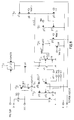
- FIG 6 A second embodiment of the bit cell circuit, together with drivers for the bit cell wires d, d* and acc, is shown in FIG 6. Elements corresponding to elements in FIG 5 have got the same references.
- the bit cell 7′ is shown surrounded by dashed lines.
- the load is the source/drain path of a MOS FET I1 and I2, respectively, shown to be of p-type in this embodiment, i.e. the opposite type of the type of the transistors T1 and T2 shown to be of n-type in this embodiment.
- the gate of the transistor I1 is connected to the node n2, and the gate of the transistor I2 is connected to the node n1.
- the bit cell can store a value v store , the value being either 'true' or 'false'.
- the bit cell has a structure such that it is settable in several different functional states by setting different potentials on the wires acc, d and d*.
- the control states are high level, low level, current into cell for all the wires and also current out of cell for the wire acc.
- the wire acc is an access wire going from the head 8 and connected to all the bit cells 7 in a storage element.
- the third and fourth wires d and d* have signals inverted to each other when writing or reading of the cells is made and the access wire acc is LOW.
- the driver and sense amplifiers in the head 8 is illustrated schematically in a dashed square in FIG 6.
- the control of the access wire acc is made in the head 8, which in turn is controlled from the external central control unit, which provides the voltages Vr and V3, and also a precharge signal prech.
- a first transistor T3, in this embodiment shown as being of n-type, has its source connected to a voltage Vr, its drain to the access wire acc in all the bit cells 7′ in a storage cell and its gate is fed with the precharge signal prech, which could be regarded as a clock signal.
- a second transistor T4 in this embodiment shown as being of n-type, has its source connected to a voltage 0V, its drain to the access wire acc in all the bit cells 7′ in a storage cell and its gate is controlled by an external control, which sets a voltage V3 which will be high when the voltage 0V shall be set on the access wire acc.
- the wire acc will be connected to all the bit cells in a storage cell, and all the bit cells will thus have the same control regarding the wire acc.
- a precharge is made in a first phase, controlling the MOS FET T3 to its conducting state and thus setting the wire acc on the voltage Vr.
- the signal V3 being either high or low depending upon the kind of control to be made, low or high voltage for the wire acc, is fed to the MOS FET T4.
- the voltage level of the wire acc is amplified in an amplifier AMP and transferred to the external circuits for further operation.
- FIG 8 An embodiment of the whole element head is shown in FIG 8 and will be described further below.
- the provision of the control signals to the head 8, as well as to the driver and sense circuit 9 described below, is not a part of this invention and will therefore not be further described.
- FIG. 6 An embodiment of a drive and sense circuit 9 for the bit cell wires d and d* is illustrated schematically in another dashed square in FIG 6. However, it is to be noted that the circuit 9 only illustrates one possible way to drive and sense the wires d and d*.
- the input/output IN/OUT is connected to the core cell 3 shown in FIG 1.
- the circuit 9 is one of many similar circuits that could be provided in an interface between the object storage 1 and the core cell 3.
- the write circuit for the wire d includes a first pair of transistors T5 and T6, the first shown to be of n-type and the second of p-type in the embodiment, having their drains connected to the wire d, and providing a voltage divider.
- the transistor T5 has its source connected to a potential Vr, and its gate is fed with the precharge signal prech.
- the other transistor T6 has its source connected to a potential Vcc, and its gate is fed with a control signal V4 going low when the potential Vcc shall be fed to the wire d as will be explained further below.
- the write circuit for the wire d also includes a series connection of the source/drain paths of a p-type transistor T9 and a n-type transistor T10 connected between the voltage source Vcc and the drain of a n-type transistor T11 having its source connected to ground and its gate connected to an input write from the external control.
- the interconnection between the drains of the transistors T9 and T10 is connected to the gate of the transistor T6 and bears the voltage V4.
- the gate of the transistor T9 is fed with the inverted precharge signal prech* connecting the gate of the transistor T6 to the source voltage Vcc through a conducting transistor T9 during the precharge phase.
- the write circuit for the wire d* includes a second pair of series coupled transistors T7 and T8, the first shown to be of n-type and the second of p-type in the embodiment, having their drains connected to the wire d*, and also providing a voltage divider.
- the transistor T7 has its source connected to a potential Vr, and its gate is fed with the precharge signal prech.
- the other transistor T8 has its drain connected to a potential Vcc, and its gate is fed with a control signal V5 going low when the potential Vcc shall be fed to the wire d*.
- the write circuit for the wire d* also includes a series connection of the source/drain paths of a p-type transistor T12 and a n-type transistor T13 connected between the voltage source Vcc and the drain of the transistor T11.
- the interconnection between the drains of the transistors T12 and T13 is connected to the gate of the transistor T8 and bears the voltage V5.
- the gate of the transistor T12 is fed with the inverted precharge signal prech* connecting the gate of the transistor T8 to the source voltage Vcc through a conducting transistor T12 during the precharge phase.
- the external wire IN/OUT for input and output is connected to two tristate inverters.
- One of the tristate inverters having its output connected to the wire IN/OUT includes a series connection of the source/drain paths of two n-type transistors T14, T15 and two p-type transistors T16, T17.
- the gate of the transistor T16 is connected to an external control wire providing the signal bitin and the gate of the transistor T15 is fed with the inverted signal bitin*.
- the second of the tristate inverters having its input connected to the wire IN/OUT includes a series connection of the source/drain paths of two n-type transistors T18, T19 and two p-type transistors T20, T21.
- the gate of the transistor T19 is connected to the external control wire providing the signal bitin and the gate of the transistor T20 is fed with the inverted signal bitin*.
- the output of the second tristate inverter is connected to the gate of the transistor T13 and through an inverter INV to the gate of the transistor T10.
- a read amplifier including a n-type transistor T22 having its source connected to earth, its gate connected to a constant voltage Vbias which holds the transistor T22 constantly conducting and functioning as a current generator, and its drain connected to a parallel connection of two series connected source/drain paths of a n-type transistor and a p-type transistor, T23, T24 and T25, T26, respectively, having their other end connected to the source voltage Vcc.
- the gates of the p-type transistors T24 and T25 are interconnected and connected to the interconnection of the drains of the transistors T23 and T24.
- the gate of the transistor T23 is connected to the wire d of the bit cell 7′, and the gate of the transistor T25 is connected to the wire d*.
- each clock period, the signals prech and prech*, is divided into a precharge phase, in which the signal prech is high, and a make phase, in which the signal prech is low and the other control signals from the external control determines the operation to be made.
- the precharge phase the wires d, d* and acc are precharged to the voltage Vr, through the transistors T5, T7 and T3, respectively.
- the signals bitin and bitin* controls when data will be sent to and from the bit cell 7′. When the signal bitin is low and the signal bitin* high, then data will be transferred from the bit cell to the wire IN/OUT by the first tristate inverter. When the signal bitin is high and the signal bitin* low, then data will be transferred to the bit cell from the wire IN/OUT by the second tristate inverter.
- the wires d and d* are left floating, and the wire acc is set to the voltage 0V by a high voltage V3 making the transistor T4 conducting.
- V3 makes the transistor T4 conducting.
- This causes the node having the lowest potential, say n1, to be lowered to a potential between Vr and 0V.
- n1 the node having the lowest potential
- This current discharges the the wire d, i.e. the voltage on the wire d is lowered. This voltage reduction is measured by the read amplifier T22 to T26.
- the result of the reading is provided on the interconnection between the drains of the transistors T25 and T26 and fed to the input of the first tristate inverter T14 to T17.
- the signal bitin being low and the signal bitin* being high provides a transfer of the read and amplified bit value to the input/output wire IN/OUT. It is important that the wires d and d* are not driven in an active way during the phase two, since then no voltage reduction should be obtained on one of the wires.
- both d and d* are initially provided on the potential Vr. Both d and d* are substantially kept on the potential Vr, but one of them falls somewhat because of "current in” into the cell which decharges one of the wires d, d*. Since Vr here is defined as “low”, the low potential will be lower than "low”. d and d* give the read values. d lower than d* gives FALSE, d higher than d* TRUE. For the don't write, write false, write true, don't write and don't comp. operations the information potentials on the wires d and d* don't give any information.
- the wire acc is set to the voltage 0V by a high voltage V3 making the transistor T4 conducting.
- the value to be stored is provided on the input/output wire IN/OUT.
- the signals bitin high and bitin* low activate the second tristate inverter T18 to T21 to transfer the value on the wire IN/OUT to its output.
- the control signal write being high on the gate of the transistor T11 connects the sources of the transistors T10 and T13 to 0V.
- the inverted signal from the second tristate inverter fed to the gate of the transistor T10, being low, will keep it non-conducting, the voltage V4 being connected to the voltage source Vcc during the precharge phase will be kept on this voltage.
- the transistor T6 will be kept non-conducting, and the voltage Vr connected to the wire d during the precharge interval through the transistor T5 will be kept.
- a low signal from the second tristate inverter T18 to T21, i.e. a "1" or true to be written, will control the write circuit T5, T6, T9, T10 for the wire d to set it on the high voltage Vcc through the inverter INV while the write circuit T7, T8, T12, T13 will keep the wire d* on the voltage Vr it was set on during the precharge phase.
- the storage nodes n1 and n2 are in the embodiment shown in FIG 6 used in the following way of operation.
- One of the nodes n1, n2 or both are charged or discharged during the second phase of the operation cycle dependent upon which ones of the control signals V3, V4 and V5 to be used, i.e. if the wire acc is set on 0V or if one of (or both) the wires d and d* is set on Vcc.
- every operation cycle is composed of a precharging period and an execution period.
- the wire acc is set high it is meant that the signal V3 is not controlling the transistor T4 to set the voltage 0V on the wire acc during the execution period.
- the wire d or d* is set low it is meant that the control signal V4 or V5 is not controlling the transistor T6 or T8 to be in a state coupling through the voltage Vcc, being higher than the voltage Vr, to the wire d or d* during the execution period.
- the wire d or d* is set high then the transistor T6 or T8 will be controlled to connect through the voltage Vcc to the wire.
- the storage cell area could be rather extensive, for instance including 256 storage cells, which means that each pair of transistors T5, T6 and T7, T8, respectively, is connected to a wire serving one bit cell in all the storage cells, such as 256 bit cells. Therefore, the transistor sizes must be adjusted to the total bus capacitances and the desired speed.
- the voltage Vr could be created from a shorted inverter in order to keep a known relation between Vr and the sense amplifier inverter.
- the access circuits in the head shall control the bit cells and also capture the information from the bit cells.
- control states are settable by the control states:
- the wire acc (access wire) gives the result of the comparison.
- the wire acc is precharged to Vr and the input data is supplied on the wire d, and its inverse value on the wire d*. If the value stored in the bit cell is different than the input data, the wire acc will be charged through one of the diodes D1 or D2, and through the corresponding n-type transistor, T1 or T2. This is detected by the amplifier AMP in the head 8. When a compared FIT is detected the wire acc will be kept on the potential Vr.
- the expressions current in and current out expresses that a charge is moved into and out of, respectively, the wire in question during a time sequence. This is usually made by initiating the wire to HIGH or LOW,respectively, in the operation mode REST and then change into the actual mode. A current will then discharge or charge, respectively, the wire in question. When there is no current no appreciable charge will be transported. Therefore, no voltage change will be provided during the time sequence.
- each 4-block has one pair of left hand side wires granta and reqa and four pair of right hand side wires req0, grant0,... to ... req3, grant3.
- a first 4-block 20 has its four pairs of right hand side wires connected to each of the pair of left hand side wires of four 4-blocks, of which the outer ones 21 and 22 are shown.
- the blocks 20, 21, and the blocks 20, 22 are interconnected with inverting amplifiers 23 and 24, the amplifier 23 giving information to a block lower in the block chain that a priority require is needed for a block higher in the clain, and the amplifier 24 giving information to a block higher in the block chain that a grant is given.
- the number of blocks 21,..22 in the second 4-block column are thus four.
- Each block in the second column is then connected to four 4-blocks in the third column of blocks in the same way as the blocks in the second column are connected to the 4-block 20.
- the number of 4-blocks in the third column will then be sixteen. Only the outermost 4-blocks 25 and 26 are shown.
- Each block in the third column is then connected to four 4-blocks in the fourth column of blocks in the same way.
- the number of 4-blocks in the third column will then be sixtyfour. Only the outermost 4-blocks 27 and 28 are shown.
- the right hand side wires of the 4-blocks in the fourth column are connected to the object storage. Each pair being adapted to serve as the buses 12 and 13 for a storage cell 1, as apparent from FIG. 7B.
- Eightyfive blocks are provided to serve 256 closures.
- the lowest block 28 is serving the lowest storage cells, down to the storage cell number 0, and the highest block 27 is serving the highest, i.e. up to the storage cell number 255.
- FIGs 7A and 7B uses a domino precharged logic, where the full priority decoder includes cascaded domino stages, corresponding to a transfer of a request signal from for instance req0 in the lowest block 28, through all priority decoder blocks and back to give a false grant signal to all storage cells, except the storage cell number 0.
- each block includes 5 rows of MOS FET transistors, each row including one MOS FET more than the row below, except for the fifth row which has the same number of MOS FET as the fourth row.
- Each of the MOS FETs Tr 0,0 to Tr 3,0 most to the right in the four lowest rows is shown to be of p-type having its gate connected to a clock signal source, its drain connected to a positive supply voltage and its source connected to the grant wire grant0, grant1, grant2 or grant3, respectively.
- the MOS FET Tr 4,0 in the highest row has its source, instead of being connected to a wire granti, i being a number between 0 and 3, connected to a wire reqa connected to the next lower block in the block cascade through an inverter 23.
- Tr 0,1 in the first row Tr 1,1 and Tr 1,2 in the second row
- Tr 2,1 , Tr 2,2 and Tr 2,3 in the third row
- Tr 3,1 , Tr 3,2 , Tr 3,3 and Tr 3,4 in the fourth row Tr 4,2 , Tr 4,3 , Tr 4,4 and Tr 4,5 in the fifth row
- Tr 4,2 , Tr 4,3 , Tr 4,4 and Tr 4,5 in the fifth row have their sources connected to earth and their drains connected to a grant wire grant0, grant1, grant2, or grant3, respectively, for the four lowest rows and to the wire reqa for the fifth row.
- the wire granta is connected to the gate of each of the MOS FETs Tr 0,1 , Tr 1,1 , each Tr 2,1 , Tr 3,1 .
- the wire req0 is connected to the gate of each of the MOS FETs Tr 1,2 , Tr 2,2 , Tr 3,2 and Tr 4,2 .
- the wire req1 is connected to the gate of each of the MOS FETs Tr 2,3 , Tr 3,3 and Tr 4,3 .
- the wire req2 is connected to the gate of each of the MOS FETs Tr 3,4 and Tr 4,4 .
- the wire req3 is connected to the gate of the MOS FET Tr 4,5 .
- the priority decoder operates in two phases. In the first phase, when the clock signal is low, all granti are precharged to be high (true). Then all the signals reqi will be low (no need). In the second phase the precharge is closed, i.e. the clock signal will be high. Then any or some of the outputs reqi will go high, which sets all the granti above to low (not chosen) and sets reqa to low. If a reqa goes low, then a reqi in a neighbouring 4-block to the left in FIG 7 is set to high. The signals reqa and granta in the 4-block 20 are of no importance. However, grant_a in the 4-block 20 is connected to earth. The signal reqa in the 4-block 20 provides the result "ANY" on the wire 14 in FIGs 1 and 2, since it has to go low when any reqi connected to any of the cell closures goes high.
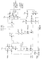
- FIG 8. A detail embodiment of the element head 8 is shown in FIG 8. This embodiment is adapted to the application of the object storage in a reduction kind of processor.
- the element head 8 controls the addess wire acc to the storage cells 7, it senses the access wire acc and wire ANY 14, here called any_type, it performs the operations wired_and and wired_nor on the buses a and b , and it also reads the buses a and b . Furthermore, it includes an internal dynamic memory bit.
- a n-channel MOS FET n0 has its source/drain path connected between a voltage Vr, being the same as the voltage Vr in FIG 6, and the access wire acc.
- a clock pulse cpb is fed to the gate of the MOS FET n0.
- a n-channel MOS FET n1 has its source/drain path connected between earth and the access wire acc.
- a series connection of the parallel coupled source/drain paths of two p-channel MOS FETs p2 and p3, the source/drain path of a p-channel MOS FET p4, and the drain/source path of a n-channel MOS FET n5 is connected between a voltage source Vcc and earth.
- a wire any_type directly connected to the nearest bit cell is connected to the gate of the MOS FET p2.
- a wire match from the central control unit (not shown) is connected to the gate of the MOS FET p3.
- the access wire acc is via an inverter INV 1 including the series connected source/drain paths of a p-channel MOS FET p1 and a n-channel n6 having their gates connected to the access wire acc. connected to the gate of the MOS FET p4.
- a n-channel MOS FET n7 has its source/drain path connected between the inverter INV1 and earth.
- a wire eval.s, i.e. evaluate select, from the central control unit is connected to the gate of the MOS FET n7.
- a wire set.s, i.e. set select, from the central control unit is connected to the gate of the MOS FET n5.
- the interconnection point i1 also called the select node, between the drains of the MOS FETs p4 and n5 is connected to the drain of a p-channel MOS FET p6, having its source connected via the drain/source path of a p-channel MOS FET p7 to the voltage source +Vcc.
- a wire reset.b from the central control unit is connected to the gate of the MOS FET p6.
- a wire b which is the same as the wire b shown in FIG 2, is connected to the gate of the MOS FET p7.
- a p-channel MOS FET p8 has its drain connected to a wire a , which is the same as the wire a shown in FIG 2, and its source to an interconnection point i2.
- a wire Wand.a i.e. wired and a , from the central control unit is connected to its inverted gate.
- a p-channel MOS FET p9 has its drain connected to the wire b , and its source to the interconnection point i2.
- a wire Wand.b, i.e. wired_and_ b from the central control unit is connected to its inverted gate.
- a p-channel MOS FET p10 has its drain connected to the interconnection point i2 and its source connected to the source voltage +Vcc.
- the interconnection point i1 is via and inverter INV2 connected to the inverted gate of the MOS FET p10.
- the inverter INV2 includes the series connected source/drain paths of a p-channel MOS FET p14 and a n-channel MOS FET n8 connected between the voltage source +Vcc and earth and having their gates connected to the interconnection point i1.
- a series connection of the drain/source paths of two p-channel MOS FETs p11 and p12 is connected between the wire a and the voltage source +Vcc.
- a wire Wor i.e. wired or, from the central control unit is connected to the gate of the MOS FET p12.
- the interconnection point i1 is connected to the gate of the MOS FET p11.
- a p-channel MOS FET p13 has its source/drain path connected between the wire a and the interconnection point i1.
- a wire s.a, i.e. select a from the central control unit is connected to the gate of the MOS FET p13.
- a series connection of the drain/source paths of a n-channel MOS FET n2, a p-channel MOS FET p15, a p-channel MOS FET p16 is connected between earth and the voltage source +Vcc.
- An interconnection point i3 between the sources of the MOS FETs n2 and p15 is connected to the gate of the MOS FET n1.
- a series connection of two p-channel MOS FETs p17 and p18 is connected between the interconnection point i3 and the voltage source +Vcc.
- the interconnection point i1, the select node, is connected to the gate of the MOS FET 18.
- read/write b from the central control unit is connected to the inverted gate of the MOS FET p15.
- the function of the logic in the embodiment of the element head shown in FIG 8 is the following.
- the MOS FET n0 precharges the access wire acc at each negative clock pulse, and the MOS FET n1 evaluates it low at read or write.
- the MOS FET n2 precharges i3 low to keep the MOS FET n1 off, i.e. non-conducting, at stand-by.
- the MOS FETs p17 and p18 perform read/write controlled by the select node. This is used for instance in instructions of type instruction match, clearing the mark of a closure cell or reading the identity of the closure cell and if not setting a mark, where different actions shall take place depending on the information on the buses a and b .
- a match function compares a value, for instance a so called goal value, in the core cell and in a storage cell and consider these values defining two sets. The match result is false if the sets do not intersect. This case is also assumed if parts of the closure are not fully evaluated.
- the MOS FET n5 precharges the select node i1, and the MOS FETs p2 to p4 evaluate it at control from the external control unit on the gate of the MOS FET n7.
- the MOS FETs p8 to p10 perform wired-and on the bus a and/or on the bus b in dependence of the control signals from the central control unit.
- the MOS FETs p11 and p12 perform wired_or on the bus a at control from the central control unit.
- the inverter INV2 inverts the select bit on the select node. This is necessary because both wired-or and wired-and are performed.
- the MOS FET p13 transfers the value on the bus a to the select node. Only a high state need be transferred, since it has been precharged to a low state. Finally, the MOS FETs p6 and p7 are used to select high when controlled. This is needed for an instruction for reading a marked storage cell and clearing the mark of that cell, because then the select node shall be reset at the same time as a reading is performed. This feature could also be used for other types of instructions in which a logical AND operation must be performed in the element head.
- the signal any_type is directly connected to the nearest bit cell. It contains the type of the stored value. During a match the MOS FET p3 is controlled to be off, so a high value on the wire having the signal any_type will generate a true match. Similarly, for a test of whether the storage cell is unused, a high state on the wire having the signal any_type while the MOS FET p3 is contolled to be off will cause the signal select on the select node to remain low. For a test regarding equality the MOS FET p3 is controlled to be on, i.e. conducting.
- the embodiment of a closure head 11 shown in FIG 9 is able to perform the priority operation and the MODE operation on either the bus a or the bus b . Also this embodiment is adapted to cooperation with a reduction type of computer. Both operations can be performed simultaneously on different buses.
- the MODE operation i.e. the operation of the bus 4 (MODE) in the circuit shown in FIGs 1 and 2, is sensitive to either high or low states on the bus a , while it is sensitive only to the low state on the bus b .
- the closure head can also reset the global signal MORE on the bus 5 (see FIG. 1), and read and write back old bus data to the buses a and b .
- Both the circuit to perform the MODE operation and the circuit to perform the priority operation are designed according to a two stage domino principle.
- the first stage determines which bus should be the input and correct the polarity, and the second stage performs the actual operation.
- the closure head operates in two phases, having a first precharge phase, and a second operation phase. Therefore, a number of precharge n-channel MOS FETs n20, n21, n22 and n23 are provided having their gate controlled by a clock signal prech from the central control unit.
- n20 precharges the bus a , n21 the bus b , n22 the bus req to the priority decoder 2 and n23 a contact net F1 to "low".
- a contact net F1 includes two parallel coupled series coupled pairs of source/drain paths of p-channel MOS FETs p20, p21 and p22, p23, respectively.
- the net F1 is on one hand connected to earth through the source/drain path of the MOS FET n23 and on the other hand to the voltage source +Vcc.
- the bus a is connected to the gate of the MOS FET p20 and through an inverter INV 20 to the gate of the MOS FET p23, which thus is fed with the signal a* being the inverted signal a on the bus a .
- a signal mode.a from the central control unit is fed to the gate of the MOS FET p21 and its inverted signal mode.
- a* from the central control unit is fed to the gate of the MOS FET p22.
- the contact net F1 realizes the function a*mode.a versus a**mode.a*.
- a series connection of the source/drain paths of two p-channel MOS FETs p24 and p25 are connected between the voltage source +Vcc and the bus b .
- the bus a is connected to the gate of the MOS FET p24 and a signal ba from the central control unit is fed to the gate of the MOS FET p25.
- the node between the net F1 and the drain of the MOS FET n23 is connected to the gate of a n-channel MOS FET n24 having its source connected to earth and its drain to the bus 4 (MODE) shown in FIGs 1 and 2 providing the mode-signal.
- MODE bus 4
- a series connection of the source/drain paths of two p-channel MOS FETs p26 and p27 are connected between the voltage source +Vcc and the bus b .
- the mode-signal on the bus 4 is also through two inverters INV 21 and INV 22, amplifying the mode-signal, connected to the gate of the MOS FET p27.
- a signal mode.b is fed from the central control unit to the gate of the MOS FET p26.
- the signal mode.a makes the mode operation on the bus a.
- the signal mode.a* makes also the mode operation on the bus a but forms an inverted value a* on the bus.
- the signal ba set the bus “high” if the bus a is set “low”.
- the signal mode.b sets bus b to "high” if the bus mode is “low”.
- the signal prech is used to precharge the buses a and b to "low".
- the selection of if the MODE operation is to be made on the signal a or the signal a* is made by aid of the contact net F1.
- the bus MODE 4 may then be set to earth right through all the closure heads 11 in the object storage.
- a control signal mode.b on the gate of the transistor p26 will then draw the bus b to a high level. In this way it is possible to make two different tests, on the bus a as well as on the bus b . If the test on the bus a shows a result "high” conditioned in the actual operation, then the bus b may be set "high".
- WIRED OR may be made on one of the buses a and b and WIRED AND on the other, and a logical operation may be made in which the condition could be that if the result on the bus a is for instance "false” then the bus b could show "false". Another condition is to make another operation based on the result on the bus b .
- a series connection of the source/drain paths of two p-channel MOS FETs p28 and p29 are connected between the voltage source +Vcc and the bus b .
- the signal grant from the priority decoder 2 is through an inverter INV 23 connected to one input of a NAND gate NAND1 and the signal req to its second input.
- the NAND gate includes two n-channel MOS FETs 25 and 26 having their source/drain paths series connected and two p-channel MOS FETs p32 and p34 having their source/drain paths parallel connected and connected between the drain of the MOS FET n26 and the source voltage Vcc.
- the source of the MOS FET n25 is connected to earth.
- the signal grant* is fed to the gates of the MOS FETs n26 and p34 and the signal req is fed to the gates of the MOS FETs n25 and p32.
- the output of the NAND gate is connected to the gate of the MOS FET p28 and to the gate of a p-channel MOS FET p33 having its source/drain path connected between the source voltage Vcc and the wire MORE 5.
- a signal grant.b from the central control unit is fed to the gate of the MOS FET p29.
- a series connection of the source/drain paths of two p-channel MOS FETs p30 and p31 are connected between the voltage source +Vcc and the bus req to the priority decoder 2.
- a signal prio from the central control unit is fed to the gate of the MOS FET p30, and the bus b is connected to the gate of the MOS FET p31.
- the signal prio from the central control unit is used to send a request signal to the priority decoder 2, i.e. provide a high signal req, if the bus b is "low".
- the NAND-gate p32, p34, n25, n26 feels if the signal req is high and the signal grant is low, i.e. if a need for priority is demanded but not chosen. In such a case the NAND-gate goes low and sets the bus 5 (MORE) on "high", i.e. indicating that there is a need for priority.
- the signal grant.b is used in order to set the bus b "high” if the signal req is "high” and the signal grant is "low". After that first a signal prio has been provided from the central control unit and then a signal grant.b at the most one storage cell in the object storage will have a bus b being "low".
Landscapes
- Engineering & Computer Science (AREA)
- Software Systems (AREA)
- Theoretical Computer Science (AREA)
- Physics & Mathematics (AREA)
- General Physics & Mathematics (AREA)
- General Engineering & Computer Science (AREA)
- Computing Systems (AREA)
- Computational Mathematics (AREA)
- Mathematical Optimization (AREA)
- Pure & Applied Mathematics (AREA)
- Mathematical Analysis (AREA)
- Computer Hardware Design (AREA)
- Microelectronics & Electronic Packaging (AREA)
- Nonlinear Science (AREA)
- Devices For Executing Special Programs (AREA)
- Stored Programmes (AREA)
- Static Random-Access Memory (AREA)
- Complex Calculations (AREA)
- Executing Machine-Instructions (AREA)
- Saccharide Compounds (AREA)
- Multi Processors (AREA)
- Information Retrieval, Db Structures And Fs Structures Therefor (AREA)
- Hardware Redundancy (AREA)
- Exchange Systems With Centralized Control (AREA)
- Advance Control (AREA)
- Vehicle Body Suspensions (AREA)
- Memory System (AREA)
- Medicines That Contain Protein Lipid Enzymes And Other Medicines (AREA)
- Monitoring And Testing Of Nuclear Reactors (AREA)
- Semiconductor Memories (AREA)
- Memory System Of A Hierarchy Structure (AREA)
- Measuring Pulse, Heart Rate, Blood Pressure Or Blood Flow (AREA)
- Mobile Radio Communication Systems (AREA)
- Pharmaceuticals Containing Other Organic And Inorganic Compounds (AREA)
- Control Of Indicators Other Than Cathode Ray Tubes (AREA)
- Studio Devices (AREA)
- Controls And Circuits For Display Device (AREA)
- Transforming Electric Information Into Light Information (AREA)
- Paper (AREA)
- Steering Control In Accordance With Driving Conditions (AREA)
Claims (24)
- Une mémoire associative ayant une structure de bus de mémoire (t1, t2, id, env, v0, v1, v2, v3) pour des données, comprenant :
plusieurs cellules de mémoire (1), chacune pour l'enregistrement d'une information composée et couplée à une structure de bus de mémoire pour des données,
des moyens pour effectuer des opérations de recherche par la structure de bus de mémoire pour des données clés parmi les cellules pour établir au moins un état de sélection ou de non-sélection pour la cellule de mémoire,
un (des) moyen(s) de tête (8) dans chacune des cellules de mémoire pour l'enregistrement de la marque ou des marques,
un décodeur à priorité (2) auquel toutes les cellules de mémoires sont couplées et qui sélectionne une cellule parmi plusieurs pour des opérations demandant la sélection d'une cellule de mémoire individuelle,
un moyen (11) dans chaque cellule de mémoire pour établir un état de demande prioritaire, parmi les cellules de mémoires objets basé sur une ou plusieurs marques dans lesdits moyens principaux dans la cellule de mémoire actuelle pour une opération réelle qui doit être faite, si l'opération en question demande la sélection d'une cellule de mémoire individuelle, et,
une première structure de bus de contrôle (any-type, Vr, cpb, set.s, match, r/w.s, r/w.b, r/w.r, Wand.a, Wand.b, Wor, s.a., reset.b, mode.a, mode.a*, prech, ba, mode.b, grant.b, prio etc) pour la commande externe de ces cellules de mémoires objets qui ont leurs marques mises simultanément, en accord avec une commande pour l'opération réelle et couplées pour contrôler les moyens (11) en fixant l'état de demande prioritaire, d'établir l'état de demande quand celui-ci est demandé et caractérisée en ce que le décodeur à priorité (2) comprend un circuit qui lit l'état de demande des moyens (11) et qui met l'état de demande prioritaire dans toutes les cellules de mémoire, en sélectionnant une des cellules de mémoire qui fait la demande, et qui, ainsi, ayant la marque "établie" pour l'indication de l'état de sélection et donnant un résultat individuel pour chaque cellule de mémoire dans la mémoire indiquant la sélection ou non-sélection de la cellule en question. - Une mémoire selon la revendication 1, caractérisée en ce que le décodeur à priorité (2) comprend un circuit combinaison (20 à 27) indiquant un état de demande prioritaire de toutes les cellules de mémoire et renvoyant un signal à toutes les cellules de mémoire indiquant en même temps la sélection ou non-sélection.
- Une mémoire selon l'une quelconque des revendications 1 à 2, caractérisée en ce que le décodeur à priorité (2) comprend une section pour chaque cellule de mémoire, chaque section ayant une première connexion "DEMANDE", sur laquelle un bit de valeur "vrai" représente un besoin de sélection de la cellule de mémoire et un bit de valeur "faux" ne répresente aucun besoin de sélection de la cellule de mémoire, et une deuxième connexion pour la sélection reçue de la cellule de mémoire, sur laquelle un bit de valeur "vrai" représente choisi et "faux" non choisi.
- Une mémoire selon l'une quelconque des revendications 1 à 3, caractérisée en ce que chaque cellule de mémoire contient un certain nombre de champs de mémoire (IDENTITY, ENVIRONMENT, VALUE/DES.₀, VALUE/DES.₁, VALUE/DES₂, VALUE/DES.₃), chacun contenant un (des) moyen(s) de tête des champs de mémoire (8), chacun étant adapté pour la mémorisation de la marque,
les moyens de tête des champs de mémoire (8) dans une cellule de mémoire étant interconnectés, des moyens étant établis pour au moins une opération logique connectée des états de marque "établie" dans les moyens de tête,
le moyen (11) pour l'établissement de la demande est alimenté du résultat des opérations logiques, se basant ainsi sur un calcul effectué à l'intérieur de la mémoire, et établit l'état de demande prioritaire dépendant du résultat des opérations connectées logiques et dépendant des signaux externes de contrôle indiquant la nature de l'opération logique connectée nécessaire lors de l'opération particulière momentanée de la mémoire,
les moyens pour effectuer des opérations de recherche comprennent un dispositif dans chaque champ de mémoire pour indiquer la comparaison entre une valeur externe sur le dispositif de bus des données et au moins une partie choisie du contenu du champ de mémoire et l'alimentation du bit de marque dépendant du résultat de la comparaison. - Une mémoire selon l'une quelconque des revendications 1 à 4, caractérisée en ce que au moins un bus global (4, 5, 14) est établi, connecté à chacune des cellules de mémoire pour l'indication d'une opération logique du type "ET" ou "OU", et des moyens (11) dans chaque cellule de mémoire comprenant au moins une porte logique connectée à au moins un bus global afin de contrôler la cellule de mémoire de prendre part d'une opération logique réelle selon une condition établie par le contrôle externe de la (des) porte(s).
- Une mémoire selon l'une quelconque des revendications 1 à 5, caractérisée en ce que chaque cellule de mémoire contient au moins un champ de mémoire d'état (LAZY, WHERE, TYPE), indiquant l'état ou les états du contenu de la cellule de mémoire.
- Une mémoire selon l'une quelconque des revendications 1 à 6, caractérisée en ce que chaque cellule de mémoire est divisée en un nombre de champs de mémoire (IDENTITY, ENVIRONMENT, VALUE/DES.₀, VALUE/DES.₁, VALUE/DES₂, VALUE/DES.₃), chacun contenant un moyen de tête des champs de mémoire (8), chacun étant adapté pour la mémorisation de la marque, et que, au moins un deuxième bus (a, b) est connecté au moyen de tête (8) dans les champs de mémoire (6) dans chaque cellule de mémoire pour indiquer des opérations logiques du type "CONNECTEE ET" et "CONNECTEE OU" entre les champs de mémoire, chacun des champs de mémoire comprenant des moyens pour la lecture d'au moins le deuxième bus et de prendre part d'une opération logique réelle.
- Une mémoire selon l'une quelconque des revendications 1 à 7, caractérisée en ce que les cellules de mémoires sont connectées à une unité de côntrole centrale par laquelle le dispositif de bus de contrôle qui est transmis aux cellules de mémoire et aux moyens de contrôles pour les cellules de mémoire, des mots de données étant capables d'être transférés à la ou de la mémoire sur le dispositif de bus connecté à des moyens des données d'entrée ou de sortie (9) par une information composée comprise sur le dispositif de bus.
- Une mémoire selon l'une quelconque des revendications 4 à 8, caractérisée en ce que chaque champ de mémoire comprend un des moyens de tête (8) mémorisant les marques, sous la forme d'étiquettes, et un nombre de cellules de bit dans lesquelles les bits de mots des données sont mémorisés, chaque cellule étant connectée à chacune des autres cellules dans le même champ de mémoire et au moyen de tête.
- Une mémoire selon la revendication 9, caractérisée en ce que le contrôle des cellules de bit du moyen de tête (8) dépend des conditions logiques chacune étant une fonction de données sur les deuxièmes bus (a, b), une (des) marque(s) étant présente(s) jusqu'au contrôle actuel, le résultat de la comparaison dans le cas de l'opération de comparaison et un signal de contrôle de l'unité de commande centrale à la mémoire.
- Une mémoire selon les revendications 8 et 9, caractérisée en ce que la (les) marque(s) étant sous la forme d'étiquette(s) est (sont) règlable(s) dépendant sur des conditions logiques, chacune étant une fonction de données sur les deuxièmes bus (a, b), une (des) marque(s) étant sous la forme d'étiquette(s) et présente(s) jusqu'au nouvel règlage, le résultat de la comparaison dans le cas de l'opération de comparaison et un signal de contrôle de l'unité de commande central à la mémoire.
- Une mémoire selon l'une quelconque des revendications 8 à 11, caractérisée en ce qu'un premier fil (acc) connecté au moyen de tête (8) interconnecte toutes les cellules de bit dans un champ de mémoire (6); en ce que toutes les cellules de bit dans la mémoire sont établies dans des rangées et des colonnes, les cellules de bit de chaque rangée étant incluses dans une individuelle parmi les cellules de mémoire; et en ce que toutes les cellules de bit dans le champ de mémoire (6) sont commandées par des signaux sur le premier fil (acc), et que, pour chaque colonne de cellule de bit dans la mémoire, d'autres fils (d, d*) sont connectés à toutes les cellules de bit dans la colonne de cellule de bit et connectés aux moyens des données d'entrée et de sortie (9).
- Une mémoire selon l'une quelconque des revendications 1 à 12, caractérisée en ce qu'une recherche est faite en faisant une comparaison de la (des) marque(s), étant sous la forme d'étiquette(s), par un contrôle des moyens de tête (8) dans les champs de mémoire et afin d'obtenir le résultat "la comparaison est correcte" ou "la comparaison n'est pas correcte", et que la recherche est faite d'une des façons suivantes :(1) recherche individuelle et indépendante de chaque champ de mémoire (6) de l'information composée dans d'autres champs de mémoire dans la mémoire, seul le moyen de tête (8) pour le champ de mémoire choisi individuellement étant contrôlé,(2) recherche en utilisant une comparaison pour la sélection des champs de mémoire (6) dans les cellules de mémoire, les moyens de tête (8) dans les champs sélectionnés étant contrôlés et le résultat étant "la comparaison est correcte" dans chaque champ de mémoire sélectionné dans les cellules de mémoires étant sélectionnées en concordance avec la condition de la recherche, et(3) recherche en utilisant une comparaison pour les champs sélectionnés dans une cellule de mémoire, les moyens de tête (8) dans les champs sélectionnés étant contrôlés et le résultat étant "la comparaison est correcte" dans au moins un des champs de mémoire sélectionnés, dans les cellules de mémoire étant sélectionnées en concordance avec la condition de la recherche.
- Une mémoire selon les revendications 4 et 13, caractérisée en ce que la comparaison pour un profil binaire dans le champs de mémoire à un profil binaire sur le dispositif de bus des données de mémoire est faite dans une des façons suivantes dépendantes du décodage des données à être comparées les unes aux autres, où chaque profil binaire peut être codé dans deux façons différentes :(1) si le profil binaire dans le champ de mémoire et le profil binaire sur le bus des données ont un premier type de codage, indicant une valeur d'information spécifique, une opération de comparaison ayant pour résultat que "la comparaison est correcte" uniquement quand tous les bits correspondants dans les deux profils binaires sont pareils.(2) si au moins un des profils binaires dans le champs de mémoire et le profil binaire sur le bus des données a un deuxième type de codage, indiquant une valeur d'information arbitraire, une opération de comparaison ayant toujours pour résultat que "la comparaison est correcte".
- Une mémoire selon l'une quelconque des revendications 1 à 14, caractérisée en ce qu'elle comprend des cellules de bit, chaque cellule de bit étant capable à mémoriser une valeur de bit, la valeur étant soit "vraie" ou "fausse", la cellule de bit comprenant :
une bascule comprenant une paire de transistors et des charges associées (T1, T2, L1, L2; T1, T2, I1, I2) en couplage croisé, la tension d'alimentation de la bascule étant présente entre la première connexion (vcc) et la seconde connexion (acc) et pouvant être commandée à partir de chaque côté par l'intermédiaire des troisième et quatrième connexions (d, d*), et ayant un premier et un second noeud (n1, n2) pouvant être placés à des niveaux de tension mutuellement différents, l'une des combinaisons de niveaux de tension indiquant un état de bit enregistré "vrai" et l'autre indiquant un état de bit enregistré "faux", et des premiers moyens de redressement séparés (D1) connectés entre la troisième connexion (d) et le premier noeud (n1), et des seconds moyens de redressement séparés (D2) connectés entre la quatrième connexion (d*) et le second noeud (n2);
le moyen des données d'entrée et de sortie (9) étant connecté aux troisième et quatrième connexion (d, d*);
le moyen de tête (8) étant connectés aux seconde connexions (acc); la première connexion étant constamment alimentée par une tension d'alimentation, la seconde, troisième et quatrième connexions peuvent prendre différents états établis, par l'action des moyens des données d'entrée et de sortie (9) et le moyen de tête (8), de façon que la cellule puisse prendre plusieurs états fonctionnels parmi un ensemble d'états fonctionnels, chacun d'eux étant représenté par une combinaison spécifique établie des seconde, troisième et quatrième connexions; et en ce que pour un état fonctionnel, dans le but de comparer l'état de la cellule avec des données d'entrée, le moyen des données d'entrée et de sortie (9) placent une paire de signaux d'entrée complémentaires sur les troisième et quatrième connexions (d, d*), et le moyen de tête (8) comprend des troisième moyens (T3) pour précharger la seconde connexion (acc) à un niveau de tension de référence (Vr) et des quatrième moyens (AMP) pour détecter un changement de tension sur la seconde connexion. - Une cellule de bit de mémoire selon la revendication 15, caractérisée en ce que les états établis pour les seconde, troisième et quatrième connexions du circuit de cellule sont : un niveau "haut", un niveau "bas", aucun courant n'entrant dans la cellule, un courant entrant dans la cellule pour les troisième et quatrième connexions et également un courant sortant de la cellule pour la seconde connexion (acc), les niveaux "haut" et "bas" étant liés au fait que les tensions sont considérées comme de sens positif ou de sens négatif, c'est-à-dire au fait que la tension (Vcc) sur la première connexion est positive ou négative par rapport à la masse.
- Une cellule de bit de mémoire selon les revendications 15 ou 16, caractérisée en ce que, pour tous les états fonctionnels du circuit de cellule, les moyens des données d'entrée et de sortie (9) et les moyens de tête (8), sont conçus pour commander les seconde, troisième et quatrième connexions (acc, d, d*) avec un cycle de commande comprenant deux phases, à savoir une première phase de précharge dans laquelle les seconde, troisième et quatrième connexions sont connectées de façon à recevoir une tension supplémentaire (Vr) comprise entre la tension de la première connexion (Vcc) et la masse, et une seconde phase de fonctionnement pour les placer dans un état fonctionnel désiré, un niveau "haut" et "bas" étant fixé en relation avec cette tension supplémentaire (Vr), et ce niveau "haut" ou "bas" étant lié au fait que les tensions dans le circuit sont considérées comme de sens positif ou de sens négatif.
- Une cellule de bit de mémoire selon l'une quelconque des revendications 16 ou 17, caractérisée en ce qu'un mode de fonctionnement "repos" est établi par les moyens des données d'entrée et de sortie (9) et les moyens de tête (8) en fixant la combinaison suivante sur les seconde, troisième et quatrième connexions (acc, d, d*) : haut, bas, bas.
- Une cellule de bit de mémoire selon l'une quelconque des revendications 16 à 18, caractérisée en ce qu'un mode de fonctionnement "lecture, faux" est établi par les moyens des données d'entrée et de sortie et les moyens de tête ayant la combinaison suivante sur les seconde, troisième et quatrième connexions (acc, d, d*) : bas, courant entrant, bas.
- Une cellule de bit de mémoire selon l'une quelconque des revendications 16 à 19, caractérisée en ce qu'un mode de fonctionnement "lecture vrai" est établi par les moyens des données d'entrée et de sortie et les moyens de tête ayant la combinaison suivante sur les seconde, troisième et quatrième connexions (acc, d, d*) : bas, bas, courant entrant.
- Une cellule de bit de mémoire selon l'une quelconque des revendications 16 à 20, caractérisée en ce qu'un mode de fonctionnement "pas de lecture et pas d'écriture" est établi par les moyens de tête (8) en fixant la seconde connexion (acc) au niveau haut.
- Une cellule de bit de mémoire selon l'une quelconque des revendications 16 à 21, caractérisée en ce que la seconde connexion est une connexion d'accès (acc), et en ce qu'au moment d'écriture dans le circuit de cellule les moyens des données d'entrée et de sortie placent une paire de signaux d'entrée complémentaires sur les troisième et quatrième connexions (d, d*) et en ce que les moyens de tête comprennent des cinquièmes moyens pour placer la seconde connexion (acc) à un niveau "bas".
- Une cellule de bit de mémoire selon l'une quelconque des revendications 16 à 22, caractérisée en ce que les moyens des données d'entrée et de sortie (9) sont conçus de façon à fixer des combinaisons différentes de signaux d'entrée sur les troisième et quatrième connexions (d, d*) pour les modes de fonctionnement "comp. faux" et "comp. vrai".
- Une cellule de bit de mémoire selon l'une quelconque des revendications 16 à 23, caractérisée en ce qu'un mode de fonctionnement "pas de comp." est établi par les moyens des données d'entrée et de sortie (9) en fixant à la fois les troisième et quatrième connexions (d, d*) au niveau bas, et en actionnant les troisième et quatrième moyens (T3 et AMP) dans le moyen de tête (8).
Applications Claiming Priority (3)
| Application Number | Priority Date | Filing Date | Title |
|---|---|---|---|
| SE9002558A SE9002558D0 (sv) | 1990-08-02 | 1990-08-02 | Processor |
| SE9002558 | 1990-08-02 | ||
| PCT/SE1991/000513 WO1992002932A1 (fr) | 1990-08-02 | 1991-08-01 | Memoire associative |
Publications (2)
| Publication Number | Publication Date |
|---|---|
| EP0541685A1 EP0541685A1 (fr) | 1993-05-19 |
| EP0541685B1 true EP0541685B1 (fr) | 1995-02-15 |
Family
ID=20380081
Family Applications (6)
| Application Number | Title | Priority Date | Filing Date |
|---|---|---|---|
| EP91914586A Expired - Lifetime EP0541683B1 (fr) | 1990-08-02 | 1991-08-01 | Processeur reductif |
| EP91914604A Expired - Lifetime EP0541685B1 (fr) | 1990-08-02 | 1991-08-01 | Memoire associative |
| EP91914592A Withdrawn EP0548094A1 (fr) | 1990-08-02 | 1991-08-01 | Unite active de memoire dans un processeur de reduction |
| EP91914583A Expired - Lifetime EP0541682B1 (fr) | 1990-08-02 | 1991-08-01 | Procede pour effectuer des operations arithmetiques logiques et apparentees et unite arithmetique numerique |
| EP91914521A Expired - Lifetime EP0541678B1 (fr) | 1990-08-02 | 1991-08-01 | Unite arithmetique pour arithmetique structurale |
| EP91914596A Expired - Lifetime EP0541684B1 (fr) | 1990-08-02 | 1991-08-01 | Cellule de memoire binaire |
Family Applications Before (1)
| Application Number | Title | Priority Date | Filing Date |
|---|---|---|---|
| EP91914586A Expired - Lifetime EP0541683B1 (fr) | 1990-08-02 | 1991-08-01 | Processeur reductif |
Family Applications After (4)
| Application Number | Title | Priority Date | Filing Date |
|---|---|---|---|
| EP91914592A Withdrawn EP0548094A1 (fr) | 1990-08-02 | 1991-08-01 | Unite active de memoire dans un processeur de reduction |
| EP91914583A Expired - Lifetime EP0541682B1 (fr) | 1990-08-02 | 1991-08-01 | Procede pour effectuer des operations arithmetiques logiques et apparentees et unite arithmetique numerique |
| EP91914521A Expired - Lifetime EP0541678B1 (fr) | 1990-08-02 | 1991-08-01 | Unite arithmetique pour arithmetique structurale |
| EP91914596A Expired - Lifetime EP0541684B1 (fr) | 1990-08-02 | 1991-08-01 | Cellule de memoire binaire |
Country Status (23)
| Country | Link |
|---|---|
| US (6) | US5239502A (fr) |
| EP (6) | EP0541683B1 (fr) |
| JP (6) | JPH05508725A (fr) |
| KR (1) | KR930701818A (fr) |
| CN (6) | CN1027198C (fr) |
| AT (5) | ATE116455T1 (fr) |
| AU (6) | AU654149B2 (fr) |
| BG (3) | BG97381A (fr) |
| CA (6) | CA2086592A1 (fr) |
| DE (5) | DE69101242T2 (fr) |
| ES (3) | ES2051129T3 (fr) |
| FI (3) | FI930433A7 (fr) |
| HU (3) | HUT63710A (fr) |
| IL (6) | IL99055A (fr) |
| LT (6) | LTIP385A (fr) |
| NO (3) | NO930302L (fr) |
| NZ (3) | NZ239242A (fr) |
| RO (1) | RO109487B1 (fr) |
| SE (1) | SE9002558D0 (fr) |
| SK (2) | SK402592A3 (fr) |
| TW (5) | TW215483B (fr) |
| WO (6) | WO1992002876A1 (fr) |
| ZA (6) | ZA916121B (fr) |
Families Citing this family (122)
| Publication number | Priority date | Publication date | Assignee | Title |
|---|---|---|---|---|
| WO1993024888A1 (fr) * | 1992-05-22 | 1993-12-09 | Massachusetts Institute Of Technology | Resolveur de reponse pour memoires associatives et processeurs paralleles |
| JP3376604B2 (ja) * | 1992-07-20 | 2003-02-10 | カシオ計算機株式会社 | 情報管理装置 |
| IT1270230B (it) | 1994-06-16 | 1997-04-29 | Enichem Sintesi | Composizione catalitica e processo per l'alchilazione di composti aromatici |
| US5619711A (en) * | 1994-06-29 | 1997-04-08 | Motorola, Inc. | Method and data processing system for arbitrary precision on numbers |
| GB2293468B (en) * | 1994-09-21 | 1999-09-29 | Sony Uk Ltd | Data processing systems |
| JP3037089B2 (ja) * | 1994-12-14 | 2000-04-24 | 川崎製鉄株式会社 | 連想メモリ |
| FR2736737B1 (fr) * | 1995-07-12 | 1997-08-14 | Alcatel Nv | Dispositif de gestion de relations entre des objets |
| US5943242A (en) * | 1995-11-17 | 1999-08-24 | Pact Gmbh | Dynamically reconfigurable data processing system |
| US7266725B2 (en) | 2001-09-03 | 2007-09-04 | Pact Xpp Technologies Ag | Method for debugging reconfigurable architectures |
| US6103579A (en) | 1996-01-31 | 2000-08-15 | Micron Technology, Inc. | Method of isolating a SRAM cell |
| US6750107B1 (en) * | 1996-01-31 | 2004-06-15 | Micron Technology, Inc. | Method and apparatus for isolating a SRAM cell |
| US5964825A (en) * | 1996-02-09 | 1999-10-12 | Texas Instruments Incorporated | Manipulation of boolean values and conditional operation in a microprocessor |
| US5706224A (en) * | 1996-10-10 | 1998-01-06 | Quality Semiconductor, Inc. | Content addressable memory and random access memory partition circuit |
| DE19651075A1 (de) | 1996-12-09 | 1998-06-10 | Pact Inf Tech Gmbh | Einheit zur Verarbeitung von numerischen und logischen Operationen, zum Einsatz in Prozessoren (CPU's), Mehrrechnersystemen, Datenflußprozessoren (DFP's), digitalen Signal Prozessoren (DSP's) oder dergleichen |
| DE19654593A1 (de) * | 1996-12-20 | 1998-07-02 | Pact Inf Tech Gmbh | Umkonfigurierungs-Verfahren für programmierbare Bausteine zur Laufzeit |
| DE19654595A1 (de) | 1996-12-20 | 1998-07-02 | Pact Inf Tech Gmbh | I0- und Speicherbussystem für DFPs sowie Bausteinen mit zwei- oder mehrdimensionaler programmierbaren Zellstrukturen |
| US6338106B1 (en) | 1996-12-20 | 2002-01-08 | Pact Gmbh | I/O and memory bus system for DFPS and units with two or multi-dimensional programmable cell architectures |
| ATE243390T1 (de) | 1996-12-27 | 2003-07-15 | Pact Inf Tech Gmbh | Verfahren zum selbständigen dynamischen umladen von datenflussprozessoren (dfps) sowie bausteinen mit zwei- oder mehrdimensionalen programmierbaren zellstrukturen (fpgas, dpgas, o.dgl.) |
| DE19654846A1 (de) * | 1996-12-27 | 1998-07-09 | Pact Inf Tech Gmbh | Verfahren zum selbständigen dynamischen Umladen von Datenflußprozessoren (DFPs) sowie Bausteinen mit zwei- oder mehrdimensionalen programmierbaren Zellstrukturen (FPGAs, DPGAs, o. dgl.) |
| US6374346B1 (en) | 1997-01-24 | 2002-04-16 | Texas Instruments Incorporated | Processor with conditional execution of every instruction |
| DE19704044A1 (de) * | 1997-02-04 | 1998-08-13 | Pact Inf Tech Gmbh | Verfahren zur automatischen Adressgenerierung von Bausteinen innerhalb Clustern aus einer Vielzahl dieser Bausteine |
| DE19704728A1 (de) | 1997-02-08 | 1998-08-13 | Pact Inf Tech Gmbh | Verfahren zur Selbstsynchronisation von konfigurierbaren Elementen eines programmierbaren Bausteines |
| US6542998B1 (en) | 1997-02-08 | 2003-04-01 | Pact Gmbh | Method of self-synchronization of configurable elements of a programmable module |
| DE19704742A1 (de) | 1997-02-11 | 1998-09-24 | Pact Inf Tech Gmbh | Internes Bussystem für DFPs, sowie Bausteinen mit zwei- oder mehrdimensionalen programmierbaren Zellstrukturen, zur Bewältigung großer Datenmengen mit hohem Vernetzungsaufwand |
| DE59802537D1 (de) * | 1997-04-15 | 2002-01-31 | Gmd Gmbh | Frei programmierbares, universelles parallel-rechnersystem zur durchführung von allgemeinen berechnungen |
| US8686549B2 (en) | 2001-09-03 | 2014-04-01 | Martin Vorbach | Reconfigurable elements |
| US5943492A (en) * | 1997-12-05 | 1999-08-24 | Digital Equipment Corporation | Apparatus and method for generating external interface signals in a microprocessor |
| DE19861088A1 (de) | 1997-12-22 | 2000-02-10 | Pact Inf Tech Gmbh | Verfahren zur Reparatur von integrierten Schaltkreisen |
| DE19807872A1 (de) | 1998-02-25 | 1999-08-26 | Pact Inf Tech Gmbh | Verfahren zur Verwaltung von Konfigurationsdaten in Datenflußprozessoren sowie Bausteinen mit zwei- oder mehrdimensionalen programmierbaren Zellstruktur (FPGAs, DPGAs, o. dgl. |
| US6236585B1 (en) * | 1998-05-13 | 2001-05-22 | Texas Instruments Incorporated | Dynamic, data-precharged, variable-entry-length, content addressable memory circuit architecture with multiple transistor threshold voltage extensions |
| CN1378665A (zh) * | 1999-06-10 | 2002-11-06 | Pact信息技术有限公司 | 编程概念 |
| US6097651A (en) * | 1999-06-30 | 2000-08-01 | Quicklogic Corporation | Precharge circuitry in RAM circuit |
| SE516171C2 (sv) * | 1999-07-21 | 2001-11-26 | Ericsson Telefon Ab L M | Processorarkitektur anpassas för programspråk med sekventiellt instruktionsflöde |
| US6944709B2 (en) * | 1999-09-23 | 2005-09-13 | Netlogic Microsystems, Inc. | Content addressable memory with block-programmable mask write mode, word width and priority |
| US6542391B2 (en) | 2000-06-08 | 2003-04-01 | Netlogic Microsystems, Inc. | Content addressable memory with configurable class-based storage partition |
| US6813680B1 (en) | 2000-06-14 | 2004-11-02 | Netlogic Microsystems, Inc. | Method and apparatus for loading comparand data into a content addressable memory system |
| US6799243B1 (en) | 2000-06-14 | 2004-09-28 | Netlogic Microsystems, Inc. | Method and apparatus for detecting a match in an intra-row configurable cam system |
| US6751701B1 (en) | 2000-06-14 | 2004-06-15 | Netlogic Microsystems, Inc. | Method and apparatus for detecting a multiple match in an intra-row configurable CAM system |
| US6801981B1 (en) | 2000-06-14 | 2004-10-05 | Netlogic Microsystems, Inc. | Intra-row configurability of content addressable memory |
| US6934795B2 (en) * | 1999-09-23 | 2005-08-23 | Netlogic Microsystems, Inc. | Content addressable memory with programmable word width and programmable priority |
| EP1107107A1 (fr) * | 1999-12-10 | 2001-06-13 | Koninklijke Philips Electronics N.V. | Traitement de données en parallèle et permutation |
| EP1178415A4 (fr) * | 2000-01-13 | 2008-10-15 | Yutaka Yasukura | Procede d'interrogation par voie electronique |
| EP2226732A3 (fr) | 2000-06-13 | 2016-04-06 | PACT XPP Technologies AG | Hiérarchie d'antémémoires pour un processeur multi-coeur |
| US6246601B1 (en) * | 2000-06-14 | 2001-06-12 | Netlogic Microsystems, Inc. | Method and apparatus for using an inter-row configurable content addressable memory |
| US6560670B1 (en) | 2000-06-14 | 2003-05-06 | Netlogic Microsystems, Inc. | Inter-row configurability of content addressable memory |
| US6963882B1 (en) * | 2000-10-02 | 2005-11-08 | International Business Machines Corporation | Method and apparatus for processing a list structure |
| JP2004517386A (ja) | 2000-10-06 | 2004-06-10 | ペーアーツェーテー イクスペーペー テクノロジーズ アクチエンゲゼルシャフト | 方法および装置 |
| US8058899B2 (en) | 2000-10-06 | 2011-11-15 | Martin Vorbach | Logic cell array and bus system |
| KR100413384B1 (ko) * | 2000-10-24 | 2004-01-03 | 주식회사 삼양제넥스 | 옥피로부터 수용성 식이섬유의 제조 방법 |
| GB2370380B (en) | 2000-12-19 | 2003-12-31 | Picochip Designs Ltd | Processor architecture |
| US6990555B2 (en) * | 2001-01-09 | 2006-01-24 | Pact Xpp Technologies Ag | Method of hierarchical caching of configuration data having dataflow processors and modules having two- or multidimensional programmable cell structure (FPGAs, DPGAs, etc.) |
| US7210129B2 (en) | 2001-08-16 | 2007-04-24 | Pact Xpp Technologies Ag | Method for translating programs for reconfigurable architectures |
| US7444531B2 (en) | 2001-03-05 | 2008-10-28 | Pact Xpp Technologies Ag | Methods and devices for treating and processing data |
| US7581076B2 (en) | 2001-03-05 | 2009-08-25 | Pact Xpp Technologies Ag | Methods and devices for treating and/or processing data |
| US9037807B2 (en) | 2001-03-05 | 2015-05-19 | Pact Xpp Technologies Ag | Processor arrangement on a chip including data processing, memory, and interface elements |
| US7844796B2 (en) | 2001-03-05 | 2010-11-30 | Martin Vorbach | Data processing device and method |
| US6925457B2 (en) * | 2001-07-27 | 2005-08-02 | Metatomix, Inc. | Methods and apparatus for querying a relational data store using schema-less queries |
| US6856992B2 (en) * | 2001-05-15 | 2005-02-15 | Metatomix, Inc. | Methods and apparatus for real-time business visibility using persistent schema-less data storage |
| US7302440B2 (en) * | 2001-07-27 | 2007-11-27 | Metatomix, Inc. | Methods and apparatus for statistical data analysis and reduction for an enterprise application |
| US7890517B2 (en) * | 2001-05-15 | 2011-02-15 | Metatomix, Inc. | Appliance for enterprise information integration and enterprise resource interoperability platform and methods |
| US20030208499A1 (en) * | 2002-05-03 | 2003-11-06 | David Bigwood | Methods and apparatus for visualizing relationships among triples of resource description framework (RDF) data sets |
| US7058637B2 (en) * | 2001-05-15 | 2006-06-06 | Metatomix, Inc. | Methods and apparatus for enterprise application integration |
| JP2004533691A (ja) | 2001-06-20 | 2004-11-04 | ペーアーツェーテー イクスペーペー テクノロジーズ アクチエンゲゼルシャフト | データを処理するための方法 |
| US7996827B2 (en) | 2001-08-16 | 2011-08-09 | Martin Vorbach | Method for the translation of programs for reconfigurable architectures |
| US7434191B2 (en) | 2001-09-03 | 2008-10-07 | Pact Xpp Technologies Ag | Router |
| US8686475B2 (en) | 2001-09-19 | 2014-04-01 | Pact Xpp Technologies Ag | Reconfigurable elements |
| US7577822B2 (en) | 2001-12-14 | 2009-08-18 | Pact Xpp Technologies Ag | Parallel task operation in processor and reconfigurable coprocessor configured based on information in link list including termination information for synchronization |
| AU2003208266A1 (en) | 2002-01-19 | 2003-07-30 | Pact Xpp Technologies Ag | Reconfigurable processor |
| AU2003214003A1 (en) | 2002-02-18 | 2003-09-09 | Pact Xpp Technologies Ag | Bus systems and method for reconfiguration |
| US8914590B2 (en) | 2002-08-07 | 2014-12-16 | Pact Xpp Technologies Ag | Data processing method and device |
| US7657861B2 (en) | 2002-08-07 | 2010-02-02 | Pact Xpp Technologies Ag | Method and device for processing data |
| WO2004021176A2 (fr) | 2002-08-07 | 2004-03-11 | Pact Xpp Technologies Ag | Procede et dispositif de traitement de donnees |
| JP4388895B2 (ja) | 2002-09-06 | 2009-12-24 | ペーアーツェーテー イクスペーペー テクノロジーズ アクチエンゲゼルシャフト | リコンフィギュアラブルなシーケンサ構造 |
| WO2004034625A2 (fr) * | 2002-10-07 | 2004-04-22 | Metatomix, Inc. | Procedes et dispositif d'identification de noeuds connexes dans un graphe oriente a arcs designes |
| US7017017B2 (en) * | 2002-11-08 | 2006-03-21 | Intel Corporation | Memory controllers with interleaved mirrored memory modes |
| US7130229B2 (en) | 2002-11-08 | 2006-10-31 | Intel Corporation | Interleaved mirrored memory systems |
| EP1690210A2 (fr) * | 2003-07-07 | 2006-08-16 | Metatomix, Inc. | Surveillance, contrôle et plate-forme d'événements en temps réel |
| JP4700611B2 (ja) | 2003-08-28 | 2011-06-15 | ペーアーツェーテー イクスペーペー テクノロジーズ アクチエンゲゼルシャフト | データ処理装置およびデータ処理方法 |
| DE102004013180A1 (de) * | 2004-03-17 | 2005-10-06 | Giesecke & Devrient Gmbh | Speicherbereinigung (Garbage Collection) für Smart Cards |
| US7665063B1 (en) | 2004-05-26 | 2010-02-16 | Pegasystems, Inc. | Integration of declarative rule-based processing with procedural programming |
| US8335704B2 (en) * | 2005-01-28 | 2012-12-18 | Pegasystems Inc. | Methods and apparatus for work management and routing |
| US7570503B1 (en) | 2005-05-20 | 2009-08-04 | Netlogic Microsystems, Inc. | Ternary content addressable memory (TCAM) cells with low signal line numbers |
| JP2009524134A (ja) | 2006-01-18 | 2009-06-25 | ペーアーツェーテー イクスペーペー テクノロジーズ アクチエンゲゼルシャフト | ハードウェア定義方法 |
| US20090132232A1 (en) * | 2006-03-30 | 2009-05-21 | Pegasystems Inc. | Methods and apparatus for implementing multilingual software applications |
| US8924335B1 (en) | 2006-03-30 | 2014-12-30 | Pegasystems Inc. | Rule-based user interface conformance methods |
| US7827451B2 (en) * | 2006-05-24 | 2010-11-02 | International Business Machines Corporation | Method, system and program product for establishing decimal floating point operands for facilitating testing of decimal floating point instructions |
| US8250525B2 (en) | 2007-03-02 | 2012-08-21 | Pegasystems Inc. | Proactive performance management for multi-user enterprise software systems |
| US7697444B2 (en) * | 2007-09-07 | 2010-04-13 | Fujitsu Limited | Testing a circuit using a shared bandwidth test bus |
| GB2454865B (en) | 2007-11-05 | 2012-06-13 | Picochip Designs Ltd | Power control |
| JP4529098B2 (ja) * | 2008-07-29 | 2010-08-25 | ソニー株式会社 | 演算処理装置および方法、並びにプログラム |
| US10481878B2 (en) * | 2008-10-09 | 2019-11-19 | Objectstore, Inc. | User interface apparatus and methods |
| US8843435B1 (en) | 2009-03-12 | 2014-09-23 | Pegasystems Inc. | Techniques for dynamic data processing |
| US8468492B1 (en) | 2009-03-30 | 2013-06-18 | Pegasystems, Inc. | System and method for creation and modification of software applications |
| GB2470037B (en) | 2009-05-07 | 2013-07-10 | Picochip Designs Ltd | Methods and devices for reducing interference in an uplink |
| GB2470891B (en) | 2009-06-05 | 2013-11-27 | Picochip Designs Ltd | A method and device in a communication network |
| GB2470771B (en) | 2009-06-05 | 2012-07-18 | Picochip Designs Ltd | A method and device in a communication network |
| US8666720B2 (en) * | 2009-08-04 | 2014-03-04 | Henry Chung-herng Chang | Software extensions to a high level description language simulator to provide infrastructure for analog, mixed-signal, RF modeling and verification |
| GB2474071B (en) | 2009-10-05 | 2013-08-07 | Picochip Designs Ltd | Femtocell base station |
| GB2482869B (en) | 2010-08-16 | 2013-11-06 | Picochip Designs Ltd | Femtocell access control |
| US8880487B1 (en) | 2011-02-18 | 2014-11-04 | Pegasystems Inc. | Systems and methods for distributed rules processing |
| GB2489919B (en) | 2011-04-05 | 2018-02-14 | Intel Corp | Filter |
| GB2489716B (en) | 2011-04-05 | 2015-06-24 | Intel Corp | Multimode base system |
| GB2491098B (en) | 2011-05-16 | 2015-05-20 | Intel Corp | Accessing a base station |
| US9195936B1 (en) | 2011-12-30 | 2015-11-24 | Pegasystems Inc. | System and method for updating or modifying an application without manual coding |
| JP2013242700A (ja) * | 2012-05-21 | 2013-12-05 | Internatl Business Mach Corp <Ibm> | コード最適化方法、プログラム及びシステム |
| US11150721B2 (en) * | 2012-11-07 | 2021-10-19 | Nvidia Corporation | Providing hints to an execution unit to prepare for predicted subsequent arithmetic operations |
| US9519804B2 (en) | 2013-02-05 | 2016-12-13 | Hackproof Technologies, Inc. | Domain-specific hardwired symbolic machine that validates and maps a symbol |
| US10303881B2 (en) | 2013-02-05 | 2019-05-28 | Hackproof Technologies Inc. | Soft-wired radio (SWR) web machine |
| CN106796504B (zh) * | 2014-07-30 | 2019-08-13 | 线性代数技术有限公司 | 用于管理可变长度指令的方法和设备 |
| US10469396B2 (en) | 2014-10-10 | 2019-11-05 | Pegasystems, Inc. | Event processing with enhanced throughput |
| WO2017066427A1 (fr) | 2015-10-13 | 2017-04-20 | Hackproof Technologies, Inc. | Machine web dotée d'une radio programmée (swr) |
| US10698599B2 (en) | 2016-06-03 | 2020-06-30 | Pegasystems, Inc. | Connecting graphical shapes using gestures |
| US10698647B2 (en) | 2016-07-11 | 2020-06-30 | Pegasystems Inc. | Selective sharing for collaborative application usage |
| CN118468126A (zh) * | 2016-07-17 | 2024-08-09 | Gsi 科技公司 | 在恒定的处理时间内查找k个极值 |
| KR102467698B1 (ko) * | 2016-07-26 | 2022-11-16 | 삼성전자주식회사 | 적층형 메모리 장치, 이를 포함하는 시스템 및 그 동작 방법 |
| US10956572B2 (en) | 2016-08-22 | 2021-03-23 | Hackproof Technologies Inc. | Domain-specific hardwired web browser machine |
| GB2562520A (en) * | 2017-05-17 | 2018-11-21 | John Hamlin Derrick | Digital processing connectivity |
| US10514914B2 (en) * | 2017-08-29 | 2019-12-24 | Gsi Technology Inc. | Method for min-max computation in associative memory |
| US11048488B2 (en) | 2018-08-14 | 2021-06-29 | Pegasystems, Inc. | Software code optimizer and method |
| CN110690991B (zh) * | 2019-09-10 | 2021-03-19 | 无锡江南计算技术研究所 | 一种基于逻辑树的无阻塞网络归约计算装置、方法 |
| US11567945B1 (en) | 2020-08-27 | 2023-01-31 | Pegasystems Inc. | Customized digital content generation systems and methods |
| CN113919580B (zh) * | 2021-10-19 | 2024-10-29 | 南方电网科学研究院有限责任公司 | 一种多省区电网周运行计划编制方法 |
Family Cites Families (48)
| Publication number | Priority date | Publication date | Assignee | Title |
|---|---|---|---|---|
| NL272844A (fr) * | 1960-12-22 | |||
| US3253265A (en) * | 1961-12-29 | 1966-05-24 | Ibm | Associative memory ordered retrieval |
| DE1921577B2 (de) * | 1969-04-28 | 1972-04-06 | Nixdorf Computer Ag, 4790 Paderborn | Trommelartige vorrichtung zn buchungs- und schreibautomaten mit greifeinrichtung zum erfassen und einziehen von kontokarten o dgl |
| SE374973B (fr) * | 1970-02-17 | 1975-03-24 | Western Electric Co | |
| US3610967A (en) * | 1970-02-27 | 1971-10-05 | Ibm | Integrated memory cell circuit |
| US3634833A (en) * | 1970-03-12 | 1972-01-11 | Texas Instruments Inc | Associative memory circuit |
| US4503511A (en) * | 1971-08-31 | 1985-03-05 | Texas Instruments Incorporated | Computing system with multifunctional arithmetic logic unit in single integrated circuit |
| US3878513A (en) * | 1972-02-08 | 1975-04-15 | Burroughs Corp | Data processing method and apparatus using occupancy indications to reserve storage space for a stack |
| US3953866A (en) * | 1974-05-10 | 1976-04-27 | Signetics Corporation | Cross coupled semiconductor memory cell |
| DE2460150C2 (de) * | 1974-12-19 | 1984-07-12 | Ibm Deutschland Gmbh, 7000 Stuttgart | Monolitisch integrierbare Speicheranordnung |
| GB1540299A (en) * | 1975-02-15 | 1979-02-07 | Mathematik Datenverarbeitung G | Computer employing reduction language |
| FR2337398A1 (fr) * | 1975-12-30 | 1977-07-29 | Ibm France | Dispositif d'ecriture rapide pour cellules de memoire |
| DE3105503A1 (de) * | 1981-02-14 | 1982-09-02 | Brown, Boveri & Cie Ag, 6800 Mannheim | Assoziativer zugriffsspeicher |
| DE3270597D1 (en) * | 1981-06-30 | 1986-05-22 | Fujitsu Ltd | Data processing system |
| US4447875A (en) * | 1981-07-07 | 1984-05-08 | Burroughs Corporation | Reduction processor for executing programs stored as treelike graphs employing variable-free applicative language codes |
| US4502118A (en) * | 1981-07-07 | 1985-02-26 | Burroughs Corporation | Concurrent network of reduction processors for executing programs stored as treelike graphs employing variable-free applicative language codes |
| JPS58147889A (ja) * | 1982-02-26 | 1983-09-02 | Mitsubishi Electric Corp | 半導体装置 |
| US4709327A (en) * | 1983-05-31 | 1987-11-24 | Hillis W Daniel | Parallel processor/memory circuit |
| DE3335423A1 (de) * | 1983-09-29 | 1985-04-04 | Siemens AG, 1000 Berlin und 8000 München | Schaltung zur spannungsvervielfachung |
| US4644464A (en) * | 1984-06-05 | 1987-02-17 | Burroughs Corporation | Graph manager for a reduction processor evaluating programs stored as binary directed graphs employing variable-free applicative language codes |
| US4654780A (en) * | 1984-06-05 | 1987-03-31 | Burroughs Corporation | Parallel register transfer mechanism for a reduction processor evaluating programs stored as binary directed graphs employing variable-free applicative language codes |
| US4615003A (en) * | 1984-06-05 | 1986-09-30 | Burroughs Corporation | Condition concentrator and control store for a reduction processor evaluating programs stored as binary directed graphs employing variable-free applicative language codes |
| US4785393A (en) * | 1984-07-09 | 1988-11-15 | Advanced Micro Devices, Inc. | 32-Bit extended function arithmetic-logic unit on a single chip |
| US4734848A (en) * | 1984-07-17 | 1988-03-29 | Hitachi, Ltd. | Combination reduction processing method and apparatus |
| JPS61107596A (ja) * | 1984-10-31 | 1986-05-26 | Nec Corp | 連想記憶装置 |
| US4616315A (en) * | 1985-01-11 | 1986-10-07 | Burroughs Corporation | System memory for a reduction processor evaluating programs stored as binary directed graphs employing variable-free applicative language codes |
| US4598361A (en) * | 1985-01-11 | 1986-07-01 | Burroughs Corporation | Allocator for a reduction processor evaluating programs stored as binary directed graphs employing variable-free applicative language codes |
| US5173872A (en) * | 1985-06-13 | 1992-12-22 | Intel Corporation | Content addressable memory for microprocessor system |
| US5021945A (en) * | 1985-10-31 | 1991-06-04 | Mcc Development, Ltd. | Parallel processor system for processing natural concurrencies and method therefor |
| US4847755A (en) * | 1985-10-31 | 1989-07-11 | Mcc Development, Ltd. | Parallel processing method and apparatus for increasing processing throughout by parallel processing low level instructions having natural concurrencies |
| US4777622A (en) * | 1985-11-26 | 1988-10-11 | Max-Planck-Gesellschaft Zur Foerderung Der Wissenschaften E.V. | Associative data storage system |
| JPS62134890A (ja) * | 1985-12-05 | 1987-06-17 | Matsushita Electric Ind Co Ltd | 半導体記憶装置 |
| EP0227348A3 (fr) * | 1985-12-11 | 1991-09-25 | Advanced Micro Devices, Inc. | Circuit et méthode de mémoire adressable par contenu |
| JPH0810553B2 (ja) * | 1986-06-13 | 1996-01-31 | 松下電器産業株式会社 | 記憶回路 |
| GB2211638A (en) * | 1987-10-27 | 1989-07-05 | Ibm | Simd array processor |
| US4922413A (en) * | 1987-03-24 | 1990-05-01 | Center For Innovative Technology | Method for concurrent execution of primitive operations by dynamically assigning operations based upon computational marked graph and availability of data |
| GB8718056D0 (en) * | 1987-07-30 | 1987-09-03 | Int Computers Ltd | Data processing system |
| JPH01223697A (ja) * | 1988-03-01 | 1989-09-06 | Mitsubishi Electric Corp | 内容番地付け記憶装置 |
| US4928260A (en) * | 1988-05-11 | 1990-05-22 | Advanced Micro Devices, Inc. | Content addressable memory array with priority encoder |
| US4890260A (en) * | 1988-05-11 | 1989-12-26 | Advanced Micro Devices | Content addressable memory array with maskable and resettable bits |
| US5099450A (en) * | 1988-09-22 | 1992-03-24 | Syracuse University | Computer for reducing lambda calculus expressions employing variable containing applicative language code |
| JPH02187993A (ja) * | 1989-01-13 | 1990-07-24 | Mitsubishi Electric Corp | 連想メモリ装置 |
| GB8901924D0 (en) * | 1989-01-28 | 1989-03-15 | Int Computers Ltd | Data processing system |
| KR910009445B1 (ko) * | 1989-02-02 | 1991-11-16 | 정호선 | 신경회로망을 이용한 연상메모리(Associative memory) |
| US5072422A (en) * | 1989-05-15 | 1991-12-10 | E-Systems, Inc. | Content-addressed memory system with word cells having select and match bits |
| US5175843A (en) * | 1989-10-30 | 1992-12-29 | General Electric Company | Computer-aided design method for restructuring computational networks to minimize shimming delays |
| US5201056A (en) * | 1990-05-02 | 1993-04-06 | Motorola, Inc. | RISC microprocessor architecture with multi-bit tag extended instructions for selectively attaching tag from either instruction or input data to arithmetic operation output |
| US5014195A (en) * | 1990-05-10 | 1991-05-07 | Digital Equipment Corporation, Inc. | Configurable set associative cache with decoded data element enable lines |
-
1990
- 1990-08-02 SE SE9002558A patent/SE9002558D0/xx unknown
-
1991
- 1991-08-01 CA CA002086592A patent/CA2086592A1/fr not_active Abandoned
- 1991-08-01 JP JP91514005A patent/JPH05508725A/ja active Pending
- 1991-08-01 JP JP91513501A patent/JPH05508952A/ja active Pending
- 1991-08-01 IL IL9905591A patent/IL99055A/en unknown
- 1991-08-01 AT AT91914583T patent/ATE116455T1/de not_active IP Right Cessation
- 1991-08-01 IL IL99053A patent/IL99053A0/xx unknown
- 1991-08-01 EP EP91914586A patent/EP0541683B1/fr not_active Expired - Lifetime
- 1991-08-01 EP EP91914604A patent/EP0541685B1/fr not_active Expired - Lifetime
- 1991-08-01 AU AU83250/91A patent/AU654149B2/en not_active Expired - Fee Related
- 1991-08-01 HU HU93263A patent/HUT63710A/hu unknown
- 1991-08-01 EP EP91914592A patent/EP0548094A1/fr not_active Withdrawn
- 1991-08-01 WO PCT/SE1991/000516 patent/WO1992002876A1/fr not_active Ceased
- 1991-08-01 AT AT91914604T patent/ATE118640T1/de not_active IP Right Cessation
- 1991-08-01 AT AT91914521T patent/ATE105952T1/de not_active IP Right Cessation
- 1991-08-01 EP EP91914583A patent/EP0541682B1/fr not_active Expired - Lifetime
- 1991-08-01 EP EP91914521A patent/EP0541678B1/fr not_active Expired - Lifetime
- 1991-08-01 JP JP91513500A patent/JPH05508730A/ja active Pending
- 1991-08-01 CA CA002088577A patent/CA2088577A1/fr not_active Abandoned
- 1991-08-01 DE DE69101242T patent/DE69101242T2/de not_active Expired - Fee Related
- 1991-08-01 WO PCT/SE1991/000515 patent/WO1992002875A1/fr not_active Ceased
- 1991-08-01 ES ES91914596T patent/ES2051129T3/es not_active Expired - Lifetime
- 1991-08-01 FI FI930433A patent/FI930433A7/fi not_active Application Discontinuation
- 1991-08-01 DE DE69102065T patent/DE69102065T2/de not_active Expired - Fee Related
- 1991-08-01 EP EP91914596A patent/EP0541684B1/fr not_active Expired - Lifetime
- 1991-08-01 KR KR1019930700295A patent/KR930701818A/ko not_active Withdrawn
- 1991-08-01 DE DE69106369T patent/DE69106369D1/de not_active Expired - Lifetime
- 1991-08-01 CA CA002086539A patent/CA2086539A1/fr not_active Abandoned
- 1991-08-01 WO PCT/SE1991/000514 patent/WO1992002874A1/fr not_active Ceased
- 1991-08-01 AU AU83329/91A patent/AU8332991A/en not_active Abandoned
- 1991-08-01 AU AU83316/91A patent/AU8331691A/en not_active Abandoned
- 1991-08-01 JP JP91513503A patent/JPH05508723A/ja active Pending
- 1991-08-01 WO PCT/SE1991/000513 patent/WO1992002932A1/fr not_active Ceased
- 1991-08-01 IL IL99054A patent/IL99054A0/xx unknown
- 1991-08-01 AT AT91914586T patent/ATE101933T1/de not_active IP Right Cessation
- 1991-08-01 DE DE69107460T patent/DE69107460T2/de not_active Expired - Fee Related
- 1991-08-01 IL IL99051A patent/IL99051A0/xx unknown
- 1991-08-01 SK SK402592A patent/SK402592A3/sk unknown
- 1991-08-01 HU HU9204177A patent/HU9204177D0/hu unknown
- 1991-08-01 WO PCT/SE1991/000512 patent/WO1992002933A1/fr not_active Ceased
- 1991-08-01 DE DE69101640T patent/DE69101640T2/de not_active Expired - Fee Related
- 1991-08-01 IL IL9905291A patent/IL99052A/en not_active IP Right Cessation
- 1991-08-01 JP JP91513502A patent/JPH05508722A/ja active Pending
- 1991-08-01 AU AU83902/91A patent/AU8390291A/en not_active Abandoned
- 1991-08-01 IL IL9905691A patent/IL99056A/en not_active IP Right Cessation
- 1991-08-01 AT AT91914596T patent/ATE104084T1/de not_active IP Right Cessation
- 1991-08-01 AU AU83312/91A patent/AU654295B2/en not_active Expired - Fee Related
- 1991-08-01 CA CA002087022A patent/CA2087022A1/fr not_active Abandoned
- 1991-08-01 CA CA002086591A patent/CA2086591A1/fr not_active Abandoned
- 1991-08-01 CA CA002087023A patent/CA2087023A1/fr not_active Abandoned
- 1991-08-01 SK SK3913-92A patent/SK391392A3/sk unknown
- 1991-08-01 ES ES91914586T patent/ES2050545T3/es not_active Expired - Lifetime
- 1991-08-01 WO PCT/SE1991/000517 patent/WO1992002877A1/fr not_active Ceased
- 1991-08-01 RO RO93-00112A patent/RO109487B1/ro unknown
- 1991-08-01 FI FI930435A patent/FI930435L/fi not_active Application Discontinuation
- 1991-08-01 AU AU83331/91A patent/AU8333191A/en not_active Abandoned
- 1991-08-01 HU HU93175A patent/HUT63505A/hu unknown
- 1991-08-01 JP JP91513499A patent/JPH05508729A/ja active Pending
- 1991-08-01 ES ES91914521T patent/ES2056655T3/es not_active Expired - Lifetime
- 1991-08-02 ZA ZA916121A patent/ZA916121B/xx unknown
- 1991-08-02 CN CN91108655A patent/CN1027198C/zh not_active Expired - Fee Related
- 1991-08-02 CN CN91105268A patent/CN1030018C/zh not_active Expired - Fee Related
- 1991-08-02 ZA ZA916123A patent/ZA916123B/xx unknown
- 1991-08-02 ZA ZA916120A patent/ZA916120B/xx unknown
- 1991-08-02 ZA ZA916119A patent/ZA916119B/xx unknown
- 1991-08-02 US US07/739,555 patent/US5239502A/en not_active Expired - Fee Related
- 1991-08-02 NZ NZ239242A patent/NZ239242A/en unknown
- 1991-08-02 ZA ZA916116A patent/ZA916116B/xx unknown
- 1991-08-02 ZA ZA916118A patent/ZA916118B/xx unknown
- 1991-08-02 CN CN91108565A patent/CN1030019C/zh not_active Expired - Fee Related
- 1991-08-02 NZ NZ239239A patent/NZ239239A/xx unknown
- 1991-08-02 US US07/739,535 patent/US5241491A/en not_active Expired - Fee Related
- 1991-08-02 CN CN91105946A patent/CN1062426A/zh active Pending
- 1991-08-02 US US07/739,541 patent/US5325501A/en not_active Expired - Fee Related
- 1991-08-02 NZ NZ239240A patent/NZ239240A/en unknown
- 1991-08-02 CN CN91105272A patent/CN1059413A/zh active Pending
- 1991-08-02 CN CN91105274A patent/CN1059225A/zh active Pending
- 1991-08-02 US US07/739,532 patent/US5379387A/en not_active Expired - Fee Related
- 1991-08-06 TW TW080106169A patent/TW215483B/zh active
- 1991-08-06 TW TW080106172A patent/TW215959B/zh active
- 1991-08-06 TW TW080106185A patent/TW199926B/zh active
- 1991-08-06 TW TW080106184A patent/TW215960B/zh active
- 1991-08-06 TW TW080106170A patent/TW199213B/zh active
-
1993
- 1993-01-28 NO NO93930302A patent/NO930302L/no unknown
- 1993-01-28 NO NO93930301A patent/NO930301L/no unknown
- 1993-01-28 NO NO93930303A patent/NO930303L/no unknown
- 1993-02-01 BG BG097381A patent/BG97381A/bg unknown
- 1993-02-01 FI FI930434A patent/FI930434A7/fi not_active Application Discontinuation
- 1993-02-02 BG BG097386A patent/BG97386A/bg unknown
- 1993-02-02 BG BG097385A patent/BG97385A/bg unknown
- 1993-03-05 LT LTIP385A patent/LTIP385A/xx unknown
- 1993-03-05 LT LTIP382A patent/LTIP382A/xx unknown
- 1993-03-05 LT LTIP380A patent/LTIP380A/xx unknown
- 1993-03-05 LT LTIP379A patent/LTIP379A/xx unknown
- 1993-03-05 LT LTIP384A patent/LTIP384A/xx unknown
- 1993-03-05 LT LTIP381A patent/LTIP381A/xx unknown
-
1994
- 1994-03-14 US US08/212,566 patent/US5555434A/en not_active Expired - Fee Related
- 1994-09-27 US US08/314,404 patent/US5437049A/en not_active Expired - Fee Related
Also Published As
Similar Documents
| Publication | Publication Date | Title |
|---|---|---|
| US5325501A (en) | Associative memory | |
| US10431263B2 (en) | Simulating access lines | |
| US5890201A (en) | Content addressable memory having memory cells storing don't care states for address translation | |
| US20160266873A1 (en) | Division operations on variable length elements in memory | |
| JPS5938624B2 (ja) | 計算装置 | |
| EP0341896B1 (fr) | Mémoire adressable par le contenu | |
| US4831586A (en) | Content-addressed memory | |
| GB1318231A (en) | Data-processing systems | |
| EP1713082B1 (fr) | Améliorations concernant les dispositifs de mémoire (associative) adressable par le contenu | |
| EP0082980A1 (fr) | Dispositif de transfert de signaux utilisant un bus comme dispositif de mémoire | |
| US5001629A (en) | Central processing unit with improved stack register operation | |
| JPS5911945B2 (ja) | 計算装置の操作方法 | |
| Hurson et al. | Modular scheme for designing special purpose associative memories and beyond | |
| US4970684A (en) | Associative main store | |
| Habata et al. | lnstitute for New Generation Computer Technology | |
| JPH01161535A (ja) | 論理型言語処理装置 | |
| JPS5926062B2 (ja) | デ−タ処理装置 |
Legal Events
| Date | Code | Title | Description |
|---|---|---|---|
| PUAI | Public reference made under article 153(3) epc to a published international application that has entered the european phase |
Free format text: ORIGINAL CODE: 0009012 |
|
| 17P | Request for examination filed |
Effective date: 19930126 |
|
| AK | Designated contracting states |
Kind code of ref document: A1 Designated state(s): AT BE CH DE DK ES FR GB GR IT LI LU NL SE |
|
| 17Q | First examination report despatched |
Effective date: 19930812 |
|
| GRAA | (expected) grant |
Free format text: ORIGINAL CODE: 0009210 |
|
| AK | Designated contracting states |
Kind code of ref document: B1 Designated state(s): AT BE CH DE DK ES FR GB GR IT LI LU NL SE |
|
| PG25 | Lapsed in a contracting state [announced via postgrant information from national office to epo] |
Ref country code: IT Free format text: LAPSE BECAUSE OF FAILURE TO SUBMIT A TRANSLATION OF THE DESCRIPTION OR TO PAY THE FEE WITHIN THE PRESCRIBED TIME-LIMIT;WARNING: LAPSES OF ITALIAN PATENTS WITH EFFECTIVE DATE BEFORE 2007 MAY HAVE OCCURRED AT ANY TIME BEFORE 2007. THE CORRECT EFFECTIVE DATE MAY BE DIFFERENT FROM THE ONE RECORDED. Effective date: 19950215 Ref country code: CH Effective date: 19950215 Ref country code: AT Effective date: 19950215 Ref country code: ES Free format text: THE PATENT HAS BEEN ANNULLED BY A DECISION OF A NATIONAL AUTHORITY Effective date: 19950215 Ref country code: DK Effective date: 19950215 Ref country code: BE Effective date: 19950215 Ref country code: GR Free format text: LAPSE BECAUSE OF FAILURE TO SUBMIT A TRANSLATION OF THE DESCRIPTION OR TO PAY THE FEE WITHIN THE PRESCRIBED TIME-LIMIT Effective date: 19950215 Ref country code: LI Effective date: 19950215 |
|
| REF | Corresponds to: |
Ref document number: 118640 Country of ref document: AT Date of ref document: 19950315 Kind code of ref document: T |
|
| REF | Corresponds to: |
Ref document number: 69107460 Country of ref document: DE Date of ref document: 19950323 |
|
| PG25 | Lapsed in a contracting state [announced via postgrant information from national office to epo] |
Ref country code: SE Effective date: 19950515 |
|
| REG | Reference to a national code |
Ref country code: CH Ref legal event code: PL |
|
| ET | Fr: translation filed | ||
| PG25 | Lapsed in a contracting state [announced via postgrant information from national office to epo] |
Ref country code: LU Free format text: LAPSE BECAUSE OF NON-PAYMENT OF DUE FEES Effective date: 19950831 |
|
| PLBE | No opposition filed within time limit |
Free format text: ORIGINAL CODE: 0009261 |
|
| STAA | Information on the status of an ep patent application or granted ep patent |
Free format text: STATUS: NO OPPOSITION FILED WITHIN TIME LIMIT |
|
| 26N | No opposition filed | ||
| PGFP | Annual fee paid to national office [announced via postgrant information from national office to epo] |
Ref country code: DE Payment date: 19960816 Year of fee payment: 6 |
|
| PGFP | Annual fee paid to national office [announced via postgrant information from national office to epo] |
Ref country code: NL Payment date: 19960831 Year of fee payment: 6 |
|
| PGFP | Annual fee paid to national office [announced via postgrant information from national office to epo] |
Ref country code: FR Payment date: 19970718 Year of fee payment: 7 |
|
| PGFP | Annual fee paid to national office [announced via postgrant information from national office to epo] |
Ref country code: GB Payment date: 19970722 Year of fee payment: 7 |
|
| PG25 | Lapsed in a contracting state [announced via postgrant information from national office to epo] |
Ref country code: NL Free format text: LAPSE BECAUSE OF NON-PAYMENT OF DUE FEES Effective date: 19980301 |
|
| PG25 | Lapsed in a contracting state [announced via postgrant information from national office to epo] |
Ref country code: DE Free format text: LAPSE BECAUSE OF NON-PAYMENT OF DUE FEES Effective date: 19980501 |
|
| NLV4 | Nl: lapsed or anulled due to non-payment of the annual fee |
Effective date: 19980301 |
|
| PG25 | Lapsed in a contracting state [announced via postgrant information from national office to epo] |
Ref country code: GB Free format text: LAPSE BECAUSE OF NON-PAYMENT OF DUE FEES Effective date: 19980801 |
|
| GBPC | Gb: european patent ceased through non-payment of renewal fee |
Effective date: 19980801 |
|
| PG25 | Lapsed in a contracting state [announced via postgrant information from national office to epo] |
Ref country code: FR Free format text: LAPSE BECAUSE OF NON-PAYMENT OF DUE FEES Effective date: 19990430 |
|
| REG | Reference to a national code |
Ref country code: FR Ref legal event code: ST |