EP0268136A2 - Dispositif semi-conducteur - Google Patents
Dispositif semi-conducteur Download PDFInfo
- Publication number
- EP0268136A2 EP0268136A2 EP87116138A EP87116138A EP0268136A2 EP 0268136 A2 EP0268136 A2 EP 0268136A2 EP 87116138 A EP87116138 A EP 87116138A EP 87116138 A EP87116138 A EP 87116138A EP 0268136 A2 EP0268136 A2 EP 0268136A2
- Authority
- EP
- European Patent Office
- Prior art keywords
- semiconductor
- layer
- arrangement according
- barrier
- semiconductor arrangement
- Prior art date
- Legal status (The legal status is an assumption and is not a legal conclusion. Google has not performed a legal analysis and makes no representation as to the accuracy of the status listed.)
- Withdrawn
Links
Images

Classifications
-
- H—ELECTRICITY
- H10—SEMICONDUCTOR DEVICES; ELECTRIC SOLID-STATE DEVICES NOT OTHERWISE PROVIDED FOR
- H10D—INORGANIC ELECTRIC SEMICONDUCTOR DEVICES
- H10D64/00—Electrodes of devices having potential barriers
- H10D64/20—Electrodes characterised by their shapes, relative sizes or dispositions
- H10D64/27—Electrodes not carrying the current to be rectified, amplified, oscillated or switched, e.g. gates
- H10D64/311—Gate electrodes for field-effect devices
- H10D64/411—Gate electrodes for field-effect devices for FETs
-
- H—ELECTRICITY
- H10—SEMICONDUCTOR DEVICES; ELECTRIC SOLID-STATE DEVICES NOT OTHERWISE PROVIDED FOR
- H10D—INORGANIC ELECTRIC SEMICONDUCTOR DEVICES
- H10D30/00—Field-effect transistors [FET]
- H10D30/202—FETs having static field-induced regions, e.g. static-induction transistors [SIT] or permeable base transistors [PBT]
-
- H—ELECTRICITY
- H10—SEMICONDUCTOR DEVICES; ELECTRIC SOLID-STATE DEVICES NOT OTHERWISE PROVIDED FOR
- H10D—INORGANIC ELECTRIC SEMICONDUCTOR DEVICES
- H10D30/00—Field-effect transistors [FET]
- H10D30/80—FETs having rectifying junction gate electrodes
- H10D30/83—FETs having PN junction gate electrodes
-
- H—ELECTRICITY
- H10—SEMICONDUCTOR DEVICES; ELECTRIC SOLID-STATE DEVICES NOT OTHERWISE PROVIDED FOR
- H10D—INORGANIC ELECTRIC SEMICONDUCTOR DEVICES
- H10D30/00—Field-effect transistors [FET]
- H10D30/80—FETs having rectifying junction gate electrodes
- H10D30/87—FETs having Schottky gate electrodes, e.g. metal-semiconductor FETs [MESFET]
-
- H—ELECTRICITY
- H10—SEMICONDUCTOR DEVICES; ELECTRIC SOLID-STATE DEVICES NOT OTHERWISE PROVIDED FOR
- H10D—INORGANIC ELECTRIC SEMICONDUCTOR DEVICES
- H10D48/00—Individual devices not covered by groups H10D1/00 - H10D44/00
- H10D48/30—Devices controlled by electric currents or voltages
- H10D48/32—Devices controlled by only the electric current supplied, or only the electric potential applied, to an electrode which does not carry the current to be rectified, amplified or switched
- H10D48/36—Unipolar devices
- H10D48/362—Unipolar transistors having ohmic electrodes on emitter-like, base-like, and collector-like regions, e.g. hot electron transistors [HET], metal base transistors [MBT], resonant tunnelling transistors [RTT], bulk barrier transistors [BBT], planar doped barrier transistors [PDBT] or charge injection transistors [CHINT]
Definitions
- the invention relates to a semiconductor arrangement comprising a semiconductor body (1) and a conductive semiconductor layer (2) arranged thereon, on which at least two ohmic connection electrodes (5, 6) are arranged at a distance from one another.
- a vertical transistor configuration is known from the magazine "IEE Proc., Vol. 128, Pt.1, No.4, August 81, S.134-140", in which hot charge carriers are controlled into an thin base zone via an emission barrier flow in, after which they are suctioned off via a subsequent second barrier.
- the barrier layers are formed by extremely narrow regions which are counter-doped to the surrounding material and which are produced by diffusion or ion implantation and which are so narrow that only the acceptor hulls remain in them.
- the two barrier heights are mutually changed by applying potential, so that when the base layer is sufficiently small, hot electrons penetrate the first potential barrier and are suctioned off via the second potential barrier.
- the disadvantage of these configurations is that it is a vertical layer sequence, which leads to the occurrence of undesirable parasitic capacitances.
- the object of the present invention is to eliminate this disadvantage. This object is achieved according to the invention in that in a semiconductor arrangement of the type described in the introduction, the conductive layer is chosen to be so thin that a barrier layer arranged between the ohmic connection electrodes on or in the semiconductor layer generates a potential distribution effective as a majority charge carrier barrier in the semiconductor layer.
- the barrier layer is preferably formed by a Schottky contact, which runs perpendicular to the longitudinal extent of the conductive layer between the ohmic connection electrodes.
- a Schottky contact which runs perpendicular to the longitudinal extent of the conductive layer between the ohmic connection electrodes.
- the barrier layer is also the possibility of forming the barrier layer by means of an equally arranged contradoped zone.
- the conductive layer consists of a material which is narrow in relation to the material of the semiconductor body, for example GaAs, while the semiconductor body in this example consists of GaAlAs.
- the barrier layer is preferably arranged asymmetrically between the ohmic connection electrodes in order to obtain a triangular barrier, similar to the shape described in the magazine "Materials Letters".
- the symmetrical arrangement of the barrier layer between the ohmic connection electrodes also gives an uneven characteristic for positive and negative voltages, similar to that of a Schottky diode.
- the advantage of the lateral arrangement according to the invention is that the electrodes form a low mutual capacitance and the component can be produced using the known planar production method.
- a lateral transistor is realized with the aid of the principle according to the invention in that two barrier layers are arranged parallel to one another between the two ohmic connection electrodes and a third ohmic connection contact is attached to the thin semiconductor layer between these barrier layers.
- the last-mentioned ohmic connection contact then forms an equivalent to the base connection which is otherwise customary in bipolar transistors. It is also conceivable that to form controllable components with only one barrier layer, a variable potential can be applied to the electrode connected to the barrier layer and the height of the potential mountain can thus be influenced directly.
- a semiconductor body (1) to which an extremely thin conductive layer (2) is applied is used to produce a diode structure with a majority charge carrier current.
- the thin conductive layer (2) consists of a material with a narrow band compared to the semiconductor base body (1), for example GaAs, if the semiconductor body (1) consists of GaAlAs.
- the semiconductor layer (2) is, for example, n-doped and has a thickness of only about 50 nm.
- Two ohmic connection electrodes (5, 6) are attached to this very thin conductive layer (2) at a distance from one another, between which the majority charge carrier current during operation flows. This majority charge carrier current has to overcome a potential mountain, the course of which is shown in FIG. 2.
- the potential mountain is generated by the barrier layer (3), which is formed asymmetrically between the ohmic connection electrodes (5, 6), preferably in the form of a strip.
- the barrier layer strip runs perpendicular to the direction of current flow between the connection electrodes (5, 6).
- the barrier layer is preferably produced by a Schottky contact; however, it can also be formed by an implanted contradoped surface zone.
- the barrier layer has a width of only 10-20 nm, for example, and is preferably produced by electron beam lithography. 1, the barrier layer (3) is formed by applying a metal (4) which forms a rectifying Schottky contact at the junction with the conductive layer (2).
- the distance a between the barrier layer (3) and the one ohmic connection electrode (5) and the distance b of the barrier layer relative to the other ohmic connection electrode 6 is chosen such that an asymmetrical potential mountain runs along the route 0 to x 1 (FIG. 2).
- the position of the applied barrier layer-forming electrode (4) at location x0 (FIG. 2) therefore determines the course of the potential mountain. If x0 were in the middle between 0 and x1, you would get a symmetrical potential mountain and the characteristic curve between the electrodes (5,6) would have a symmetrical course.
- x0 is arranged asymmetrically between 0 and x1, an uneven characteristic of positive and negative voltages occurs in a similar manner to that which arises in the case of a triangular barrier, which is mentioned in the magazine “Materials Letters” mentioned at the beginning.
- the majority charge carriers in the conductive layer (2) must overcome this potential mountain with the help of thermal energy in order to get from one connection electrode to the other.
- the distance a is, for example, 50 nm, while the distance b is 200 nm.
- FIGS. 3 and 4 The associated band diagrams along the section lines AA ⁇ or BB ⁇ according to FIG. 1 are shown in FIGS. 3 and 4. According to these figures, weakly doped material lies on the broadband substrate side, while a thin layer (2) of narrowband semiconductor material is arranged on the surface.
- the potential barrier between areas 1 and 2 causes the charge carriers - in the case of an n-conducting layer (2) the electrons - to remain in the surface layer (2) and to move freely in this layer.
- the potential of the band diagrams is greatly increased overall. This can go so far that an inversion of the layer region (2) below and in the closest vicinity of the metal Schottky electrode (4) (FIG. 1) occurs, which can go as far as the state of degeneration.
- connection electrodes (5,6) are provided with potential connections (7,9).
- a connection electrode (8) can also be provided on the Schottky contact (4) for applying an external potential. With this variable external potential at the connection electrode (8), the height of the potential mountain according to FIG. 2 and thus the electrical behavior of the semiconductor arrangement could be influenced.
- a "hot-electron transistor” can be produced with a suitable geometry.
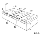
- a corresponding equivalent is shown in FIG. 5.
- This structure then has two barrier layers 3a, 3b, which are produced by Schottky contacts 4a, 4b on the conductive layer (2). Between these two Schottky contacts is an ohmic connection electrode (10), which can be regarded as equivalent to the base connection of a lateral transistor and is provided with the connection (11).
- the two potential peaks which are generated by the barrier layers 3a and 3b are arranged symmetrically with respect to this connection electrode (10).
- connection electrodes (7) or (9) Their distance from the outer connection electrodes (7) or (9) is greater than that from the middle connection electrode (10), so that triangular barriers arise.
- the distance between the potential maximum of the two potential values is preferably less than 0.2 ⁇ m. This small distance between the two potential peaks must be chosen to ensure that electrons that cross the barrier below the Schottky electrode 4a in are able, as hot electrons, to traverse the spatial area in the area of the connection electrode (10) without significant interference, in order then to be able to overcome the potential mountain located below the Schottky electrode 4b if the electrode (9) is appropriately pretensioned.
Landscapes
- Electrodes Of Semiconductors (AREA)
- Bipolar Transistors (AREA)
- Junction Field-Effect Transistors (AREA)
- Semiconductor Integrated Circuits (AREA)
Applications Claiming Priority (2)
| Application Number | Priority Date | Filing Date | Title |
|---|---|---|---|
| DE19863639433 DE3639433A1 (de) | 1986-11-18 | 1986-11-18 | Halbleiteranordnung |
| DE3639433 | 1986-11-18 |
Publications (2)
| Publication Number | Publication Date |
|---|---|
| EP0268136A2 true EP0268136A2 (fr) | 1988-05-25 |
| EP0268136A3 EP0268136A3 (fr) | 1989-03-15 |
Family
ID=6314232
Family Applications (1)
| Application Number | Title | Priority Date | Filing Date |
|---|---|---|---|
| EP87116138A Withdrawn EP0268136A3 (fr) | 1986-11-18 | 1987-11-03 | Dispositif semi-conducteur |
Country Status (4)
| Country | Link |
|---|---|
| US (1) | US4974037A (fr) |
| EP (1) | EP0268136A3 (fr) |
| JP (1) | JPS63136574A (fr) |
| DE (1) | DE3639433A1 (fr) |
Cited By (1)
| Publication number | Priority date | Publication date | Assignee | Title |
|---|---|---|---|---|
| EP0366861A1 (fr) * | 1988-10-20 | 1990-05-09 | International Business Machines Corporation | Transistor balistique semi-conducteur |
Families Citing this family (3)
| Publication number | Priority date | Publication date | Assignee | Title |
|---|---|---|---|---|
| USH1570H (en) * | 1993-03-31 | 1996-08-06 | The United States Of America As Represented By The Secretary Of The Army | Variable lateral quantum confinement transistor |
| US7334901B2 (en) * | 2005-04-22 | 2008-02-26 | Ostendo Technologies, Inc. | Low profile, large screen display using a rear projection array system |
| WO2011066862A1 (fr) | 2009-12-03 | 2011-06-09 | Epcos Ag | Transistor bipolaire avec émetteur et collecteur latéraux, et procédé de fabrication |
Family Cites Families (9)
| Publication number | Priority date | Publication date | Assignee | Title |
|---|---|---|---|---|
| GB1175601A (en) * | 1966-03-28 | 1969-12-23 | Matsushita Electronics Corp | Insulated-Gate Field-Effect Transistor |
| USRE29971E (en) * | 1971-07-31 | 1979-04-17 | Zaidan Hojin Hondotai Kenkyn Shinkokai | Field effect semiconductor device having an unsaturated triode vacuum tube characteristic |
| JPS52146186A (en) * | 1976-05-28 | 1977-12-05 | Fujitsu Ltd | Semiconductor device |
| FR2465318A1 (fr) * | 1979-09-10 | 1981-03-20 | Thomson Csf | Transistor a effet de champ a frequence de coupure elevee |
| JPH0624208B2 (ja) * | 1982-07-29 | 1994-03-30 | 日本電気株式会社 | 半導体装置 |
| DE3402517A1 (de) * | 1984-01-26 | 1985-08-01 | Licentia Patent-Verwaltungs-Gmbh, 6000 Frankfurt | Verfahren zum herstellen eines sperrschicht-feldeffekttransistors |
| JPS61150372A (ja) * | 1984-12-25 | 1986-07-09 | Sony Corp | 半導体装置 |
| JPS61174776A (ja) * | 1985-01-30 | 1986-08-06 | Sony Corp | ヘテロ接合電界効果トランジスタ |
| US4632713A (en) * | 1985-07-31 | 1986-12-30 | Texas Instruments Incorporated | Process of making Schottky barrier devices formed by diffusion before contacting |
-
1986
- 1986-11-18 DE DE19863639433 patent/DE3639433A1/de not_active Withdrawn
-
1987
- 1987-10-26 JP JP62268389A patent/JPS63136574A/ja active Pending
- 1987-11-03 EP EP87116138A patent/EP0268136A3/fr not_active Withdrawn
- 1987-11-09 US US07/117,847 patent/US4974037A/en not_active Expired - Lifetime
Cited By (2)
| Publication number | Priority date | Publication date | Assignee | Title |
|---|---|---|---|---|
| EP0366861A1 (fr) * | 1988-10-20 | 1990-05-09 | International Business Machines Corporation | Transistor balistique semi-conducteur |
| US5712491A (en) * | 1988-10-20 | 1998-01-27 | Ibm Corporation | Lateral theta device |
Also Published As
| Publication number | Publication date |
|---|---|
| US4974037A (en) | 1990-11-27 |
| EP0268136A3 (fr) | 1989-03-15 |
| JPS63136574A (ja) | 1988-06-08 |
| DE3639433A1 (de) | 1988-05-26 |
Similar Documents
| Publication | Publication Date | Title |
|---|---|---|
| DE69224709T2 (de) | Halbleiteranordnung mit verbesserter Durchbruchspannungs-Charakteristik | |
| DE69332619T2 (de) | Verfahren zur Herstellung von einem Feldeffektbauelement mit einem isolierten Gatter | |
| DE2611338C3 (de) | Feldeffekttransistor mit sehr kurzer Kanallange | |
| DE2214935C2 (de) | Integrierte MOS-Schaltung | |
| DE69408605T2 (de) | SOI-Transistor | |
| DE2706623C2 (fr) | ||
| DE69201436T2 (de) | Quantentopf-Transistor mit resonantem Tunneleffekt. | |
| DE2547828B2 (de) | Verfahren zur Herstellung eines Speicherelements mit einem Doppelgate-Isolierschicht-Feldeffekttransistor | |
| EP0003231A1 (fr) | Transistor à effet de champ de type MIS à canal court et son procédé de fabrication | |
| EP0360036A2 (fr) | Jonction pn plane à tenue en tension élévée | |
| DE69123950T2 (de) | SOI-Feldeffekttransistor und dessen Herstellungsverfahren | |
| DE102020116653A1 (de) | Siliziumcarbid-halbleiterbauelement | |
| EP0394757A2 (fr) | Procédé pour la fabrication de structures semi-conductrices actives utilisant des structures de base avec une couche à porteur de charge bidimensionelle parallèle à sa surface | |
| DE112018007354T5 (de) | Siliciumcarbid-halbleitereinheit und herstellungsverfahren für dieselbe | |
| DE102004002723B4 (de) | Halbleiterbauelement mit einem SOI-Aufbau | |
| EP0077481A2 (fr) | Dispositif semi-conducteur planaire | |
| EP0095658A2 (fr) | Dispositif semi-conducteur planaire et son procédé de fabrication | |
| EP1003218A1 (fr) | Dispositifs semi-conducteurs comprenant une diode Schottky et une diode ayant une région fortement dopée, et méthodes de fabrication correspondantes | |
| DE2500235C2 (de) | Ein-PN-Übergang-Planartransistor | |
| EP0585263B1 (fr) | Detecteur semiconducteur | |
| WO2003012854A1 (fr) | Structure a semi-conducteurs dotee d'une magnetoresistance | |
| EP0268136A2 (fr) | Dispositif semi-conducteur | |
| EP3387677B1 (fr) | Transistor à semi-conducteur ayant des structures à super-réseau | |
| DE3114971A1 (de) | Dmos-halbleiterbauelement | |
| DE112006002377T5 (de) | Halbleitervorrichtung und Verfahren zum Herstellen einer Halbleitervorrichtung |
Legal Events
| Date | Code | Title | Description |
|---|---|---|---|
| PUAI | Public reference made under article 153(3) epc to a published international application that has entered the european phase |
Free format text: ORIGINAL CODE: 0009012 |
|
| AK | Designated contracting states |
Kind code of ref document: A2 Designated state(s): DE FR GB IT |
|
| PUAL | Search report despatched |
Free format text: ORIGINAL CODE: 0009013 |
|
| RHK1 | Main classification (correction) |
Ipc: H01L 29/80 |
|
| AK | Designated contracting states |
Kind code of ref document: A3 Designated state(s): DE FR GB IT |
|
| 17P | Request for examination filed |
Effective date: 19890328 |
|
| STAA | Information on the status of an ep patent application or granted ep patent |
Free format text: STATUS: THE APPLICATION IS DEEMED TO BE WITHDRAWN |
|
| 18D | Application deemed to be withdrawn |
Effective date: 19920602 |
|
| RIN1 | Information on inventor provided before grant (corrected) |
Inventor name: BENEKING, HEINZ, PROF. DR. RER. NAT. |