EP0268345B1 - Source de courants ajustés - Google Patents
Source de courants ajustés Download PDFInfo
- Publication number
- EP0268345B1 EP0268345B1 EP87303187A EP87303187A EP0268345B1 EP 0268345 B1 EP0268345 B1 EP 0268345B1 EP 87303187 A EP87303187 A EP 87303187A EP 87303187 A EP87303187 A EP 87303187A EP 0268345 B1 EP0268345 B1 EP 0268345B1
- Authority
- EP
- European Patent Office
- Prior art keywords
- switches
- current source
- transistors
- output
- current
- Prior art date
- Legal status (The legal status is an assumption and is not a legal conclusion. Google has not performed a legal analysis and makes no representation as to the accuracy of the status listed.)
- Expired - Lifetime
Links
- 239000003990 capacitor Substances 0.000 claims description 3
- 230000000694 effects Effects 0.000 abstract description 7
- 230000003503 early effect Effects 0.000 abstract description 3
- 238000010586 diagram Methods 0.000 description 5
- 238000012358 sourcing Methods 0.000 description 5
- 238000000034 method Methods 0.000 description 2
- 230000004048 modification Effects 0.000 description 1
- 238000012986 modification Methods 0.000 description 1
- 238000009966 trimming Methods 0.000 description 1
Images


Classifications
-
- G—PHYSICS
- G05—CONTROLLING; REGULATING
- G05F—SYSTEMS FOR REGULATING ELECTRIC OR MAGNETIC VARIABLES
- G05F3/00—Non-retroactive systems for regulating electric variables by using an uncontrolled element, or an uncontrolled combination of elements, such element or such combination having self-regulating properties
- G05F3/02—Regulating voltage or current
- G05F3/08—Regulating voltage or current wherein the variable is DC
- G05F3/10—Regulating voltage or current wherein the variable is DC using uncontrolled devices with non-linear characteristics
- G05F3/16—Regulating voltage or current wherein the variable is DC using uncontrolled devices with non-linear characteristics being semiconductor devices
- G05F3/20—Regulating voltage or current wherein the variable is DC using uncontrolled devices with non-linear characteristics being semiconductor devices using diode- transistor combinations
- G05F3/24—Regulating voltage or current wherein the variable is DC using uncontrolled devices with non-linear characteristics being semiconductor devices using diode- transistor combinations wherein the transistors are of the field-effect type only
Definitions
- This invention relates to current sources and is more in particular directed to a matching current source for providing the same quantity of sink current as source current.
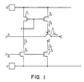
- Fig. 1 illustrates the circuit of a known current source which provides sink current and source current.
- MOS transistors T1 and T2 are serially connected, with the sources of the transistors T1 and T2 being connected to the voltage terminals V+ and V-respectively and the gate of transistors T1 being connected to its drain at node F.
- Node F is also coupled to the gate of transistor T3 having its source connected to the terminal V+.
- Input voltages at node B are applied to the gate of transistor T2 as well as to the gate of a transistor T4 that has its source connected to the voltage terminal V-.
- a voltage node A controls a switch S, for selectively connecting output node C to the drains of the transistors T3 and T4, at terminals D and E respectively.
- Node B controls the amplitude of source current.
- Node C is an output node which is at a fixed voltage in the range between V+ and V-.
- node A controls the switch S to close the contact between C and D and open the contact between C and E, this circuit functions to source current.
- Changes in the voltage applied to node B change the current I1.
- the drain-source voltage Vds1 of transistor T1 and drain-source voltage Vds2 of transistor T2 vary in opposite directions with changes in the voltage of node B. However, the voltage of node C is constant.
- Vds1-Vds2, Vds1-Vds3 and Vds2-Vds4 vary with changes in the voltage of node B.
- Vds1 Vds2, Vds3 and Vds4 are the drain-source voltages of transistors T1, T2, T3 and T4 respectively. Not only transistors T1 and T2, but also transistors T3 and T4, experience the different degree of channel length modulation effect. A linear relationship consequently does not exist between currents I1 and I2, and a linear relationship does not exist between currents I3 and I1. Similarly a linear relation does not exist between currents I2 and I3.
- this circuit can't provide matched current.
- the amplitude of source current in a sourcing current mode is the same as the amplitude of sink current in sinking current mode, independently of whether those currents are large or small.
- a matching current source may be implemented by MOS transistors or bipolar transistors. In spite of the effects of the channel length modulation effect or the Early Effect, the circuit of the invention provides equivalent sink and source current independently of whether the output currents are large or small.
- a matching current source for providing a sink or a source current alternatively, having a first circuit stage comprising first and second transistors; a second circuit stage comprising a third transistor, first and second switches, and a fourth transistor connected in series in that order; control means for selectively setting said first and second switches either to a first state in which the first switch is on and the second switch is off, or to a second state in which the first switch is off and the second switch is on; and an output junction connected between the first and second switches for providing a source current or a sink current depending whether the first and second switches are set to said first or second states; said matching current source being characterized in that it comprises: a set of dummy switches comprising third and fourth constantly on switches connected between said first and second transistors for providing a constant impedance relationship between the first and second circuit stages, and a connecting junction for connecting the third and fourth switches; an operational amplifier comprising an inverting input and having its output coupled to the input electrode of the first transistor and its noninverting
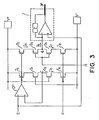
- a matching current source is comprised of two dummy switches (S1, S2), two current switches (S3, S4), four current mirror transistors (T5, T6, T7 and T8) and an operational amplifier OP.
- the transistor T5, switches S1 and S2 and transistor T6 are connected in series in that order between the supply voltage terminals V+ and V-, and the transistor T7, switches S3 and S4 and transistor T8 are connected in series in that order between the terminals V+ and V-.
- the non-inverting input of the amplifier OP is connected to the node I between the switches S1 and S2 and the output of the amplifier is coupled to the gates of the transistors T5 and T7.
- the switches S3 and S4 are controlled by the voltage at node H.
- the voltage at node F is applied to the gates of the transistors T6 and T8.
- the node G at the junction of switches S3 and S4 is connected to the inverting input of an operational amplifier in the feedback circuit 1 and the voltage at node E is applied to the inverting input of the operational amplifier OP as well as to the non-inverting input of the operational amplifier in the feedback circuit 1.
- the feedback circuit may be comprised of the above discussed operational amplifier having a feedback impedance Z, the output terminal J of the feedback circuit having a voltage waveform that is symmetrical in both the sourcing and sinking modes with respect to the voltage V(E) applied to the node E.
- Switches S1 and S2 provide a constant impedance relationship between the first circuit stage (including transistor T5, switch S1, switch S2 and transistor T6 in series) and the second circuit stage (including transistor T7, switch S3, switch S4 and transistor T8 in series).
- the switches S1 and S2 are dummy switches since they are constantly on and their sole purpose is to provide an impedance similar to that of a current switch.
- the voltage applied to node F, coupled to the gates of transistors T6 and T8, controls the amplitudes of the currents I5, I6 and I7.
- the inverting input, node E, of operational amplifier OP is set at a constant voltage.
- the output node G of the matching current source is indirectly set at the same voltage as node E by the feedback circuit 1 of Fig. 2.
- Operational amplifier OP and the first circuit stage comprise a unity gain feedback loop, and therefore nodes E, I and G are held at the same voltage. If the condition: (where L is the channel length of the MOS transistors employed in the circuit, W is channel width of the MOS transistors and X is positive real number) is satisfied, the following conditions will be true:
- FIG. 3 in accordance with a first preferred embodiment of the invention.
- This circuit differs from that of Fig. 2 only in that S1, S2, S3 and S4 are all MOS transistors.
- the gate of the transistor employed for the switch S1 is illustrated as connected to the terminal V- and the gate of the transistor employed for the switch S2 is illustrated as connected to the terminal V+, whereby both of the transistors are always conductive.
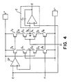
- the feedback circuit 1 of Fig. 3 is replaced by integrator 2 as shown.
- the integrator as illustrated may be comprised of an operational amplifier with a feedback capacitor C1.
- V(H) of Fig. 5(c) is voltage waveform applied to node H of Fig. 4, initially the voltage across the capacitor C1 is zero. If node F is set at a constant voltage, the voltage waveform of the output J of the integrator is the waveform a1 of Fig. 5(a). If node F is set at a different constant voltage, the waveform will change to the waveform a2 of Fig. 5(a).
Landscapes
- Engineering & Computer Science (AREA)
- Microelectronics & Electronic Packaging (AREA)
- Physics & Mathematics (AREA)
- Radar, Positioning & Navigation (AREA)
- Electromagnetism (AREA)
- General Physics & Mathematics (AREA)
- Nonlinear Science (AREA)
- Automation & Control Theory (AREA)
- Amplifiers (AREA)
- Control Of Electrical Variables (AREA)
- External Artificial Organs (AREA)
- Infusion, Injection, And Reservoir Apparatuses (AREA)
- Crystals, And After-Treatments Of Crystals (AREA)
- Led Devices (AREA)
Claims (7)
- Source de courants ajustés possédant un premier étage circuit comprenant des premier et second transistors (T5, T6); un second étage circuit comprenant un troisième transistor (T7), des premier et second commutateurs (S3, S4), et un quatrième transistor (T8) relié en série dans cet ordre; des moyens de commande (H) pour régler de manière sélective lesdits premier et second commutateurs (S3, S4) soit à un premier état dans lequel le premier commutateur (S3) est en circuit et le second commutateur (S4) est hors circuit, ou à un second état dans lequel le premier commutateur (S3) est hors circuit et le second commutateur (S4) est en circuit; et une jonction de sortie (G) reliée entre les premier et second commutateurs (S3, S4) pour fournir un courant de source ou un courant récepteur en fonction du réglage des premier et second commutateurs (S3, S4) aux premier ou second états, ladite source de courants ajustés étant caractérisée en ce qu'elle comprend :
un jeu de commutateurs fictifs comprenant des troisième et quatrième commutateurs constamment en circuit (S1, S2) reliés entre lesdits premier et second transistors (T5, T6) pour fournir une relation d'impédance constante entre les premier et second étages circuits, et une jonction de connexion (I) pour relier les troisième et quatrième commutateurs (S1, S2);
un amplificateur opérationnel (OP) comprenant une entrée inverseuse (E) et dont la sortie est couplée à l'électrode d'entrée du premier transistor (T5) et son entrée non inverseuse couplée à la jonction de connexion (I) entre les troisième et quatrième commutateurs (S1, S2) de façon que l'amplificateur opérationnel (OP) et le premier étage circuit forment un gain unité de la chaîne de retour, la sortie de l'amplificateur opérationnel (OP) étant couplée en outre à l'électrode d'entrée du troisième transistor (TJ); et
un circuit de contreréaction (1) couplé à la jonction de sortie (G) et constituant une borne de sortie (J) de ladite source de courant ajusté, ledit circuit de contreréaction (1) comprenant des moyens pour maintenir la tension à ladite jonction de sortie (G) égale à celle de l'entrée inverseuse (E) de façon que la jonction de connexion (I), l'entrée inverseuse (E) de l'amplificateur opérationnel (OP) et la jonction de sortie (G) soient maintenues à la même tension;
par quoi la source de courants ajustés fournit un courant récepteur ou un courant de source de valeurs équivalentes. - Source de courants ajustés selon la revendication 1, caractérisée en ce que ledit moyen dans le circuit de contreréaction (1) comprend un amplificateur à contreréaction dont la sortie est reliée à la borne de sortie (J), l'entrée inverseuse de celui-ci est couplée à la jonction de sortie (G) et l'entrée non inverseuse de celui-ci couplée à l'entrée inverseuse (E) de l'amplificateur opérationnel (OP).
- Source de courants ajustés selon la revendication 2, caractérisée en ce que le circuit de contreréaction (1) comprend un condensateur relié entre l'entrée inverseuse et la sortie de l'amplificateur à contreréaction de façon que le circuit de contreréaction (1) comprenne un circuit intégré.
- Source de courants ajustés selon l'une des revendications précédentes, caractérisée en ce qu'une relation d'impédance constante est fournie qui répond à la condition :

- Source de courants ajustés selon l'une des revendications précédentes, caractérisée en ce que lesdits les premier et second commutateurs (S3, S4) comprennent des septième et huitième transistors qui sont conducteurs et non conducteurs, respectivement, dans ledit premier état et non conducteurs et conducteurs, respectivement, dans ledit second état.
- Source de courants selon l'une des revendications précédentes, caractérisée en ce que lesdits transistors et commutateurs sont tous des transistors du type MOS.
- Source de courants selon l'une des revendications 1 à 5, caractérisée en ce que lesdits transistors et commutateurs sont tous des transistors bipolaires.
Priority Applications (1)
| Application Number | Priority Date | Filing Date | Title |
|---|---|---|---|
| AT87303187T ATE77498T1 (de) | 1986-11-20 | 1987-04-13 | Angepasste stromquelle. |
Applications Claiming Priority (2)
| Application Number | Priority Date | Filing Date | Title |
|---|---|---|---|
| US932933 | 1986-11-20 | ||
| US06/932,933 US4706013A (en) | 1986-11-20 | 1986-11-20 | Matching current source |
Publications (3)
| Publication Number | Publication Date |
|---|---|
| EP0268345A2 EP0268345A2 (fr) | 1988-05-25 |
| EP0268345A3 EP0268345A3 (en) | 1988-10-12 |
| EP0268345B1 true EP0268345B1 (fr) | 1992-06-17 |
Family
ID=25463172
Family Applications (1)
| Application Number | Title | Priority Date | Filing Date |
|---|---|---|---|
| EP87303187A Expired - Lifetime EP0268345B1 (fr) | 1986-11-20 | 1987-04-13 | Source de courants ajustés |
Country Status (5)
| Country | Link |
|---|---|
| US (1) | US4706013A (fr) |
| EP (1) | EP0268345B1 (fr) |
| JP (1) | JPH0654455B2 (fr) |
| AT (1) | ATE77498T1 (fr) |
| DE (1) | DE3779871T2 (fr) |
Families Citing this family (14)
| Publication number | Priority date | Publication date | Assignee | Title |
|---|---|---|---|---|
| US4904922B1 (en) * | 1985-03-21 | 1992-09-01 | Apparatus for converting between digital and analog values | |
| GB2201535B (en) * | 1987-02-25 | 1990-11-28 | Motorola Inc | Cmos analog multiplying circuit |
| US5266887A (en) * | 1988-05-24 | 1993-11-30 | Dallas Semiconductor Corp. | Bidirectional voltage to current converter |
| US5519309A (en) * | 1988-05-24 | 1996-05-21 | Dallas Semiconductor Corporation | Voltage to current converter with extended dynamic range |
| IT1228034B (it) * | 1988-12-16 | 1991-05-27 | Sgs Thomson Microelectronics | Circuito generatore di corrente a specchi complementari di corrente |
| DE4034371C1 (fr) * | 1990-10-29 | 1991-10-31 | Eurosil Electronic Gmbh, 8057 Eching, De | |
| IT1246598B (it) * | 1991-04-12 | 1994-11-24 | Sgs Thomson Microelectronics | Circuito di riferimento di tensione a band-gap campionato |
| US5153499A (en) * | 1991-09-18 | 1992-10-06 | Allied-Signal Inc. | Precision voltage controlled current source with variable compliance |
| US5453680A (en) * | 1994-01-28 | 1995-09-26 | Texas Instruments Incorporated | Charge pump circuit and method |
| GB9517791D0 (en) * | 1995-08-31 | 1995-11-01 | Philips Electronics Uk Ltd | Current memory |
| DE69739232D1 (de) * | 1997-10-15 | 2009-03-12 | Em Microelectronic Marin Sa | Verfahren zur Herstellung eines sehr genauen Stroms |
| JP3262103B2 (ja) * | 1999-06-07 | 2002-03-04 | 日本電気株式会社 | 内部電源回路を有する半導体装置 |
| US6566851B1 (en) | 2000-08-10 | 2003-05-20 | Applied Micro Circuits, Corporation | Output conductance correction circuit for high compliance short-channel MOS switched current mirror |
| DE10145034B4 (de) | 2001-09-13 | 2005-04-21 | Infineon Technologies Ag | Anordnung mit einer Stromquelle und einem zu dieser in Reihe geschalteten Schalter |
Family Cites Families (7)
| Publication number | Priority date | Publication date | Assignee | Title |
|---|---|---|---|---|
| US3683270A (en) * | 1971-02-22 | 1972-08-08 | Signetics Corp | Integrated circuit bilateral current source |
| NL7700807A (nl) * | 1977-01-27 | 1978-07-31 | Philips Nv | Stroomstabilisator. |
| US4186437A (en) * | 1978-05-03 | 1980-01-29 | California Institute Of Technology | Push-pull switching power amplifier |
| US4283673A (en) * | 1979-12-19 | 1981-08-11 | Signetics Corporation | Means for reducing current-gain modulation due to differences in collector-base voltages on a transistor pair |
| US4532467A (en) * | 1983-03-14 | 1985-07-30 | Vitafin N.V. | CMOS Circuits with parameter adapted voltage regulator |
| ATE37619T1 (de) * | 1984-07-16 | 1988-10-15 | Siemens Ag | Integrierte konstantstromquelle. |
| US4642551A (en) * | 1985-10-22 | 1987-02-10 | Motorola, Inc. | Current to voltage converter circuit |
-
1986
- 1986-11-20 US US06/932,933 patent/US4706013A/en not_active Expired - Lifetime
-
1987
- 1987-04-13 EP EP87303187A patent/EP0268345B1/fr not_active Expired - Lifetime
- 1987-04-13 AT AT87303187T patent/ATE77498T1/de not_active IP Right Cessation
- 1987-04-13 DE DE8787303187T patent/DE3779871T2/de not_active Expired - Fee Related
- 1987-07-13 JP JP62174574A patent/JPH0654455B2/ja not_active Expired - Lifetime
Also Published As
| Publication number | Publication date |
|---|---|
| EP0268345A2 (fr) | 1988-05-25 |
| ATE77498T1 (de) | 1992-07-15 |
| DE3779871D1 (de) | 1992-07-23 |
| JPH0654455B2 (ja) | 1994-07-20 |
| EP0268345A3 (en) | 1988-10-12 |
| DE3779871T2 (de) | 1993-02-04 |
| JPS63138411A (ja) | 1988-06-10 |
| US4706013A (en) | 1987-11-10 |
Similar Documents
| Publication | Publication Date | Title |
|---|---|---|
| US4379267A (en) | Low power differential amplifier | |
| JP2543872B2 (ja) | 増幅回路 | |
| EP0268345B1 (fr) | Source de courants ajustés | |
| US6384684B1 (en) | Amplifier | |
| US4274014A (en) | Switched current source for current limiting complementary symmetry inverter | |
| US20020089351A1 (en) | Integrated circuit and method of controlling output impedance | |
| KR920020847A (ko) | 샘플밴드-갭 전압 기준 회로 | |
| JPH07122946A (ja) | 直列感知抵抗なしの電圧−電流変換器 | |
| US4961046A (en) | Voltage-to-current converter | |
| CA1210090A (fr) | Source de courant cascode | |
| US5218364A (en) | D/a converter with variable biasing resistor | |
| KR950000432B1 (ko) | 트랜지스터 또는 반도체 장치를 시뮬레이팅할 수 있는 회로 및 포락선 검출기 | |
| US5635868A (en) | Power transistor current limiter | |
| US6429685B1 (en) | Integrated circuit and method of controlling output impedance | |
| US4916338A (en) | FET buffer amplifier | |
| EP0156410B1 (fr) | Montage amplificateur | |
| US5903175A (en) | D-type latch circuit and device using the same | |
| KR950005170B1 (ko) | 증폭기 | |
| US4757275A (en) | Wideband closed loop amplifier | |
| EP0157447B1 (fr) | Amplificateur différentiel | |
| US4333025A (en) | N-Channel MOS comparator | |
| JP2896029B2 (ja) | 電圧電流変換回路 | |
| JPH02177724A (ja) | 出力バッファ回路 | |
| US20030020439A1 (en) | Switchable current source | |
| US6507242B1 (en) | Gain switching scheme for amplifiers with digital automatic gain control |
Legal Events
| Date | Code | Title | Description |
|---|---|---|---|
| PUAI | Public reference made under article 153(3) epc to a published international application that has entered the european phase |
Free format text: ORIGINAL CODE: 0009012 |
|
| AK | Designated contracting states |
Kind code of ref document: A2 Designated state(s): AT BE CH DE ES FR GB GR IT LI LU NL SE |
|
| PUAL | Search report despatched |
Free format text: ORIGINAL CODE: 0009013 |
|
| AK | Designated contracting states |
Kind code of ref document: A3 Designated state(s): AT BE CH DE ES FR GB GR IT LI LU NL SE |
|
| 17P | Request for examination filed |
Effective date: 19890118 |
|
| 17Q | First examination report despatched |
Effective date: 19901106 |
|
| GRAA | (expected) grant |
Free format text: ORIGINAL CODE: 0009210 |
|
| AK | Designated contracting states |
Kind code of ref document: B1 Designated state(s): AT BE CH DE ES FR GB GR IT LI LU NL SE |
|
| PG25 | Lapsed in a contracting state [announced via postgrant information from national office to epo] |
Ref country code: SE Effective date: 19920617 Ref country code: GR Free format text: LAPSE BECAUSE OF FAILURE TO SUBMIT A TRANSLATION OF THE DESCRIPTION OR TO PAY THE FEE WITHIN THE PRESCRIBED TIME-LIMIT Effective date: 19920617 Ref country code: AT Effective date: 19920617 |
|
| REF | Corresponds to: |
Ref document number: 77498 Country of ref document: AT Date of ref document: 19920715 Kind code of ref document: T |
|
| REF | Corresponds to: |
Ref document number: 3779871 Country of ref document: DE Date of ref document: 19920723 |
|
| ITF | It: translation for a ep patent filed | ||
| PG25 | Lapsed in a contracting state [announced via postgrant information from national office to epo] |
Ref country code: ES Free format text: LAPSE BECAUSE OF FAILURE TO SUBMIT A TRANSLATION OF THE DESCRIPTION OR TO PAY THE FEE WITHIN THE PRESCRIBED TIME-LIMIT Effective date: 19920928 |
|
| ET | Fr: translation filed | ||
| PLBE | No opposition filed within time limit |
Free format text: ORIGINAL CODE: 0009261 |
|
| STAA | Information on the status of an ep patent application or granted ep patent |
Free format text: STATUS: NO OPPOSITION FILED WITHIN TIME LIMIT |
|
| ITTA | It: last paid annual fee | ||
| PG25 | Lapsed in a contracting state [announced via postgrant information from national office to epo] |
Ref country code: LU Free format text: LAPSE BECAUSE OF NON-PAYMENT OF DUE FEES Effective date: 19930430 |
|
| 26N | No opposition filed | ||
| PGFP | Annual fee paid to national office [announced via postgrant information from national office to epo] |
Ref country code: CH Payment date: 19950313 Year of fee payment: 9 |
|
| PG25 | Lapsed in a contracting state [announced via postgrant information from national office to epo] |
Ref country code: LI Effective date: 19960430 Ref country code: CH Effective date: 19960430 |
|
| REG | Reference to a national code |
Ref country code: CH Ref legal event code: PL |
|
| PGFP | Annual fee paid to national office [announced via postgrant information from national office to epo] |
Ref country code: DE Payment date: 20000410 Year of fee payment: 14 |
|
| PGFP | Annual fee paid to national office [announced via postgrant information from national office to epo] |
Ref country code: FR Payment date: 20000411 Year of fee payment: 14 |
|
| PGFP | Annual fee paid to national office [announced via postgrant information from national office to epo] |
Ref country code: GB Payment date: 20000412 Year of fee payment: 14 |
|
| PGFP | Annual fee paid to national office [announced via postgrant information from national office to epo] |
Ref country code: NL Payment date: 20000428 Year of fee payment: 14 |
|
| PGFP | Annual fee paid to national office [announced via postgrant information from national office to epo] |
Ref country code: BE Payment date: 20000622 Year of fee payment: 14 |
|
| PG25 | Lapsed in a contracting state [announced via postgrant information from national office to epo] |
Ref country code: GB Free format text: LAPSE BECAUSE OF NON-PAYMENT OF DUE FEES Effective date: 20010413 |
|
| PG25 | Lapsed in a contracting state [announced via postgrant information from national office to epo] |
Ref country code: FR Free format text: THE PATENT HAS BEEN ANNULLED BY A DECISION OF A NATIONAL AUTHORITY Effective date: 20010430 Ref country code: BE Free format text: LAPSE BECAUSE OF NON-PAYMENT OF DUE FEES Effective date: 20010430 |
|
| BERE | Be: lapsed |
Owner name: INDUSTRIAL TECHNOLOGY RESEARCH INSTITUTE Effective date: 20010430 |
|
| PG25 | Lapsed in a contracting state [announced via postgrant information from national office to epo] |
Ref country code: NL Free format text: LAPSE BECAUSE OF NON-PAYMENT OF DUE FEES Effective date: 20011101 |
|
| GBPC | Gb: european patent ceased through non-payment of renewal fee |
Effective date: 20010413 |
|
| NLV4 | Nl: lapsed or anulled due to non-payment of the annual fee |
Effective date: 20011101 |
|
| PG25 | Lapsed in a contracting state [announced via postgrant information from national office to epo] |
Ref country code: DE Free format text: LAPSE BECAUSE OF NON-PAYMENT OF DUE FEES Effective date: 20020201 |
|
| REG | Reference to a national code |
Ref country code: FR Ref legal event code: ST |
|
| PG25 | Lapsed in a contracting state [announced via postgrant information from national office to epo] |
Ref country code: IT Free format text: LAPSE BECAUSE OF NON-PAYMENT OF DUE FEES;WARNING: LAPSES OF ITALIAN PATENTS WITH EFFECTIVE DATE BEFORE 2007 MAY HAVE OCCURRED AT ANY TIME BEFORE 2007. THE CORRECT EFFECTIVE DATE MAY BE DIFFERENT FROM THE ONE RECORDED. Effective date: 20050413 |