EP0268513B1 - Einrichtung zur Steuerung eines aus mehreren isolierbaren Segmenten bestehenden Bus - Google Patents
Einrichtung zur Steuerung eines aus mehreren isolierbaren Segmenten bestehenden Bus Download PDFInfo
- Publication number
- EP0268513B1 EP0268513B1 EP19870402370 EP87402370A EP0268513B1 EP 0268513 B1 EP0268513 B1 EP 0268513B1 EP 19870402370 EP19870402370 EP 19870402370 EP 87402370 A EP87402370 A EP 87402370A EP 0268513 B1 EP0268513 B1 EP 0268513B1
- Authority
- EP
- European Patent Office
- Prior art keywords
- segment
- signal
- control
- nac2
- nac1
- Prior art date
- Legal status (The legal status is an assumption and is not a legal conclusion. Google has not performed a legal analysis and makes no representation as to the accuracy of the status listed.)
- Expired - Lifetime
Links
Images
Classifications
-
- G—PHYSICS
- G06—COMPUTING OR CALCULATING; COUNTING
- G06F—ELECTRIC DIGITAL DATA PROCESSING
- G06F13/00—Interconnection of, or transfer of information or other signals between, memories, input/output devices or central processing units
- G06F13/38—Information transfer, e.g. on bus
- G06F13/40—Bus structure
- G06F13/4063—Device-to-bus coupling
- G06F13/4068—Electrical coupling
- G06F13/4072—Drivers or receivers
- G06F13/4077—Precharging or discharging
-
- G—PHYSICS
- G06—COMPUTING OR CALCULATING; COUNTING
- G06F—ELECTRIC DIGITAL DATA PROCESSING
- G06F15/00—Digital computers in general; Data processing equipment in general
- G06F15/76—Architectures of general purpose stored program computers
- G06F15/78—Architectures of general purpose stored program computers comprising a single central processing unit
- G06F15/7896—Modular architectures, e.g. assembled from a number of identical packages
Definitions
- the invention relates to a device for controlling the communication of several electrically isolable bus segments.
- Each segment being generally connected to the output terminals of circuits that can transmit or receive digital information, the communication of two or more segments then allows information to be exchanged between the circuits of one of the segments and the circuits of another. segment (see US-A-4296469 for example).
- Buses which can be subdivided into several segments find an interesting application in particular in the processing units of computers. Indeed, to be able to make several functional sub-assemblies of the unit work simultaneously and independently, it is necessary to be able to isolate the circuits of these sub-assemblies. On the other hand, we must also be able to put two functional subsets into communication with each other. As an example of subsets, we can cite operators, registers or banks of registers. To solve the previous problem, a solution consists in providing means making it possible to isolate segments of the bus at will, each segment being connected to the circuits constituting a functional sub-assembly.
- switches are used, a switch connecting two homologous lines of two adjacent segments. These switches are controlled by selection signals from the computer control unit. The logic state of the selection signals thus defines a certain configuration of the bus. Several segments can be put in series while others will be completely isolated.
- buses which can be subdivided into numerous independent segments. It must also be possible to connect two or more arbitrary segments, which can lead to a situation where the total capacity of the bus is very high. Means should then be used to maintain the voltages of the transmitted signals at a sufficient level over the entire length of the bus.
- each segment of the bus is associated with amplification means which are activated each time the segment works in transmission, in transmission or in reception.
- the invention proposes a device for controlling such a bus according to which the activation of the amplifier of any segment is subject to the activation of the amplifier of that of the adjacent segments which has already been activated.
- the subject of the invention is a bus control device constituted by several isolable segments, allowing the transfer of information from one segment to another, two adjacent segments being interconnected by switches controlled by a selection signal.
- an amplification device controlled by a activation signal being associated with each segment of the bus to amplify the voltages appearing on the lines of said segment, said control device being characterized in that it comprises servo means for activating the amplifier of any segment by response to the activation of the amplifier of a segment adjacent to said segment and to the selection signal of the switches connecting said segment to said adjacent segment.
- the functional sub-assemblies connected to a bus segment can be elements used in read-only mode such as for example operators or else elements which can work in reading or writing, such as for example registers.
- a bus made up of several segments must be able to convey information bidirectionally.
- the switch and amplifier control device should therefore allow this bidirectional operation.
- control device is designed so that it can be triggered during the selection for reading of any segment of the bus.
- the invention also proposes an embodiment of the control device which makes it possible to satisfy these constraints.
- each module being associated with a segment of the bus. More precisely, each module comprises a preloaded control line, the discharge of which activates the amplifier of the associated bus segment, the discharge of this line being able to be controlled by the discharge of a control line associated with one of the adjacent segments.
- this solution has the advantage that one can easily connect to the control line additional discharge means controlled by other signals and thus perform a logical OR function.
- this additional discharge means can be activated in response to a read command signal from one of the circuits connected to the segment associated with the line, thus making it possible to trigger the operation of the command.
- the invention proposes a very simple embodiment using CMOS technology.
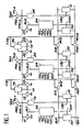
- FIG. 1 shows three segments of a bus of which only two bit lines have been represented for reasons of clarity.
- Bit lines B01, B11 belong to the first segment
- bit lines B02, B12 belong to the second segment
- bit lines B03, B13 belong to the third segment.
- the part of the bus which has been represented corresponds to a single bit of digital information which may include other bits associated with other bit lines not shown.
- Each pair of bit lines such as B01, B11 is connected to the output lines of one or more binary circuits such as M1, which may for example be a memory point or the output circuit associated with a single bit of an operator.
- the binary circuits M2 and M3 are connected respectively to a pair of bit lines of the second and of the third bus segment.
- each binary circuit such as M1, M2, M3 is put into communication with the corresponding bit lines by the action of a selection signal SM1, SM2, SM3 coming from a selection and activation circuit 14, 24, 34 in response to preset and control signals SEL1-SEL3, RD1-RD3, WR1-WR3, PH2, PH3.
- Each pair of bit lines is connected to an amplification device A1, A2, A3 controlled by an activation signal, respectively CA1, CA2, CA3.
- amplification devices can be conventional sense amplifiers commonly used in the memory technique for example.
- Each bit line of a segment is connected to the homologous bit line belonging to an adjacent segment by means of a switch S01, S11, S02, S12.
- a switch S01, S11, S02, S12. For a bus carrying information of several bits, we will thus place as many switches as the bus has lines. All the switches located between two adjacent segments are controlled by the same selection signal C12, C23 which, for a determined logic value, puts these switches in the closed state.
- the three bus segments are respectively associated with the control lines NAC1, NAC2, NAC3.
- Each of the control lines is connected to the input of an amplification circuit 15, 25, 35, the output of which delivers the activation signal CA1, CA2, CA3 from the corresponding amplifier. Thanks to this arrangement, the voltage present on one of the control lines determines the activation of the amplifier of the segment associated with this line. In the perspective of an implementation in CMOS technology, it is in fact the discharge of the line which causes the activation of the corresponding amplifier. Thus to trigger the amplification, it will suffice to provide means for discharging the line that was initially preloaded at a positive voltage.
- the line NAC2 associated with the second segment is connected to ground via a switch 13.
- This switch is controlled by the output signal T1 from a transfer device 16 receiving as input the selection signal C12 of the switches placed between the first two segments.
- the transfer device is also connected at the input to the two control lines NAC1 and NAC2 associated with the first two segments.
- the transfer device 16 is designed so that the signal T1 which it delivers makes the switch 13 conductive when any of the lines NAC1, NAC2 is discharged, provided that the selection signal C12 has the logic value which corresponds when the switches it controls are put into the on state.
- control line NAC1 of the first segment is also connected to a switch 12 also controlled by the output signal T1 from the transfer device 16.
- control line NAC3 associated with the third segment is connected to a switch 23 controlled by another transfer device 26 receiving the switch selection signal placed between the second and the third segment.
- the output signal T2 of the transfer device 26 is applied to the control input of the switch 23.
- the second control line is connected to another switch 22 controlled by the signal T2.
- control lines NAC1, NAC2, NAC3 are also connected to a supply voltage source Vdd by means of switch PC1, PC2, PC3. Each of these switches is controlled by a clock signal PH0.
- control lines NAC1, NAC2, NAC3 are connected to ground by means of additional switches respectively 11, 21, 31 respectively controlled by the signals AC1, AC2, AC3 respectively from circuits 14, 24, 34
- These selection and activation circuits 14, 24, 34 are designed so that they deliver a signal controlling the closing of the corresponding switch 11, 21, 31 when a read control signal RD1, RD2, RD3. is present at their entrance. This arrangement makes it possible to trigger the operation of the control device as soon as a segment is selected for reading.
- FIG. 1 represents only three bus segments, it is obvious that the embodiment described can be generalized for any number of segments.
- the bus control means have a modular structure deduced from the structure of the bus itself.
- the control module can thus constitute a standard cell integrated into a CAD (Computer Aided Design) system.
- CAD Computer Aided Design
- the device operates in at least two phases, one of which corresponds to a precharge phase defined by a clock signal PH0. The purpose of this phase is to charge the control lines at a positive voltage Vdd.
- the read control signals RD1 and selection SEL1 of the first segment are applied to the selection and activation circuit 14. Likewise the selection signals C12 and C23 of the switches are active.
- the circuit 14 delivers on the one hand the selection signal SM1 from one of the circuits of the first segment and on the other hand the control signal AC1 of the discharge switch 11 of the control line NAC1 associated with this segment.
- the circuit M1 is put into communication with the bit lines B01, B11.
- control line NAC1 is discharged by means of the switch 11.
- This discharge activates the amplification circuit 15 which outputs an activation signal CA1 from the amplification device A1.
- the discharge of the control line is detected by the transfer device 16 validated by the selection signal C12.
- the transfer device then causes the activation of the switch 13 of the adjacent line NAC2 causing the discharge of this line.
- this discharge causes the activation of amplifier A2 of the second bus segment.
- the transfer device 26 validated by the signal C23 causes the activation of the switch 23 of the following command line NAC3 which causes the activation of the amplifier A3 of the third segment.
- the write command signal WR3 is applied to the activation and selection circuit 34 as well as the signal preselection SEL3 of circuit M3.
- the circuit 34 delivers the selection signal SM3 to the selected circuit M3.
- This circuit M3 is then placed in communication with the lines B03, B13 whose voltages are at levels allowing writing, thanks to the action of the three amplifiers A1, A2, A3.
- the operation described above in a particular case is easily generalized.
- the number of intermediate segments placed between the first and the last segment can be increased. It is also possible to write-order several segments simultaneously.
- the device can operate bidirectionally. It can also control the transfer of information on either side of the segment ordered for reading.
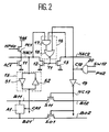
- FIG. 2 represents a more detailed embodiment of the circuits mentioned with reference to FIG. 1.
- This figure shows the two bit lines B01, B11 of the first segment to which the amplification device A1 is connected.
- This segment is connected to an adjacent segment by means of NMOS transistors, S01, S11.
- the drain-source path of each of these transistors is connected in series with the two homologous lines of the two adjacent segments.
- the transistor S01 connects the line B01 of the first segment to the line B02 of the second segment.
- transistor S11 connects line B11 to line B12. This arrangement is reproduced as many times as the information words contain bits.
- the control line NAC1 is connected to the drain of a PMOS-type transistor PC1 (the p-channel MOS transistors are symbolized by a small circle placed on their gate), the source of which is connected to the supply voltage Vdd.
- the gate of this transistor receives the complementary signal NPH0 from the clock signal PH0.
- This transistor PC1 constitutes the means for precharging the control line.
- the control line NAC1 is also connected to the drain of a transistor 12 of the NMOS type, the source of which is connected to ground.
- the adjacent control line NAC2 is connected to the drain of another transistor 13 of NMOS type having its source connected to ground.
- the two transistors 12 and 13 constitute the means for discharging the lines NAC1 and NAC2 respectively.
- the gates of these transistors receive the output signal T1 from the transfer device 16.
- This device consists of an AND gate 17, the two inputs of which are connected respectively to the two control lines NAC1, NAC2.
- the output of this AND gate is connected to an input of a NOR gate 18 whose output provides the signal T1.
- the second input of gate 18 receives the signal C12 from the NAND gate 20.
- This gate receives as input the clock signal PH2 defining the reading phase and the signal SW12 controlling the placing in series of the first and of the second segment.
- the signal C12 is also applied to the input of a power inverter 19, the output of which is connected to the gates of the transistors such as S01, S11 connecting the two adjacent segments.
- the control line NAC1 is connected to the input of an amplification circuit 15 comprising a power inverter 51 whose output provides the activation signal CA1 of the amplifier A1.
- the output of this inverter is also connected to the input of a second inverter 52 whose output is connected to the input of the first inverter 51.
- These two inverters constitute a flip-flop having the dual function of amplifying the signal NAC1 and of maintaining the voltage present on the NAC1 control line.
- the control line NAC1 is also connected to the drain of a transistor 11 of the NMOS type, the source of which is connected to ground.
- the gate of this transistor receives the signal AC1 from circuit 14.
- This latter transistor 11 constitutes the second discharge means described in FIG. 1.
- the signal SW12 takes the logic value 1, which corresponds to a preselection of the closing of the switches connecting the two adjacent segments.
- the clock signal PH0 takes the logic value 1 and the complementary signal NPH0 takes the value 0. It follows that the p-type transistor PC1 is made conductive during this phase. Line NAC1 then charges at a positive voltage Vdd. Note that all the bus command lines will be loaded in the same way.
- the clock signal PH2 takes the logic value 1 and the output signal of the gate 20 takes the logic value 0 while the output voltage NC12 of the power inverter 19 becomes positive making it passable transistors S01, S11.
- the signal AC1 will take the logical value 1 during this phase.
- the transistor 11 will then be conductive, thus discharging the line NAC1.
- the discharge of this line will have two consequences: on the one hand the output of the power inverter 51 will take the logic value 1 thus activating the amplifier A1 of the segment; on the other hand the output of the AND gate 17 will take the logic 0 value and the output T1 of the NOR gate 18 will take a positive voltage thus making the discharge transistor 13 of the line NAC2 conductive.
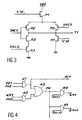
- FIG. 3 represents an embodiment in CMOS technology of the transfer device 16.
- a first transistor P1 of PMOS type the source of which is connected to the supply voltage Vdd receives on its gate the selection signal C12. Its drain is connected to the sources of two other transistors P2, P3 of the PMOS type, the gates of which are connected respectively to the two control lines NAC1 and NAC2. The drains of the two transistors P2, P3 are interconnected, thus constituting the output T1 of the device.
- This point is then connected to the drain of a fourth transistor N1 of NMOS type, the source of which is connected to ground and the gate of which receives the signal C12.
- This same common point is also connected to the drain of a fifth transistor of the NMOS type, the gate of which receives the signal NAC1 and the source of which is connected to the drain of a sixth NOS transistor N3 of which the gate receives the signal NAC2 and the source of which is connected to ground.
- FIG. 4 represents an embodiment of any of the selection and activation circuits 14, 24, 34 shown in FIG. 1.
- This circuit comprises a first AND gate 41 whose two inputs respectively receive the control signal RD1 reading of the bus segment associated with this circuit.
- the other input of the AND gate 41 receives the clock signal PH2 defining the reading phase.
- the output of this AND gate 41 delivers the signal AC1 controlling the discharge of the switch 11.
- a write command signal WR and the clock signal PH3 defining the write phase are applied to the input of a second AND gate 42.
- the outputs of the two AND gates 41, 42 are connected to the input of an OR gate 43.
- FIG. 4 also shows by way of example a fourth AND gate 45 with two inputs receiving respectively the signals PH and SEL11 for preselection of a second circuit of the segment.
- the AND gate 45 delivers the signal SM11 for selecting this circuit. Additional AND gates connected in the same way can be provided if the bus segment is connected to other separately selectable circuits, as is the case for a register bank.
- the circuit of Figure 4 operates as follows. In the case of a read or write command, one of the preset signals SEL1, SEL11 ... takes the logical value 1. If it is a read, the read control signal RD1 has the logical value 1 and the signal AC1 takes this same logical value 1 during the reading phase PH2. Similarly, the signal PH will have the logic value 1 and one of the selection signals SM1, SM11 ... of the preselected circuit will take this same value during the phase PH2. If on the other hand it is a write, the signal WR1 will have the logic value 1, the output of the AND gate 42 taking this same value 1 during the write phase PH3. This will result in setting during this phase PH3 of one of the selection signals SM1, SM11 ... of the circuit preselected for writing. Signal AC1 will keep the logic value 0.
- this circuit allows the activation of the second discharge means 11 of the control line NAC1 associated with the bus segment on which one of these circuits has been selected for reading.
- the associated command line is not discharged under the action of the signal AC1.
- the effective selection of one of the circuits of the segment will take place during the read phase PH2 if the read control signal RD1 is active and during the write phase PH3 if the write control signal WR1 is active.
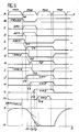
- FIG. 5 represents the timing diagrams of the main signals intervening in the control device according to the invention in the particular case already mentioned where three bus segments would be involved to effect the transfer of information between the first segment selected for reading and the third segment selected in writing.
- the timing diagram A represents the signals defining the four clock phases PH0, PH1, PH2, PH3 used for sequencing the central unit of a computer.
- the PH2 phase is dedicated to read operations
- the PH3 phase to write operations
- the PH0, PH1 phases define the precharge and equalization phases of the bus line voltages.
- Chronogram B represents the selection signals C12 and C23 applied to the switches respectively connecting the first segment to the second segment and the second segment to the third segment.
- the timing diagram C represents the signal SM1 for selecting one of the circuits of the first segment.
- the timing diagram D represents the signal AC1 controlling the discharge switch 11 of the line NAC1.
- the timing diagrams E, G and I respectively represent the voltages present on the three control lines NAC1, NAC2 and NAC3.
- the timing diagrams F and H represent the control signals T1 and T2 respectively from the transfer devices 16 and 26.
- the timing diagrams J, K and L respectively represent the control signals CA1, CA2 and CA3 applied to the three amplifiers A1, A2, A3 of the three segments involved.
- the timing diagram M represents the selection signal SM3 applied to one of the circuits M3 of the third bus segment.
- the timing diagram N represents the variations as a function of time of the voltage present on one of the bit lines of the first segment. This timing diagram corresponds to the case where the bit lines are normally preloaded at a voltage of five volts while the binary value read imposes that the voltage of this line corresponds to a zero voltage.
- the reading phase PH2 begins at time t0 and at this time the bit lines and the control lines are preloaded at the supply voltage.
- the selection signals C12 and C23 are kept at the logic value 0 while the signals SM1 and AC1 keep the logic value 1.
- Setting the signal AC1 to 1 discharges the control line NAC1 which, after a slight delay due to the time constant of this line, goes to the logical value 0 at time t1. This brings the signal CA1 to logic 1 at time t ⁇ 1.
- the signal T1 appearing at the output of the transfer device 16 goes to logic value 1 and this signal causes the discharge of the line NAC2 at the instant t2, after a delay due to the time constant of this line.
- the discharge of line NAC2 in turn causes logic 1 to be set at time t CA2 of the signal CA2 for controlling the amplifier of the second segment.
- This discharge also causes the signal T2 present at the output of the second transfer device 26 to be put to logic 1.
- the signal T2 then causes the command line NAC3 to be discharged, which then takes the logic value 0 at time t3.
- This discharge then causes the signal CA3 to be set to 1, which then activates the amplifier of this third segment.
- the voltage represented on the timing diagram N reflects the successive activations of the three amplifiers A1, A2, A3 respectively at times t ⁇ 1, t ⁇ 2, t ⁇ 3.
- the selection signal SM3 of one of the circuits of the third segment takes the value 1 logic allowing writing in this circuit, during this phase.
- phase PH0 the precharge switches PC1, PC2, PC3 are closed, which causes all the bus control lines to be set to 1.
- the signals T1 and T2 are reset to zero as well as the control signals of the amplifiers CA1, CA2, CA3.
- the corresponding amplifiers A1, A2, A3 are then deactivated, which then allows the preloading of the bus lines.
- control device shows that the activation of the amplifiers is carried out successively by a propagation of the control signals accompanying the propagation of the information transmitted by the different bus segments.
- the capacity of the control lines must be sufficient to introduce time constants introducing an appropriate delay between the activation of two successive amplifiers to leave them sufficient amplification time.
- the capacity of the control lines can be easily calculated and obtained by dimensioning the structure capacities of the MOS transistors used.
Landscapes
- Engineering & Computer Science (AREA)
- Theoretical Computer Science (AREA)
- Computer Hardware Design (AREA)
- General Engineering & Computer Science (AREA)
- Physics & Mathematics (AREA)
- General Physics & Mathematics (AREA)
- Logic Circuits (AREA)
- Control By Computers (AREA)
- Dram (AREA)
Claims (10)
Applications Claiming Priority (2)
| Application Number | Priority Date | Filing Date | Title |
|---|---|---|---|
| FR8614717 | 1986-10-23 | ||
| FR8614717A FR2605768B1 (fr) | 1986-10-23 | 1986-10-23 | Dispositif de commande de bus constitue par plusieurs segments isolables |
Publications (2)
| Publication Number | Publication Date |
|---|---|
| EP0268513A1 EP0268513A1 (de) | 1988-05-25 |
| EP0268513B1 true EP0268513B1 (de) | 1991-02-20 |
Family
ID=9340109
Family Applications (1)
| Application Number | Title | Priority Date | Filing Date |
|---|---|---|---|
| EP19870402370 Expired - Lifetime EP0268513B1 (de) | 1986-10-23 | 1987-10-22 | Einrichtung zur Steuerung eines aus mehreren isolierbaren Segmenten bestehenden Bus |
Country Status (5)
| Country | Link |
|---|---|
| US (1) | US4922409A (de) |
| EP (1) | EP0268513B1 (de) |
| JP (1) | JPH0618020B2 (de) |
| DE (1) | DE3768071D1 (de) |
| FR (1) | FR2605768B1 (de) |
Families Citing this family (19)
| Publication number | Priority date | Publication date | Assignee | Title |
|---|---|---|---|---|
| US5396599A (en) * | 1990-01-16 | 1995-03-07 | Nec Electronics, Inc. | Computer system with a bus controller |
| JP3118266B2 (ja) * | 1990-03-06 | 2000-12-18 | ゼロックス コーポレイション | 同期セグメントバスとバス通信方法 |
| WO1993025968A1 (en) * | 1992-06-10 | 1993-12-23 | Furtek Frederick C | A modular computer based on reconfigurable logic |
| US5740386A (en) * | 1995-05-24 | 1998-04-14 | Dell Usa, L.P. | Adaptive expansion bus |
| US5958033A (en) * | 1997-08-13 | 1999-09-28 | Hewlett Packard Company | On- the-fly partitionable computer bus for enhanced operation with varying bus clock frequencies |
| JPH1173258A (ja) * | 1997-08-28 | 1999-03-16 | Toshiba Corp | 低消費電力バス構造及びその制御方法、低消費電力バス構造の合成システム及びその合成方法、携帯情報機器 |
| AUPQ005099A0 (en) * | 1999-04-29 | 1999-05-20 | Canon Kabushiki Kaisha | Sequential bus architecture |
| DE19960243A1 (de) * | 1999-12-14 | 2001-07-05 | Infineon Technologies Ag | Bussystem |
| US6662260B1 (en) | 2000-03-28 | 2003-12-09 | Analog Devices, Inc. | Electronic circuits with dynamic bus partitioning |
| JP2001318879A (ja) * | 2000-05-11 | 2001-11-16 | Fuji Photo Film Co Ltd | 集積回路およびその制御方法 |
| US6636924B1 (en) * | 2000-08-17 | 2003-10-21 | Koninklijke Philips Electronics N.V. | Multiple port I2C hub |
| FI20011257A0 (fi) * | 2001-06-13 | 2001-06-13 | Nokia Corp | Menetelmä väylän mukauttamiseksi ja väylä |
| EP2383660B1 (de) * | 2005-04-21 | 2013-06-26 | Violin Memory, Inc. | Verbindungssystem |
| US8452929B2 (en) * | 2005-04-21 | 2013-05-28 | Violin Memory Inc. | Method and system for storage of data in non-volatile media |
| US9582449B2 (en) | 2005-04-21 | 2017-02-28 | Violin Memory, Inc. | Interconnection system |
| US8112655B2 (en) * | 2005-04-21 | 2012-02-07 | Violin Memory, Inc. | Mesosynchronous data bus apparatus and method of data transmission |
| US9384818B2 (en) * | 2005-04-21 | 2016-07-05 | Violin Memory | Memory power management |
| US9286198B2 (en) | 2005-04-21 | 2016-03-15 | Violin Memory | Method and system for storage of data in non-volatile media |
| US8028186B2 (en) * | 2006-10-23 | 2011-09-27 | Violin Memory, Inc. | Skew management in an interconnection system |
Family Cites Families (9)
| Publication number | Priority date | Publication date | Assignee | Title |
|---|---|---|---|---|
| US4302642A (en) * | 1977-08-24 | 1981-11-24 | Westinghouse Electric Corp. | Vacuum switch assembly |
| DE2742035A1 (de) * | 1977-09-19 | 1979-03-29 | Siemens Ag | Rechnersystem |
| US4296469A (en) * | 1978-11-17 | 1981-10-20 | Motorola, Inc. | Execution unit for data processor using segmented bus structure |
| JPS57187726A (en) * | 1981-05-13 | 1982-11-18 | Matsushita Electric Ind Co Ltd | Digital circuit |
| DE3268099D1 (en) * | 1982-06-15 | 1986-02-06 | Ibm | Method and apparatus for controlling access to a communication network |
| JPS5962222A (ja) * | 1982-10-01 | 1984-04-09 | Nippon Telegr & Teleph Corp <Ntt> | デイジタル信号入力回路 |
| US4635192A (en) * | 1983-12-06 | 1987-01-06 | Tri Sigma Corporation | Self configuring bus structure for computer network |
| US4737656A (en) * | 1986-04-02 | 1988-04-12 | Izumi Corporation Industries, Inc. | Multiple switch control system |
| DE3615052A1 (de) * | 1986-05-03 | 1987-11-05 | Balluff Gebhard Feinmech | Zweidraht-schalter |
-
1986
- 1986-10-23 FR FR8614717A patent/FR2605768B1/fr not_active Expired
-
1987
- 1987-10-22 JP JP26553587A patent/JPH0618020B2/ja not_active Expired - Lifetime
- 1987-10-22 EP EP19870402370 patent/EP0268513B1/de not_active Expired - Lifetime
- 1987-10-22 DE DE8787402370T patent/DE3768071D1/de not_active Expired - Lifetime
- 1987-10-22 US US07/111,260 patent/US4922409A/en not_active Expired - Lifetime
Also Published As
| Publication number | Publication date |
|---|---|
| FR2605768B1 (fr) | 1989-05-05 |
| JPS63120321A (ja) | 1988-05-24 |
| DE3768071D1 (de) | 1991-03-28 |
| FR2605768A1 (fr) | 1988-04-29 |
| US4922409A (en) | 1990-05-01 |
| JPH0618020B2 (ja) | 1994-03-09 |
| EP0268513A1 (de) | 1988-05-25 |
Similar Documents
| Publication | Publication Date | Title |
|---|---|---|
| EP0268513B1 (de) | Einrichtung zur Steuerung eines aus mehreren isolierbaren Segmenten bestehenden Bus | |
| EP0674264B1 (de) | Schaltung zum Wählen von Redundanzspeicherbauelementen und diese enthaltende FLASH EEPROM | |
| EP0270410B1 (de) | Integrierte Logikschaltung mit EPROM | |
| EP1434237B1 (de) | Nichtflüchtige SRAM Speicherzelle | |
| WO2013160615A1 (fr) | Dispositif logique reprogrammable resistant aux rayonnements | |
| FR2816751A1 (fr) | Memoire flash effacable par page | |
| FR2480504A1 (fr) | Transistor programmable et effacable electriquement | |
| EP1107259A1 (de) | Leseschaltung für integrierte Speicherschaltung | |
| FR2687488A1 (fr) | Dispositif pour memoire a semi-conducteurs avec un circuit de generation d'un signal d'horloge pour des lignes de bit separees. | |
| FR2680025A1 (fr) | Circuit de transmission de donnees comportant une ligne d'entree/sortie commune. | |
| FR2493641A1 (fr) | Reseau logique integre a programmation electrique simplifiee | |
| FR2475269A1 (fr) | Procede de synchronisation d'elevation de tension dans une memoire dynamique a semi-conducteur | |
| FR2801419A1 (fr) | Procede et dispositif de lecture pour memoire en circuit integre | |
| FR2694121A1 (fr) | Mémoire en circuit intégré avec préchaarge préalable en sortie. | |
| EP0601922B1 (de) | Mehrbitwort organisierter EEPROM Speicher | |
| EP4020479B1 (de) | Differentielles lesen eines rram-speichers mit geringem stromverbrauch | |
| FR2718559A1 (fr) | Mémoire non volatile modifiable électriquement incorporant des fonctions de test. | |
| EP0537083B1 (de) | Vorrichtung zum Lesen eines Speicherzelleinhalts, insbesondere für ein EPROM, Betriebsverfahren und Speicher mit einer solchen Vorrichtung | |
| EP0875899B1 (de) | Anordnung von zwei Speichern auf der selben monolitischen integrierten Schaltung | |
| FR2828758A1 (fr) | Procede d'ecriture dans une memoire ram comportant un systeme d'effacement de colonnes | |
| CA1284359C (fr) | Reseau logique dynamique | |
| EP3503105B1 (de) | Adaptierter partitionierter speicherschaltkreis zur durchführung von rechenoperationen | |
| EP1256961B1 (de) | Nichtflüchtige Speicherarchitektur und integrierte Schaltung mit diesem Speicher | |
| EP0845783B1 (de) | Speicherleseschaltung | |
| FR2634576A1 (fr) | Etage de pilotage de lecture et de programmation pour composant a reseau logique programmable |
Legal Events
| Date | Code | Title | Description |
|---|---|---|---|
| PUAI | Public reference made under article 153(3) epc to a published international application that has entered the european phase |
Free format text: ORIGINAL CODE: 0009012 |
|
| AK | Designated contracting states |
Kind code of ref document: A1 Designated state(s): DE FR GB IT NL SE |
|
| 17P | Request for examination filed |
Effective date: 19880609 |
|
| 17Q | First examination report despatched |
Effective date: 19900517 |
|
| GRAA | (expected) grant |
Free format text: ORIGINAL CODE: 0009210 |
|
| AK | Designated contracting states |
Kind code of ref document: B1 Designated state(s): DE FR GB IT NL SE |
|
| GBT | Gb: translation of ep patent filed (gb section 77(6)(a)/1977) | ||
| REF | Corresponds to: |
Ref document number: 3768071 Country of ref document: DE Date of ref document: 19910328 |
|
| ITF | It: translation for a ep patent filed | ||
| PLBE | No opposition filed within time limit |
Free format text: ORIGINAL CODE: 0009261 |
|
| STAA | Information on the status of an ep patent application or granted ep patent |
Free format text: STATUS: NO OPPOSITION FILED WITHIN TIME LIMIT |
|
| 26N | No opposition filed | ||
| EAL | Se: european patent in force in sweden |
Ref document number: 87402370.8 |
|
| REG | Reference to a national code |
Ref country code: GB Ref legal event code: IF02 |
|
| PGFP | Annual fee paid to national office [announced via postgrant information from national office to epo] |
Ref country code: DE Payment date: 20040924 Year of fee payment: 18 Ref country code: SE Payment date: 20040924 Year of fee payment: 18 |
|
| PGFP | Annual fee paid to national office [announced via postgrant information from national office to epo] |
Ref country code: FR Payment date: 20050831 Year of fee payment: 19 |
|
| PGFP | Annual fee paid to national office [announced via postgrant information from national office to epo] |
Ref country code: GB Payment date: 20050926 Year of fee payment: 19 |
|
| PG25 | Lapsed in a contracting state [announced via postgrant information from national office to epo] |
Ref country code: SE Free format text: LAPSE BECAUSE OF NON-PAYMENT OF DUE FEES Effective date: 20051023 |
|
| PG25 | Lapsed in a contracting state [announced via postgrant information from national office to epo] |
Ref country code: DE Free format text: LAPSE BECAUSE OF NON-PAYMENT OF DUE FEES Effective date: 20060503 |
|
| EUG | Se: european patent has lapsed | ||
| PGFP | Annual fee paid to national office [announced via postgrant information from national office to epo] |
Ref country code: NL Payment date: 20060927 Year of fee payment: 20 |
|
| PGFP | Annual fee paid to national office [announced via postgrant information from national office to epo] |
Ref country code: IT Payment date: 20061031 Year of fee payment: 20 |
|
| GBPC | Gb: european patent ceased through non-payment of renewal fee |
Effective date: 20061022 |
|
| REG | Reference to a national code |
Ref country code: FR Ref legal event code: ST Effective date: 20070629 |
|
| PG25 | Lapsed in a contracting state [announced via postgrant information from national office to epo] |
Ref country code: GB Free format text: LAPSE BECAUSE OF NON-PAYMENT OF DUE FEES Effective date: 20061022 |
|
| NLV7 | Nl: ceased due to reaching the maximum lifetime of a patent |
Effective date: 20071022 |
|
| PG25 | Lapsed in a contracting state [announced via postgrant information from national office to epo] |
Ref country code: NL Free format text: LAPSE BECAUSE OF EXPIRATION OF PROTECTION Effective date: 20071022 |
|
| PG25 | Lapsed in a contracting state [announced via postgrant information from national office to epo] |
Ref country code: FR Free format text: LAPSE BECAUSE OF NON-PAYMENT OF DUE FEES Effective date: 20061031 |