EP0268859A2 - Méthode de division d'une plaque semi-conductrice - Google Patents
Méthode de division d'une plaque semi-conductrice Download PDFInfo
- Publication number
- EP0268859A2 EP0268859A2 EP87115785A EP87115785A EP0268859A2 EP 0268859 A2 EP0268859 A2 EP 0268859A2 EP 87115785 A EP87115785 A EP 87115785A EP 87115785 A EP87115785 A EP 87115785A EP 0268859 A2 EP0268859 A2 EP 0268859A2
- Authority
- EP
- European Patent Office
- Prior art keywords
- pellets
- semiconductor
- semiconductor pellets
- wafer
- sized
- Prior art date
- Legal status (The legal status is an assumption and is not a legal conclusion. Google has not performed a legal analysis and makes no representation as to the accuracy of the status listed.)
- Withdrawn
Links
Images


Classifications
-
- G—PHYSICS
- G03—PHOTOGRAPHY; CINEMATOGRAPHY; ANALOGOUS TECHNIQUES USING WAVES OTHER THAN OPTICAL WAVES; ELECTROGRAPHY; HOLOGRAPHY
- G03F—PHOTOMECHANICAL PRODUCTION OF TEXTURED OR PATTERNED SURFACES, e.g. FOR PRINTING, FOR PROCESSING OF SEMICONDUCTOR DEVICES; MATERIALS THEREFOR; ORIGINALS THEREFOR; APPARATUS SPECIALLY ADAPTED THEREFOR
- G03F7/00—Photomechanical, e.g. photolithographic, production of textured or patterned surfaces, e.g. printing surfaces; Materials therefor, e.g. comprising photoresists; Apparatus specially adapted therefor
- G03F7/70—Microphotolithographic exposure; Apparatus therefor
- G03F7/70425—Imaging strategies, e.g. for increasing throughput or resolution, printing product fields larger than the image field or compensating lithography- or non-lithography errors, e.g. proximity correction, mix-and-match, stitching or double patterning
- G03F7/70433—Layout for increasing efficiency or for compensating imaging errors, e.g. layout of exposure fields for reducing focus errors; Use of mask features for increasing efficiency or for compensating imaging errors
-
- H—ELECTRICITY
- H10—SEMICONDUCTOR DEVICES; ELECTRIC SOLID-STATE DEVICES NOT OTHERWISE PROVIDED FOR
- H10P—GENERIC PROCESSES OR APPARATUS FOR THE MANUFACTURE OR TREATMENT OF DEVICES COVERED BY CLASS H10
- H10P52/00—Grinding, lapping or polishing of wafers, substrates or parts of devices
-
- H—ELECTRICITY
- H10—SEMICONDUCTOR DEVICES; ELECTRIC SOLID-STATE DEVICES NOT OTHERWISE PROVIDED FOR
- H10P—GENERIC PROCESSES OR APPARATUS FOR THE MANUFACTURE OR TREATMENT OF DEVICES COVERED BY CLASS H10
- H10P54/00—Cutting or separating of wafers, substrates or parts of devices
Definitions
- This invention relates to a method for manufacturing a semiconductor device, and more particularly to the arrangement of pellets formed in a semiconductor wafer.
- a semiconductor pellet is formed in a square or rectangular plate form with a thickness of 0.1 to 0.5 mm.
- Various kinds of semiconductor pellets are provided and are changed in size and shape according to the types of semiconductor elements such as IC and LSI formed in the pellets.
- the same type of semiconductor pellets are formed in a matrix form on a semiconductor wafer.
- oxidation step, photo-etching step, impurity diffusion step, heat-treatment step and the like are repeatedly performed.
- Pellets having semiconductor elements formed therein are subjected to function test or probe test, and good pellets are separated from defective pellets by marking the defective pellets based on the result of the test.
- the semiconductor wafer is diced or cut apart along dicing lines indicating the boundaries between the semiconductor pellets by, for example, a blade dicer, thereby making a plurality of diced pellets.
- a plurality of semiconductor pellets can be obtained from a single wafer.
- those of the semiconductor pellets located in the peripheral portion of the semiconductor wafer may not be formed in a full square or may have a part cut-away.
- semiconductor pellets having a proper function may not be obtained from the peripheral portion of the wafer. That is, only the central portion of the wafer can be effectively used and the peripheral portion cannot be effectively used to form normal semiconductor pellets.
- An object of this invention is to provide a method for manufacturing a semiconductor device in which substantially the entire portion of a semiconductor wafer can be effectively used by making effective use of the peripheral portion of the wafer.
- the object of this invention can be attained by a method for manufacturing a semiconductor device comprising a wafer processing step of forming large-sized semiconductor pellets in a matrix form in the central area of a semiconductor wafer and forming small-sized semiconductor pellets outside the central area and in the peripheral portion of the semiconductor wafer, thus forming the semiconductor pellets of different sizes in the semiconductor wafer, and a wafer dividing step of dividing the large-sized semiconductor pellets into individual semiconductor pellets and the small-sized semiconductor pellets into individual semiconductor pellets.
- a silicon wafer with a diameter of, for example, 125 mm used as a substrate is prepared.
- the silicon wafer is set in a diffusion furnace and then subjected to oxidation process by passing steam through the furnace to thereby form a silicon oxide film on the surface.
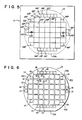
- Fig. 1 shows a glass mask for element formation used in the photo-etching process.
- patterns 12P for forming large-sized semiconductor pellets used as high-power transistors are arranged in a matrix form in the central area of glass mask 11. Patterns 12P are so formed that the outermost pellets will not contact with the outer periphery of the silicon wafer.
- the outer periphery of silicon wafer 13 is indicated by broken lines in Fig. 1.
- Linear portion 13A of silicon wafer 13 indicates the orientation flat portion.
- Target patterns 10A and 10B for mask alignment are formed on a central one of dicing lines between large-sized semiconductor pellet patterns 12P.
- patterns 14P for forming small-sized semiconductor pellets used as low-power transistors are formed in an area between large-sized semiconductor pellet patterns 12P and the outer periphery of silicon wafer 13.
- impurity diffusion process of diffusing impurities of a conductivity type opposite to that of the silicon wafer is effected to form base regions with the patterned silicon oxide film as a mask.
- another photo-etching process is effected to form a mask such as silicon oxide film, photoresist or the like which is used to form emitter regions.
- a glass mask used for forming the mask has pellet patterns for forming large-sized semiconductor pellets in the central area and pellet patterns for forming small-sized semiconductor pellets in the peripheral area.
- conductive material such as aluminum is deposited on the entire surface of the silicon wafer and patterned to form collector, base and emitter electrodes on the collector, base and emitter regions, respectively.
- Fig. 2 shows silicon wafer 13 having semiconductor elements thus formed therein.
- Silicon wafer 13 having semiconductor elements formed therein diced into individual pellets 12 and 14.
- semiconductor pellets 12 and 14 are so arranged that at least one of the dicing lines for semiconductor pellets 12 can also be used as that for semiconductor pellets 14.
- dicing lines 15A, 15B, 15C and 15D are commonly used for dicing large-sized semiconductor pellets 12 and small-sized semiconductor pellets 14. That is, the dicing process is effected by first dicing silicon wafer 13 along dicing lines 15A, 15B, 15C and 15D.
- the pattern structure shown in Fig. 3 is diced along dicing lines extending in horizontal and vertical directions between semiconductor pellets 12 and divided into individual large-sized semiconductor pellets 12.
- Large-sized semiconductor pellets 12 are formed to have an area of, for example, 16.5 x 16.5 mm2, 13.0 x 13.0 mm2 or 11.0 x 11.0 mm2, and an operation current of the power transistor formed in each pellet 12 ranges from 50 A to 100 A.
- the peripheral portion of silicon wafer 13 is diced to divide small-sized semiconductor pellets 14 from one another.
- the peripheral portion obtained by dicing the silicon wafer along dicing line 15A, 15B, 15C or 15D as shown in Fig. 2 cannot be diced with a blade dicer as it is, because the peripheral portion noted above has an area too small to be fixed to the X-Y stage of a blade dicer by vacuum suction. Therefore, it is necessary to thermally attach the diced peripheral portion to dicer cutting tape 16 as shown in Fig. 4. In this case, dicer cutting tape 16 is vacuum-sucked so as to be fixed to the X-Y stage, and then the peripheral portion of silicon wafer 13 can be diced into individual small-sized semiconductor pellets 14.
- Small-sized semiconductor pellets 14 are formed to have an area of, for example, 8.0 x 8.0 mm2. 7.0 x 7.0 mm2 or 6.0 x 6.0 mm2, and an operation current of the power transistor formed in each small-sized semiconductor pellet 14 ranges from 15 to 30 A.
- semiconductor pellets 12 and 14 are divided into groups according to the size and placed on respective chip trays.
- the semiconductor pellets placed on the chip tray are subjected to the function test and determined whether they are good or defective.
- the large-sized semiconductor pellets are arranged in a matrix form in the central area of the silicon wafer and the small-sized semiconductor pellets are arranged in an area between the large-sized semiconductor pellets and the periphery of the silicon wafer which was not used effectively in the prior art, so that the entire portion of the silicon wafer can be effectively used.
- the manufacturing process will not be complicated simply because two different types of semiconductor pellets are formed from a single silicon wafer.
- semiconductor elements in the large-sized semiconductor pellets are formed as large power transistors, and semiconductor elements in the small-sized semiconductor pellets are formed as small power transistors.
- this invention is not limited to this embodiment.
- semiconductor memory devices of large and small capacities can be formed. It is preferable to form large- and small-sized semiconductor pellets which can be manufactured by the same manufacturing method or by using at least some common manufacturing steps.
- a mask is formed to cover the entire surface of the large- or small-sized semiconductor pellets and the different manufacturing step for the small- or large-sized semiconductor pellets is effected so that the different manufacturing steps can be effected without affecting each other.
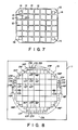
- Figs. 5 to 7 are diagrams for illustrating a method for manufacturing a semiconductor device according to another embodiment of this invention, and respectively correspond to Figs. 1 to 3. Parts in Figs. 5 to 7 which correspond to those in Figs. 1 to 3 are denoted by the same reference numerals, and the detail explanation thereof is omitted.
- additional small-sized semiconductor pellet patterns 14P are formed in areas corresponding to four corners of large-sized semiconductor pellet patterns 12P.
- the additional small-sized semiconductor pellet patterns 14P are formed together with large-sized semiconductor pellet patterns 12P in an area surrounded by dicing lines 15A to 15D.
- the arrangement of semiconductor pellet patterns is advantageous over that in the former embodiment in that the silicon wafer can be more effectively used.
- Figs. 8 and 9 are diagrams for illustrating a method for manufacturing a semiconductor device according to still another embodiment of this invention. Parts in Figs. 8 and 9 which correspond to those in Figs. 1 and 2 are denoted by the same reference numerals.
- semiconductor pellets of two different sizes are obtained from a single silicon wafer.
- semiconductor pellets of three different sizes can be obtained from a single silicon wafer. That is, further small-sized semiconductor pellet patterns 17P which are smaller than small-sized semiconductor pellet patterns 14P are formed in an area between small-sized semiconductor pellet patterns 14P and the periphery of silicon wafer 13.
- the silicon wafer can be further effectively used. Also, in this case, it is necessary to arrange the semiconductor pellets so that the silicon wafer can be diced into areas which each include semiconductor pellets, preferably with the same size, using common dicing lines.
Landscapes
- Physics & Mathematics (AREA)
- General Physics & Mathematics (AREA)
- Dicing (AREA)
Applications Claiming Priority (2)
| Application Number | Priority Date | Filing Date | Title |
|---|---|---|---|
| JP61253865A JPS63108706A (ja) | 1986-10-27 | 1986-10-27 | 半導体装置の製造方法 |
| JP253865/86 | 1986-10-27 |
Publications (2)
| Publication Number | Publication Date |
|---|---|
| EP0268859A2 true EP0268859A2 (fr) | 1988-06-01 |
| EP0268859A3 EP0268859A3 (fr) | 1988-11-09 |
Family
ID=17257204
Family Applications (1)
| Application Number | Title | Priority Date | Filing Date |
|---|---|---|---|
| EP87115785A Withdrawn EP0268859A3 (fr) | 1986-10-27 | 1987-10-27 | Méthode de division d'une plaque semi-conductrice |
Country Status (2)
| Country | Link |
|---|---|
| EP (1) | EP0268859A3 (fr) |
| JP (1) | JPS63108706A (fr) |
Cited By (5)
| Publication number | Priority date | Publication date | Assignee | Title |
|---|---|---|---|---|
| EP0376514A3 (en) * | 1988-12-05 | 1990-11-22 | Xerox Corporation | Fabricating process for lange array semiconductive devices |
| EP0455087A1 (fr) * | 1990-04-24 | 1991-11-06 | Mitsubishi Materials Corporation | Méthode de fabrication d'une plaquette de Silicium munie d'une structure séparatrice de chips, et sections monocristallines |
| EP0709740A1 (fr) * | 1994-09-30 | 1996-05-01 | Texas Instruments Incorporated | Circuit intégré et méthode de fabrication de celui-ci |
| US5531017A (en) * | 1994-02-14 | 1996-07-02 | International Business Machines Corporation | Thin film magnetic head fabrication method |
| EP0768575A3 (fr) * | 1995-10-10 | 1997-11-19 | Deutsche ITT Industries GmbH | Méthode d'optimisation de l'arrangement d'éléments semi-conducteurs sur une plaquette semi-conductrice |
Families Citing this family (1)
| Publication number | Priority date | Publication date | Assignee | Title |
|---|---|---|---|---|
| JP2742710B2 (ja) * | 1989-06-26 | 1998-04-22 | 三菱電機株式会社 | 半導体ウェハ |
Family Cites Families (6)
| Publication number | Priority date | Publication date | Assignee | Title |
|---|---|---|---|---|
| DE2731221A1 (de) * | 1977-07-11 | 1979-02-01 | Semikron Gleichrichterbau | Verfahren zum herstellen von halbleiterkoerpern |
| DE3048362A1 (de) * | 1980-12-20 | 1982-07-29 | Deutsche Itt Industries Gmbh, 7800 Freiburg | "verfahren zur herstellung von halbleiterbauelementen" |
| JPS57143844A (en) * | 1981-02-28 | 1982-09-06 | Matsushita Electric Works Ltd | Chip composition of wafer |
| JPS58137209A (ja) * | 1982-02-09 | 1983-08-15 | Mitsubishi Electric Corp | 半導体装置の製造方法 |
| JPS59220947A (ja) * | 1983-05-30 | 1984-12-12 | Sharp Corp | 半導体装置の製造方法 |
| DE3524301A1 (de) * | 1985-07-06 | 1987-01-15 | Semikron Gleichrichterbau | Verfahren zum herstellen von halbleiterelementen |
-
1986
- 1986-10-27 JP JP61253865A patent/JPS63108706A/ja active Pending
-
1987
- 1987-10-27 EP EP87115785A patent/EP0268859A3/fr not_active Withdrawn
Cited By (6)
| Publication number | Priority date | Publication date | Assignee | Title |
|---|---|---|---|---|
| EP0376514A3 (en) * | 1988-12-05 | 1990-11-22 | Xerox Corporation | Fabricating process for lange array semiconductive devices |
| EP0455087A1 (fr) * | 1990-04-24 | 1991-11-06 | Mitsubishi Materials Corporation | Méthode de fabrication d'une plaquette de Silicium munie d'une structure séparatrice de chips, et sections monocristallines |
| US5804495A (en) * | 1990-04-24 | 1998-09-08 | Mitsubishi Materials Corporation | Method of making SOI structure |
| US5531017A (en) * | 1994-02-14 | 1996-07-02 | International Business Machines Corporation | Thin film magnetic head fabrication method |
| EP0709740A1 (fr) * | 1994-09-30 | 1996-05-01 | Texas Instruments Incorporated | Circuit intégré et méthode de fabrication de celui-ci |
| EP0768575A3 (fr) * | 1995-10-10 | 1997-11-19 | Deutsche ITT Industries GmbH | Méthode d'optimisation de l'arrangement d'éléments semi-conducteurs sur une plaquette semi-conductrice |
Also Published As
| Publication number | Publication date |
|---|---|
| EP0268859A3 (fr) | 1988-11-09 |
| JPS63108706A (ja) | 1988-05-13 |
Similar Documents
| Publication | Publication Date | Title |
|---|---|---|
| US9041162B2 (en) | Wafer and a method of dicing a wafer | |
| US4188707A (en) | Semiconductor devices and method of manufacturing the same | |
| US6624505B2 (en) | Packaged integrated circuits and methods of producing thereof | |
| US5459340A (en) | Adaptive configurable gate array | |
| US6091079A (en) | Semiconductor wafer | |
| EP0343720B1 (fr) | Plaquette semi-conductrice et procédé pour la diviser | |
| US3426252A (en) | Semiconductive device including beam leads | |
| KR100276097B1 (ko) | 필드 프로그램 가능한 상호연결칩 상에 형성되는 앤티퓨즈 장치 및 그 제조방법 | |
| US7601617B2 (en) | Semiconductor wafer and manufacturing method thereof | |
| WO2002051217A2 (fr) | Circuits integres sous boitier et procedes de production de ceux-ci | |
| EP0268859A2 (fr) | Méthode de division d'une plaque semi-conductrice | |
| US3328214A (en) | Process for manufacturing horizontal transistor structure | |
| US3839103A (en) | Semiconductor device and method of manufacturing same | |
| JPH02211648A (ja) | 半導体装置 | |
| US4474639A (en) | Method and device for processing individual integrated circuits into film-mounted, integrated circuits (micropacks) | |
| EP0129915A1 (fr) | Procédé de fabrication d'un dispositif à circuit intégré | |
| US3304594A (en) | Method of making integrated circuit by controlled process | |
| US3513022A (en) | Method of fabricating semiconductor devices | |
| JP3419902B2 (ja) | 電力用半導体装置の製造方法 | |
| US5194931A (en) | Master slice semiconductor device | |
| JP2000164665A (ja) | 半導体集積回路装置及びその製造方法 | |
| EP0402592B1 (fr) | Dispositif semi-conducteur à circuit prédiffusé et son procédé de fabrication | |
| JPH08195387A (ja) | 半導体集積回路装置の製造方法 | |
| JPH11288864A (ja) | アパーチャおよびそれを用いた電子線描画装置の描画方法ならびに半導体装置の製造方法 | |
| JPS6037165A (ja) | 半導体装置の製造方法 |
Legal Events
| Date | Code | Title | Description |
|---|---|---|---|
| PUAI | Public reference made under article 153(3) epc to a published international application that has entered the european phase |
Free format text: ORIGINAL CODE: 0009012 |
|
| 17P | Request for examination filed |
Effective date: 19871027 |
|
| AK | Designated contracting states |
Kind code of ref document: A2 Designated state(s): DE FR GB |
|
| PUAL | Search report despatched |
Free format text: ORIGINAL CODE: 0009013 |
|
| AK | Designated contracting states |
Kind code of ref document: A3 Designated state(s): DE FR GB |
|
| STAA | Information on the status of an ep patent application or granted ep patent |
Free format text: STATUS: THE APPLICATION HAS BEEN WITHDRAWN |
|
| 18W | Application withdrawn |
Withdrawal date: 19881128 |
|
| RIN1 | Information on inventor provided before grant (corrected) |
Inventor name: TANI, KEIZOC/O PATENT DIVISION Inventor name: IWANISHI, MASAAKIC/O PATENT DIVISION Inventor name: TOKIOKA, FUMIOC/O PATENT DIVISION Inventor name: NAKAO, JUNICHIC/O PATENT DIVISION |