EP0269370A2 - Circuit de commande pour accès en mémoire - Google Patents
Circuit de commande pour accès en mémoire Download PDFInfo
- Publication number
- EP0269370A2 EP0269370A2 EP87310226A EP87310226A EP0269370A2 EP 0269370 A2 EP0269370 A2 EP 0269370A2 EP 87310226 A EP87310226 A EP 87310226A EP 87310226 A EP87310226 A EP 87310226A EP 0269370 A2 EP0269370 A2 EP 0269370A2
- Authority
- EP
- European Patent Office
- Prior art keywords
- processing unit
- processing units
- signal
- write
- memory
- Prior art date
- Legal status (The legal status is an assumption and is not a legal conclusion. Google has not performed a legal analysis and makes no representation as to the accuracy of the status listed.)
- Granted
Links
Images





Classifications
-
- G—PHYSICS
- G06—COMPUTING OR CALCULATING; COUNTING
- G06F—ELECTRIC DIGITAL DATA PROCESSING
- G06F3/00—Input arrangements for transferring data to be processed into a form capable of being handled by the computer; Output arrangements for transferring data from processing unit to output unit, e.g. interface arrangements
-
- G—PHYSICS
- G06—COMPUTING OR CALCULATING; COUNTING
- G06F—ELECTRIC DIGITAL DATA PROCESSING
- G06F13/00—Interconnection of, or transfer of information or other signals between, memories, input/output devices or central processing units
- G06F13/14—Handling requests for interconnection or transfer
- G06F13/16—Handling requests for interconnection or transfer for access to memory bus
- G06F13/18—Handling requests for interconnection or transfer for access to memory bus based on priority control
Definitions
- the present invention relates to a memory information transfer unit for transferring associated information from one processing unit to another.
- processing units arranged as described above take much time in internal processing, or require complicated external control apparatus.
- much transfer time is needed from the start to the end of the transfer.
- the present invention seeks to provide a memory access controller for controlling information transfer from a certain processing unit among a plurality of processing units to another with use of the same memory and which is capable of processing for transmission and reception over a short period of time with ease as well as permitting other processing even during transmission and reception.
- a memory access controller associated with a plurality of processing units and equipped with memory means for the common use of said processing units, said memory means being employed when one of said processing units transfers associated information to another of said processing units for writing any information in said memory means and for informing the destination processing unit of the completion of the write operation to thereby permit said destination processing unit to read from said memory means said information so transferred, said controller further comprising:
- a memory access controller where a processing unit writes any information in a memory and informs a destination processing unit of the end of the write operation while the destination processing unit reads the transferred information from the memory, comprising:
- Figure 1 is a circuit block diagram of an embodiment of a memory access controller according to the present invention.
- the apparatus includes a plurality of processing units (not shown, and hereinafter referred to as units), which mutually transfer information, include respectively ports to which symbols P1 and P2 are assigned and possessed by respective signals as designations thereof.
- the buffer memory 30 can write therein and read therefrom information on the basis of write and read requests from the respective ports P1 and P2.
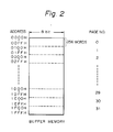
- Figure 2 is an illustration showing the configuration of an embodiment of the buffer memory 30.
- the buffer memory 30, a general purpose type of 8K words X 8 bits, comprises a total of 32 pages from No. 0 to 31. Each page includes 256 words, and each address is given in hexadecimal notation 0000 to lFFF. High order 5 bits and low order 8 bits respectively correspond to the page number and the address number in each page. Those high order 5 bits are employed for specification of the buffer memory upon mutual information transfer between the ports P1 and P2.
- Access timing setting sections 1 and 2 receive a pulse signal from a timing signal generator (not shown) via a pulse signal terminal 20 at predetermined time instincts B, C, E and so on, as shown in the timing charts of Figures 3 to 8.
- the access timing setting section 31 or 32 when kept at a high level (hereinafter referred to as "H") at an input D thereof, issues "H" access timing signals TMA1 and TMA2 at an output Q thereof until their reception of the next pulse signal.
- Access request latch sections 1 and 2 are respectively designated at 33 and 34.
- An accesss port selector section designated at 37, identifies a signal level at the output Q of each of the access request latch sections 33 and 34, and changes only one of its outputs A1 and A2 on the basis of a predetermined selection reference described later before the pulse signal at the pulse signal terminal 20 becomes "H".
- Each of the access timing setting section 31 and 32 sample the signal at its input D with the positive edge at the time instant C to provide the output Q, and maintain that state until the positive edge of the pulse signal at the next time instant C.
- the access request latch sections 33 and 34 when the output Q of each of the access timing setting parts 31 and 32 becomes "H", input the positive edge thereof through their reset terminals R and are thereby reset.
- An OR gate 38 changes a P1 in-access display signal on terminal 10 to "H" as the port P1 being in access while the access request latch section 1, designated at 33 or the access timing setting section 1, designated at 31 stays at “H” at their outputs Q, and indicates to the unit P1 that the port P1 is in communication with the buffer memory.
- an OR gate 39 changes a P2 in-access display signal on terminal 15 to "H" as the port P2 being in access while the access request latch section 2, designated at 34 or the access timing setting section 2, designated at 32, stays at "H” at their outputs Q, and indicates to the P2 unit that the port P2 is in communication with the buffer memory.
- a tri-state buffer 10 (although a plurality of tri-state buffers of the same type are employed, a single tri-state buffer is here depicted instead thereof for brevity.) outputs P1 address signal 13 as address signal AD M of the buffer memory 30 when the access timing setting section 1, designated at 31, has its output Q at "H".
- a tri-state buffer 41 (although a plurality of tri-state buffers are actually employed as in the case of the tri-state buffer 40, a single tri-state buffer is here depicted instead thereof for brevity.) outputs a P2 address signal 18 as the address signal AD M of the buffer memory 30 when the access timing setting section 2, designated at 32, has its output Q at "H".
- An AND gate 42 becomes “H” when the P1 write signal terminal 11 is at "H” and the access timing setting section 1, designated at 31, has its output Q maintained at "H”.
- the AND gate 42 When the output of the AND gate 42 is at "H", information at the P1 data bus signal terminal 14 is passed to the buffer memory 30 as a data bus signal DATA M via the tri-state buffer 43. Simultaneously, the AND gate 42 provides a write signal W M to the buffer memory 30 via an OR gate 44, and writes the content of the data bus signal DATA M in the buffer memory 30 at that time at a specified address AD M thereof.
- An AND gate 45 likewise becomes “H” when a P2 write signal terminal 16 is at “H” and the access timing setting section 2, designated at 32, has its output Q maintained at "H".
- the AND gate 47 once becoming "H", provides an output enable signal R M to the buffer memory 30 via an OR gate 48. Thereupon, the operation provides in the same manner as in the write operation described previously, the information at the P1 address signal terminal 13 as the address signal AD M of the buffer memory 30 via the tri-state buffer 40 in order to enable the word content in the buffer memory 30 at the address AD M to be read.
- the AND gate 49 once becoming “H”, provides an output enable signal R M to the buffer memory 30 via an OR gate 48. Thereupon, this enables information at the P2 address signal terminal 18 to be provided as the address signal AD M of the buffer memory 30 via the tri-state buffer 41 whereby the word content in the buffer memory 30 at the address AD M thereof may be read.
- Data latch sections 1 and 2 designated at 50 and 51 and employed upon each read operation, receive the data bus signal read from the buffer memory 30 at their respective input terminals D IN .
- the respective data latch sections 1 and 2, designated at 50 and 51, receive latch timing by driving the inverters 52 and 53 with the negative edges of the outputs from the AND gates 47 and 49 to latch the content of the data bus signal, and output that data bus signal DATA M from the output terminal D OUT .
- Buffers 54 and 55 feed data at the output terminals D OUT of the respective data latch sections 50 and 51 to the terminals 14 and 19 respectively as the P1 data bus signal and the P2 data bus signal when the P1 and P2 read signal terminals 12 and 17 are respectively at "H".
- Figure 3 is a timing chart of the write operation corresponding to the transfer of information from the port P1 unit to the buffer memory 30.
- the access request latch section 1 designated at 33, changes its output Q to "H” to cause the P1 in-access display signal terminal 10 (DISP1) to become “H", whereby the memory access controller displays that the P1 unit is in access.
- the access port selection section 37 changes its output A1 to "H” owing to the access request latch section 1, designated at 33, becoming "H” at its output Q.
- the access timing setting section 1, designated at 31, has its input terminal D becoming “H”, and receives a pulse signal at its pulse signal terminal 20 at the time instant of B to cause TMA1, the access timing signal at its output Q, to become “H”.
- the write signal W M of the buffer memory 30 becomes "H” as receiving the access timing signal.
- information (AD1) at the P1 address signal terminal 12 involving the page number as the address signal of the buffer memory is provided as the address signal AD M of the buffer memory 30.
- the information (DATA1) at the P1 data bus signal terminal 14 as transfer data is provided as the data bus signal DATA M of the buffer memory 30.
- the access timing signal TMA1 changes to "L" to result in the end of the information write operation.
- the port P1 unit confirms the end of the write operation based upon the DISP1 signal becoming "L” at the time instant C, and thereby changes the P1 write signal W1 to "L” at the time instant D.
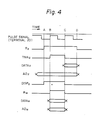
- Figure 4 is a timing chart showing the procedure when the port P2 unit reads the associated information stored in the buffer memory 30.
- the terminal 17 0f Figure 1 (R2 of Figure 4) becomes “H”.
- the access request latch section 2, designated at 34 becomes "H” at its output with the P2 in-access display signal terminal 15 (DISP2) becoming “H", whereby the memory access controller indicates the P2 unit to be in access.
- the access port selection section 37 changes to "H" at its output A2 in response to the access request latch section 2, designated at 34, becoming "H” at its output Q.
- the output timing setting part 2, designated at 32, permits the access timing signal TMA2 at its output Q to become "H" at the time instant B of Figure 4.
- the buffer memory 30 permits the output enable signal R M thereat to become "H”.
- the information (AD2) at the P2 address signal terminal 18 for addressing the buffer memory 30 is provided as the address signal AD M of the buffer memory 30.
- the data latch section 2, designated at 51, receives the information (DATA M ) read from an address specified by the P2 address signal AD2.
- the access timing signal TMA2 becomes "L” at the time instant C, and hence the information read operation from the buffer memory 30 is completed and the P2 in-access display signal DISP2 becomes “L”.
- the data latch section 2 designated at 51, latches the aforementioned read data bus signal DATA M and transfers the same as the P2 data bus signal DATA2 from the terminal 19 to the P2 unit.
- the fact of the DISP2 signal becoming "L” indicates that the P2 data bus signal DATA2 has thereon effectively transmitted the read data.
- the port P2 unit upon reading that transmitted read data, changes the P2 read signal to "L" at the time instant D to complete the read operation from the memory.
- FIG. 5 is a timing chart for a write operation in which a processing unit, which issues an access instruction earlier than the other processing units, is assumed to get priority. Description of each signal on the side of the buffer memory 30 will be omitted here. A situation is illustrated here in which the P1 write signal W1 becomes “H” as the time instant A of the same figure, and successiveively the P2 write signal W2 becomes “H” at the time instant A ⁇ , and then the access timing setting sections 31 and 32 receive a pulse signal at their input terminals C from the pulse signal terminal 20.
- the access request latch sections 33 and 34 respectively become “H” at their outputs Q at the time instants A and A ⁇ to result in both of the signal DISP1 at the P1 in-access display signal terminal 10 and the signal DISP2 at the P2 in-access display signal terminal 15 becoming "H".
- the access port selection section 37 changes to "H" at its output A1 before the time instant B in response to the P1 write signal W1 issued previous to the P2 write signal W2.
- the access timing setting section 1, designated at 31 receives the pulse signal from the pulse signal terminal 20 at the time instant B and issues the access timing signal TMA1.
- the access request latch section 1, designated at 33 changes to "L” at its output Q.
- the access port selection section 37 changes to "L” at its output A1 and to "H” at its output A2 before the time instant C.
- the access timing setting section 2, designated at 32 receives the pulse signal from the pulse signal terminal 20 at the time instant C to change the TMA2 to "H".
- the P1 data bus signal DATA1 is written at an address specified by the AD1 in the period of the access timing TMA1 kept at "H", in the same manner as in the timing chart of Figure 3.
- the P2 data bus signal DATA2 is written in the buffer memory 30 at an address specified by the AD2 during the period in which the access timing TMA2 is kept at "H”.
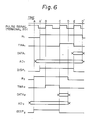
- Figure 6 is a timing chart for the read operation in a situation where a processing unit, which issues an access instruction earlier than the other processing units, takes precedence.
- the P2 read signal R2 precedes the P1 read signal R1.
- the buffer memory 30 permits data at an address specified by the P2 address signal AD2 to be read thereform during the period in which the access timing signal TMA2 is kept at "H", and the data latch section 2, designated at 51, latches the data involved in the data bus signal DATA M at the time instant C.
- the buffer memory 30 permits data at an address specified by the P1 address signal AD1 to be read therefrom during the period in which the access timing sigl TMA1 is kept at "H", and the data latch section 1, designated at 50, latches the data involved in the data bus signal DATA M at the time instant E.
- Figure 7 is a timing chart of the write operation when the port P1 takes precedence over the port P2.
- the P1 write signal W2 is issued earlier than the P1 write signal.
- the access port selection section 37 detects the P1 write signal W1 having priority before the time instant B1 and giving priority thereto to change its output A1 to "H".
- the access timing setting section 1 therefore permits the TMA, the output Q thereof, to become "H" first.
- the access port setting section 37 thereafter changes its output Al to "L” and its output A2 to "H", before the time instant C.
- the TMA1 the signal at the access timing setting section 1, designated at 31, is changed to "L”
- the TMA2 the signal at the access timing setting section 2, designated at 32, is changed to "H”.
- the write operation in the buffer memory 30 proceeds in the same fashion as in the write timing in Figure 3.
- Figure 8 is a timing chart of the read operation in a situation where the port P1 takes precedence over the port P2.
- the P2 read signal R2 is issued before the time instant B, while the P1 read signal R1 is issued after that time instant.
- the port P1 although having priority, does not take precedence, and permits the access timing signal TMA2 on the side of the port P2 to change to "H" at the time instant B, whereby the read operation by the port P2 is executed in the same manner as that of Figure 4.
- the access timing signal TMA1 on the side of the port P1 becomes "H" to permit the port 1 to execute the read operation.
Landscapes
- Engineering & Computer Science (AREA)
- Theoretical Computer Science (AREA)
- Physics & Mathematics (AREA)
- General Engineering & Computer Science (AREA)
- General Physics & Mathematics (AREA)
- Human Computer Interaction (AREA)
- Bus Control (AREA)
- Multi Processors (AREA)
- Memory System (AREA)
- Information Transfer Systems (AREA)
Applications Claiming Priority (2)
| Application Number | Priority Date | Filing Date | Title |
|---|---|---|---|
| JP276859/86 | 1986-11-21 | ||
| JP61276859A JPS63132369A (ja) | 1986-11-21 | 1986-11-21 | メモリ情報転送方式 |
Publications (3)
| Publication Number | Publication Date |
|---|---|
| EP0269370A2 true EP0269370A2 (fr) | 1988-06-01 |
| EP0269370A3 EP0269370A3 (fr) | 1991-05-08 |
| EP0269370B1 EP0269370B1 (fr) | 1996-01-31 |
Family
ID=17575404
Family Applications (1)
| Application Number | Title | Priority Date | Filing Date |
|---|---|---|---|
| EP87310226A Expired - Lifetime EP0269370B1 (fr) | 1986-11-21 | 1987-11-19 | Circuit de commande pour accès en mémoire |
Country Status (6)
| Country | Link |
|---|---|
| EP (1) | EP0269370B1 (fr) |
| JP (1) | JPS63132369A (fr) |
| KR (1) | KR920003174B1 (fr) |
| AU (1) | AU598870B2 (fr) |
| CA (1) | CA1296808C (fr) |
| DE (1) | DE3751693T2 (fr) |
Cited By (1)
| Publication number | Priority date | Publication date | Assignee | Title |
|---|---|---|---|---|
| CN109522249A (zh) * | 2017-09-20 | 2019-03-26 | 东芝存储器株式会社 | 存储器系统 |
Families Citing this family (4)
| Publication number | Priority date | Publication date | Assignee | Title |
|---|---|---|---|---|
| JP2911002B2 (ja) * | 1988-09-20 | 1999-06-23 | ローム 株式会社 | メモリアクセス回路 |
| JPH02140860A (ja) * | 1988-11-22 | 1990-05-30 | Fujitsu Ltd | 中央処理装置間通信命令制御方式 |
| JP2005084907A (ja) | 2003-09-08 | 2005-03-31 | Sony Corp | メモリ帯域制御装置 |
| KR101351846B1 (ko) * | 2012-10-10 | 2014-01-16 | 한국화학연구원 | 올리고에틸렌글라이콜을 곁사슬로 갖는 폴리카보네이트계 가소제를 함유하는 semi―IPN 타입의 고체 고분자 전해질 조성물 |
Family Cites Families (13)
| Publication number | Priority date | Publication date | Assignee | Title |
|---|---|---|---|---|
| US4130864A (en) * | 1976-10-29 | 1978-12-19 | Westinghouse Electric Corp. | Priority selection circuit for multiported central functional unit with automatic priority reduction on excessive port request |
| US4209839A (en) * | 1978-06-16 | 1980-06-24 | International Business Machines Corporation | Shared synchronous memory multiprocessing arrangement |
| US4449183A (en) * | 1979-07-09 | 1984-05-15 | Digital Equipment Corporation | Arbitration scheme for a multiported shared functional device for use in multiprocessing systems |
| IT1126475B (it) * | 1979-12-03 | 1986-05-21 | Honeywell Inf Systems | Apparato di comunicazione tra piu' processori |
| EP0064074B1 (fr) * | 1980-11-10 | 1988-09-14 | Wang Laboratories Inc. | Liaison de transmission de donnees |
| JPS58208862A (ja) * | 1982-05-31 | 1983-12-05 | Toshiba Corp | 共有メモリ制御方式 |
| US4698753A (en) * | 1982-11-09 | 1987-10-06 | Texas Instruments Incorporated | Multiprocessor interface device |
| ZA838188B (en) * | 1982-11-20 | 1984-06-27 | Int Computers Ltd | Data processing system |
| JPS6091473A (ja) * | 1983-10-25 | 1985-05-22 | Oki Electric Ind Co Ltd | メモリマルチアクセス方式 |
| JPS60245063A (ja) * | 1984-05-21 | 1985-12-04 | Fujitsu Ltd | 共用メモリアクセス方式 |
| JPS6128155A (ja) * | 1984-07-19 | 1986-02-07 | Nec Corp | 共有メモリに対する多重アクセス方式 |
| JPS61114362A (ja) * | 1984-11-09 | 1986-06-02 | Oki Electric Ind Co Ltd | 共有メモリアクセス制御方式 |
| JPS61177564A (ja) * | 1985-02-01 | 1986-08-09 | Neoroogu Denshi Kk | 共有記憶装置 |
-
1986
- 1986-11-21 JP JP61276859A patent/JPS63132369A/ja active Pending
-
1987
- 1987-11-19 EP EP87310226A patent/EP0269370B1/fr not_active Expired - Lifetime
- 1987-11-19 DE DE3751693T patent/DE3751693T2/de not_active Expired - Fee Related
- 1987-11-19 KR KR1019870013041A patent/KR920003174B1/ko not_active Expired
- 1987-11-20 AU AU81445/87A patent/AU598870B2/en not_active Ceased
- 1987-11-20 CA CA000552321A patent/CA1296808C/fr not_active Expired - Fee Related
Cited By (2)
| Publication number | Priority date | Publication date | Assignee | Title |
|---|---|---|---|---|
| CN109522249A (zh) * | 2017-09-20 | 2019-03-26 | 东芝存储器株式会社 | 存储器系统 |
| CN109522249B (zh) * | 2017-09-20 | 2022-10-11 | 铠侠股份有限公司 | 存储器系统 |
Also Published As
| Publication number | Publication date |
|---|---|
| DE3751693D1 (de) | 1996-03-14 |
| DE3751693T2 (de) | 1996-09-26 |
| CA1296808C (fr) | 1992-03-03 |
| AU8144587A (en) | 1988-05-26 |
| KR920003174B1 (ko) | 1992-04-23 |
| JPS63132369A (ja) | 1988-06-04 |
| KR880006592A (ko) | 1988-07-23 |
| EP0269370B1 (fr) | 1996-01-31 |
| EP0269370A3 (fr) | 1991-05-08 |
| AU598870B2 (en) | 1990-07-05 |
Similar Documents
| Publication | Publication Date | Title |
|---|---|---|
| US4831514A (en) | Method and device for connecting a 16-bit microprocessor to 8-bit modules | |
| KR970007276B1 (ko) | 데이터 전송장치 | |
| US6384832B1 (en) | Image processing apparatus and image processing system using the apparatus | |
| EP0409285B1 (fr) | Méthode et appareil de transmission de données entre éléments processeurs | |
| JPS61182157A (ja) | 画像処理装置及び相互通信バス装置 | |
| US5481678A (en) | Data processor including selection mechanism for coupling internal and external request signals to interrupt and DMA controllers | |
| US4126897A (en) | Request forwarding system | |
| EP0347929A2 (fr) | Processeurs à traitement parallèle | |
| EP0479702A2 (fr) | Système pour le transfert de données entre des buses utilisant des dispositifs d'accès direct à la mémoire | |
| US4922416A (en) | Interface device end message storing with register and interrupt service registers for directing segmented message transfer between intelligent switch and microcomputer | |
| EP0269370A2 (fr) | Circuit de commande pour accès en mémoire | |
| JP2001084229A (ja) | Simd型プロセッサ | |
| EP0081358B1 (fr) | Système de traitement de données fournissant un transfert de données entre modules | |
| EP0331487B1 (fr) | Système pour commander le transfert de données | |
| US4151375A (en) | System for selectively shifting groups of bits for temporary storage in a processor memory of a telephone exchange | |
| US6591326B1 (en) | Method and information processing apparatus controlling information transfer among a plurality of processors | |
| EP0141753A2 (fr) | Mémoire tampon ajustable pour communication de données dans un système de traitement de données | |
| JPS62182857A (ja) | 入出力制御装置 | |
| US11397581B2 (en) | Data transmission system capable of perform union task with a plurality of channel control modules | |
| US5579483A (en) | Communication controller for controlling multi-channel multiplex communication and having channel selection functions and memory for storing communication control data for each channel | |
| JPH0833869B2 (ja) | データ処理装置 | |
| JPH08123749A (ja) | バスコントローラ | |
| JPH0525133B2 (fr) | ||
| JPS61276050A (ja) | デ−タ転送方式 | |
| JPH06161945A (ja) | メモリデータ転送装置 |
Legal Events
| Date | Code | Title | Description |
|---|---|---|---|
| PUAI | Public reference made under article 153(3) epc to a published international application that has entered the european phase |
Free format text: ORIGINAL CODE: 0009012 |
|
| AK | Designated contracting states |
Kind code of ref document: A2 Designated state(s): DE FR GB IT |
|
| PUAL | Search report despatched |
Free format text: ORIGINAL CODE: 0009013 |
|
| AK | Designated contracting states |
Kind code of ref document: A3 Designated state(s): DE FR GB IT |
|
| RHK1 | Main classification (correction) |
Ipc: G06F 13/18 |
|
| 17P | Request for examination filed |
Effective date: 19910923 |
|
| 17Q | First examination report despatched |
Effective date: 19930601 |
|
| GRAA | (expected) grant |
Free format text: ORIGINAL CODE: 0009210 |
|
| AK | Designated contracting states |
Kind code of ref document: B1 Designated state(s): DE FR GB IT |
|
| ET | Fr: translation filed | ||
| REF | Corresponds to: |
Ref document number: 3751693 Country of ref document: DE Date of ref document: 19960314 |
|
| ITF | It: translation for a ep patent filed | ||
| PLBE | No opposition filed within time limit |
Free format text: ORIGINAL CODE: 0009261 |
|
| STAA | Information on the status of an ep patent application or granted ep patent |
Free format text: STATUS: NO OPPOSITION FILED WITHIN TIME LIMIT |
|
| 26N | No opposition filed | ||
| PGFP | Annual fee paid to national office [announced via postgrant information from national office to epo] |
Ref country code: FR Payment date: 20011113 Year of fee payment: 15 |
|
| PGFP | Annual fee paid to national office [announced via postgrant information from national office to epo] |
Ref country code: GB Payment date: 20011121 Year of fee payment: 15 |
|
| PGFP | Annual fee paid to national office [announced via postgrant information from national office to epo] |
Ref country code: DE Payment date: 20011203 Year of fee payment: 15 |
|
| REG | Reference to a national code |
Ref country code: GB Ref legal event code: IF02 |
|
| PG25 | Lapsed in a contracting state [announced via postgrant information from national office to epo] |
Ref country code: GB Free format text: LAPSE BECAUSE OF NON-PAYMENT OF DUE FEES Effective date: 20021119 |
|
| PG25 | Lapsed in a contracting state [announced via postgrant information from national office to epo] |
Ref country code: DE Free format text: LAPSE BECAUSE OF NON-PAYMENT OF DUE FEES Effective date: 20030603 |
|
| GBPC | Gb: european patent ceased through non-payment of renewal fee | ||
| PG25 | Lapsed in a contracting state [announced via postgrant information from national office to epo] |
Ref country code: FR Free format text: LAPSE BECAUSE OF NON-PAYMENT OF DUE FEES Effective date: 20030731 |
|
| REG | Reference to a national code |
Ref country code: FR Ref legal event code: ST |
|
| PG25 | Lapsed in a contracting state [announced via postgrant information from national office to epo] |
Ref country code: IT Free format text: LAPSE BECAUSE OF NON-PAYMENT OF DUE FEES;WARNING: LAPSES OF ITALIAN PATENTS WITH EFFECTIVE DATE BEFORE 2007 MAY HAVE OCCURRED AT ANY TIME BEFORE 2007. THE CORRECT EFFECTIVE DATE MAY BE DIFFERENT FROM THE ONE RECORDED. Effective date: 20051119 |