EP0270028A2 - Dispositif de mémoire à double accès ayant un schéma d'accès séquentiel - Google Patents
Dispositif de mémoire à double accès ayant un schéma d'accès séquentiel Download PDFInfo
- Publication number
- EP0270028A2 EP0270028A2 EP87117590A EP87117590A EP0270028A2 EP 0270028 A2 EP0270028 A2 EP 0270028A2 EP 87117590 A EP87117590 A EP 87117590A EP 87117590 A EP87117590 A EP 87117590A EP 0270028 A2 EP0270028 A2 EP 0270028A2
- Authority
- EP
- European Patent Office
- Prior art keywords
- columns
- memory
- shift register
- array
- random access
- Prior art date
- Legal status (The legal status is an assumption and is not a legal conclusion. Google has not performed a legal analysis and makes no representation as to the accuracy of the status listed.)
- Withdrawn
Links
Images


Classifications
-
- G—PHYSICS
- G11—INFORMATION STORAGE
- G11C—STATIC STORES
- G11C7/00—Arrangements for writing information into, or reading information out from, a digital store
- G11C7/10—Input/output [I/O] data interface arrangements, e.g. I/O data control circuits, I/O data buffers
- G11C7/1075—Input/output [I/O] data interface arrangements, e.g. I/O data control circuits, I/O data buffers for multiport memories each having random access ports and serial ports, e.g. video RAM
-
- G—PHYSICS
- G11—INFORMATION STORAGE
- G11C—STATIC STORES
- G11C8/00—Arrangements for selecting an address in a digital store
- G11C8/16—Multiple access memory array, e.g. addressing one storage element via at least two independent addressing line groups
Definitions
- the present invention relates to a memory circuit and more particularly to a dual port memory circuit.
- RAMs Random access memories
- MOS random access memories are used for processing video images, especially for displaying images on a CRT.
- a memory device used with such a display is connected between a CPU and the CRT.
- the CPU communicates with the RAM on a random access basis and supplies the display information to the RAM.
- the memory access time depends upon the speed of the CPU. Data transfer from the memory to the CRT is performed on a line-by-line sequential basis rather than on a random access basis. Moreover the speed of such data transfer depends upon the display size of the CRT.
- the speed is determined in dependence upon the required resolution of the CRT.
- VRAM The RAM for data display 'will hereinafter be referred to as a "VRAM".
- VRAM The RAM for data display 'will hereinafter be referred to as a "VRAM".
- RAMs having an inputioutput system for a CPU and an output system for a CRT are the best suitable for use as a VRAM.
- Such RAMs are called a "dual port memory”.
- a known dual port memory is structured such that a shift register is provided to the known RAM and a serial read operation to the CRT is performed via the shift register while performing the usual random access operation by the commonly provided input/output port of the RAM.
- the order of serial read operations through the shift register is fixed. Namely, the serial read operation is always started from the first bit of the shift register. which first bit is located at the bit position closest to the output terminal and advanced towards the final bit of the shift register, which final bit is located at the bit position farthest from the output terminal.
- a counter or a shift register and a decoder for deciding a start bit position in accordance with column address information must be provided in the serial access port to achieve the above feature and therefore, an additional area for the counter and the decoder must be provided on a semiconductor chip on which the memory is formed, is necessitated to enlarge the whole size of the chip. This lowers the yields of the memories. Also, the above memory cause a large power consumption.
- the dual port memory is of the type having a memory cell array arranged in rows and columns, a random access peripheral circuit for performing random access operation with respect to the memory cell array in response to row and column address information, and a serial access peripheral circuit for serially accessing the columns of the array in response to shift clocks.
- the random access port includes a column decoder whose output is used to select a part of columns and the above serial access peripheral circuit includes a shift register whose output is used to select the columns serially and a control circuit for operatively determining the state of the shift register by the output of the column decoder in the random access peripheral circuit.
- the column decoder in the random access peripheral circuit is also used to determine a start position of the shift register.
- the column decoder is shared by both the random access peripheral circuit and the serial access peripheral circuit. Therefore, the area of the memory on a semiconductor chip can be reduced and power consumption caused by the column decoder in the serial access peripheral circuit is avoided.
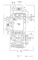
- a RAM unit 100 is identical to the ordinary RAM.
- a row address buffer 101 receives row address inputs X 0 X 1 ..., and X n , and a row decoder 102 selects a word line of a memory cell array 106 in response to the outputs of the buffer 101 under control of a control signal RAS.
- a column address buffer 103 receives column address inputs Y 0 , Y 1 ,..., and Y n , and a column decoder 104 connects a selected bit line with a data bus line 105 in response to RE.
- An output buffer 107 is controlled by a control signal DE to extract the data of the data bus line as an output OUT.
- An input buffer 108 is used for writing an input data IN to the data bus line 105 when a write operation is performed.
- an arbitrary word line WL of a cell array 106 is selected in accordance with the levels of the row address inputs X o , X 1 ,... and X n .
- digit lines DL intersecting the selected word line voltage differences which correspond to the stored levels of cells 109 and such voltage differences are amplified to the low or high level by the conventional sensing operation.
- the selection of the column lines are conducted similarly, under control of a column address buffer 103 and a column decoder 104.
- the selected bit line is connected with an I/O bus line 105 so that the individual functions are executed by an input buffer 108 for a write operation and an output buffer 107 for a read operation.
- a serial unit 200 is constructed of a line register 201 as a temporary memory, a serial address selecting counter 204, a serial decoder 203 for selecting one stage in the line register in response to the output of the counter 204.
- the output from the column address buffer 103 is connected through switching circuit 205 to the counter 204 so as to initialize the counter.
- the register 201 is an m-bit register having memory units N 1 , N 2 ,..., and N m in correspondence with the m digit lines or columns DL.
- the decoder 203 has m decoding units D i to D m , each corresponding to an associated one of the memory units N 1 to N m .
- a switching circuit 150 is composed of "n" FET switches and operates to transfer the data on the digit lines to the register 201 in response to an active level of a control signal DT.
- the switching circuit 205 transfers column address signals from the buffer 103 to the counter 204 in response to the active level of the signal DT, thereby to set the initial counting state of the counter 204.
- the counting state of the counter 204 is advanced one by one in synchronism with a system clock S C .
- the known multi- strobe addressing technique is employed wherein the row address inputs and the column address inputs are incorporated through the same set of address terminals in response to a row address strobe signal RAS and a column address strobe signal CAS, respectively.
- a transfer control signal DT is the signal for rewriting the contents of the register 201, and the system clock signal 5 C is used to control the serial unit 200, especially the serial read-out operation thereof.
- the signal DT is kept at a high level (inactive level) and the RAM unit 100 performs a normal random access operation for a period TCN1.
- the row address R and the column address C are incorporated in response to the low levels of RAS and CAS , respectively, and a read or write operation is carried out conventionally via buffers 107 and 108 and bus line 105.
- the data previously stored in register 201 is sequentially read out in response to the low level of system clocks S C .
- signals SC1 to SC5 are generated which control, respectively, the counter 204, decoder 203, bus line 202 and the buffer 206 as illustrated in Fig. 2.
- the output state of the decoder 203 is advanced one by one in response to SC so that the units of the register 201 corresponding to the output of the decoder 203 generate the data to the bus line 202.
- the signal DT changes from the high level to the low level (active level) to begin the transfer operation.
- the signals RAS and CAS become active (low) levels at time points T B and T c , respectively, to incorporate the row and column addresses R and C.
- T CT the data transfer cycle period
- serial unit 200 continues the serial read operations as illustrated by O m.2 , 0 m-1 and O m in response to the low level of the signal S C and completes the read-out by a time point T D , at which the signal DT changes to the high level.
- control signal DT and the system clock SC are synchronized externally of the circuit illustrated so as to occur at the time relation shown.
- the switching circuits 150 and 205 are in the inactive state.
- a precharge signal PLB for the register 201 is made active and resets the register 201. That is, the register 201 is precharged and made ready for receiving new data from the digit lines.
- the signal DT becomes high and enables switching circuits 150 and 205. Consequently, the column address C is transferred to the counter 204 to set the initial state thereof while the read-out signals on the digit lines are written into the memory units N 1 to N m of the register 201.
- the serial unit 200 is composed of a relatively large number of circuits such as the counter 204 and the decoder 203.
- the each stage (D 1 ... D m ) of the decoder 203 includes at least "n" transistors receiving "n” outputs of the counter 204 and the decoder 203 necessitates the transistors more than "n” x "m” in number.
- power consumption in the serial unit 200 is large.
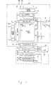
- the memory according to the embodiment is achieved by replacing the decoder 203 and the n-stage counter 204 in Fig. 1 by an m-stage access shift register 203', as shown in Fig. 3.
- the access shift register 203' has "m" shift stages and is controlled to shift the position of "1" output from the left side towards the right side in synchronism the signal SC2.
- the respective outputs (R -R m ) of the shift register 203' are applied to the bus line section 202 and used to selectively transfer one of the stages N -N m of the register 201 to the output circuit 206.
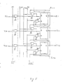
- bus line section 202 is shown in Fig. 4.
- the buffer section 202 includes "m" transfer gate transistors QY 1 -QY m receiving the outputs of the stages R i -R m of the shift register 203' at their gates, respectively and coupled between a data bus line DBL coupled to an input of the output circuit 206 and the outputs of the respective stages N 1 -N m of the line register 201.
- the "m" outputs of the column decoder 104 are applied to the shift register 203' via signal lines YL 1 -YL m and the switch circuit 205 to determine a start position of the shift register 203' in accordance with the output state of the column decoder 104.
- the decoder (203 in Fig. 1) is eliminated from the serial unit 200' by sharing the column decoder 104 in the RAM unit 100'. Therefore, the space for fabricating the serial unit 200' can be greatly reduced, and power consumption necessitated by the decoder 203 is also avoided.
- the signal lines YL l -YL m are formed in place of the signal lines connected between the address buffer 103 and the switching circuit 205 of Fig. 1, and it might be conceived that the number of the signal lines is relatively large.
- the signal lines YL -YL m can be formed by multilayer wiring technique and formed with overlap with transistors or other wirings.
- the increase in number of the signal lines YL, -YL m is not obstacle in increasing density of the memory.
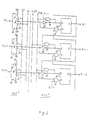
- the switching circuit 205' includes a plurality of AND gates such as 25, 26, 27 coupled the control signal DT and the signal lines YL ; -YL i-2 , respectively.
- the shift register 203' includes a plurality of flip-flops 34 - 36.
- a reset signal line RS is connected to reset terminals of the respective flip-flops via OR gates 31, 32, 33 which also receive the outputs of the succeeding stages, respectively.
- True and complementary shift signal lines SC2A and SC2B are coupled to inputs of AND gates 28, 29, 30 alternatively, as shown.
- the AND gates 28 - 30 also receive inputs coupled to the preceding stage outputs, respectively.
- the reset signal line RS is first set at a high level so that all the flip-flops are reset to be initialized. Then, the control line DT is raised to a high level so that the outputs (YL;, YL i+1 , YL i+2 ) of the column decoder 104 are applied to set terminals of the flip-flops so that only one of the flip-flops is set to produce "1" output with others "0" outputs. Then, "1" output state is shifted to the succeeding stage in response to active level of SC2A and SC2B one by one.
- the switch circuit 205' includes a plurality of CMOS gates each receiving one of the column decoder outputs YL ; , true and complementary control signals DT and DT .
- each of the CMOS gates operates as an inverter with respect to .its input e.g YL,.
- the levels of the respective inputs YL ; , YL i+1 , YL i+2 are inverted by the CMOS gates and applied to the reset terminals R of the respective flip-flops via the OR gates 31, 32.
Landscapes
- Engineering & Computer Science (AREA)
- Multimedia (AREA)
- Microelectronics & Electronic Packaging (AREA)
- Dram (AREA)
- Semiconductor Memories (AREA)
Applications Claiming Priority (2)
| Application Number | Priority Date | Filing Date | Title |
|---|---|---|---|
| JP61284811A JPS63136391A (ja) | 1986-11-27 | 1986-11-27 | 半導体メモリ装置 |
| JP284811/86 | 1986-11-27 |
Publications (2)
| Publication Number | Publication Date |
|---|---|
| EP0270028A2 true EP0270028A2 (fr) | 1988-06-08 |
| EP0270028A3 EP0270028A3 (fr) | 1990-06-06 |
Family
ID=17683316
Family Applications (1)
| Application Number | Title | Priority Date | Filing Date |
|---|---|---|---|
| EP87117590A Withdrawn EP0270028A3 (fr) | 1986-11-27 | 1987-11-27 | Dispositif de mémoire à double accès ayant un schéma d'accès séquentiel |
Country Status (3)
| Country | Link |
|---|---|
| US (1) | US4870621A (fr) |
| EP (1) | EP0270028A3 (fr) |
| JP (1) | JPS63136391A (fr) |
Cited By (1)
| Publication number | Priority date | Publication date | Assignee | Title |
|---|---|---|---|---|
| GB2260008A (en) * | 1991-09-12 | 1993-03-31 | Sony Corp | Multi port memory and digital interpolating apparatus |
Families Citing this family (18)
| Publication number | Priority date | Publication date | Assignee | Title |
|---|---|---|---|---|
| JPH0283899A (ja) * | 1988-09-20 | 1990-03-23 | Fujitsu Ltd | 半導体記憶装置 |
| US5150327A (en) * | 1988-10-31 | 1992-09-22 | Matsushita Electric Industrial Co., Ltd. | Semiconductor memory and video signal processing circuit having the same |
| DE69024086T2 (de) * | 1989-04-13 | 1996-06-20 | Sundisk Corp | EEprom-System mit Blocklöschung |
| US5257237A (en) * | 1989-05-16 | 1993-10-26 | International Business Machines Corporation | SAM data selection on dual-ported DRAM devices |
| US4985872A (en) * | 1989-06-23 | 1991-01-15 | Vlsi Technology, Inc. | Sequencing column select circuit for a random access memory |
| US5157775A (en) * | 1989-12-15 | 1992-10-20 | Eastman Kodak Company | Dual port, dual speed image memory access arrangement |
| JP3035995B2 (ja) * | 1990-06-29 | 2000-04-24 | ソニー株式会社 | マルチポートメモリ |
| US5257236A (en) * | 1991-08-01 | 1993-10-26 | Silicon Engineering, Inc. | Static RAM |
| KR960006284B1 (ko) * | 1991-10-03 | 1996-05-13 | 니뽄 덴끼 가부시끼가이샤 | 듀얼 포트 반도체 기억장치 |
| US5299159A (en) * | 1992-06-29 | 1994-03-29 | Texas Instruments Incorporated | Serial register stage arranged for connection with a single bitline |
| US5422998A (en) * | 1993-11-15 | 1995-06-06 | Margolin; Jed | Video memory with flash fill |
| GB2287627B (en) * | 1994-03-01 | 1998-07-15 | Vtech Electronics Ltd | Graphic video display system including graphic layers with sizable,positionable windows and programmable priority |
| US5526316A (en) * | 1994-04-29 | 1996-06-11 | Winbond Electronics Corp. | Serial access memory device |
| US6272465B1 (en) * | 1994-11-02 | 2001-08-07 | Legerity, Inc. | Monolithic PC audio circuit |
| US6167486A (en) | 1996-11-18 | 2000-12-26 | Nec Electronics, Inc. | Parallel access virtual channel memory system with cacheable channels |
| US6708254B2 (en) | 1999-11-10 | 2004-03-16 | Nec Electronics America, Inc. | Parallel access virtual channel memory system |
| JP4612139B2 (ja) * | 2000-02-08 | 2011-01-12 | 富士通セミコンダクター株式会社 | 入力回路及びその入力回路を利用する半導体装置 |
| CN102750986B (zh) | 2005-07-15 | 2015-02-11 | 夏普株式会社 | 信号输出电路、移位寄存器、输出信号生成方法、显示装置驱动电路和显示装置 |
Family Cites Families (3)
| Publication number | Priority date | Publication date | Assignee | Title |
|---|---|---|---|---|
| US4723226A (en) * | 1982-09-29 | 1988-02-02 | Texas Instruments Incorporated | Video display system using serial/parallel access memories |
| JPS6072020A (ja) * | 1983-09-29 | 1985-04-24 | Nec Corp | デュアルポ−トメモリ回路 |
| US4688197A (en) * | 1983-12-30 | 1987-08-18 | Texas Instruments Incorporated | Control of data access to memory for improved video system |
-
1986
- 1986-11-27 JP JP61284811A patent/JPS63136391A/ja active Pending
-
1987
- 1987-11-27 US US07/127,022 patent/US4870621A/en not_active Expired - Lifetime
- 1987-11-27 EP EP87117590A patent/EP0270028A3/fr not_active Withdrawn
Cited By (3)
| Publication number | Priority date | Publication date | Assignee | Title |
|---|---|---|---|---|
| GB2260008A (en) * | 1991-09-12 | 1993-03-31 | Sony Corp | Multi port memory and digital interpolating apparatus |
| US5418907A (en) * | 1991-09-12 | 1995-05-23 | Sony Corporation | Multi-port memory and digital interpolation apparatus |
| GB2260008B (en) * | 1991-09-12 | 1995-06-14 | Sony Corp | Multi port memory and digital interpolating apparatus |
Also Published As
| Publication number | Publication date |
|---|---|
| US4870621A (en) | 1989-09-26 |
| JPS63136391A (ja) | 1988-06-08 |
| EP0270028A3 (fr) | 1990-06-06 |
Similar Documents
| Publication | Publication Date | Title |
|---|---|---|
| EP0135940B1 (fr) | Circuit de mémoire à double porte | |
| US4870621A (en) | Dual port memory device with improved serial access scheme | |
| US4855959A (en) | Dual port memory circuit | |
| EP0069764B1 (fr) | Systeme de memoire a acces selectif ayant des chemins de circulation de donnees serielles a haute vitesse | |
| US4541075A (en) | Random access memory having a second input/output port | |
| US4899316A (en) | Semiconductor memory device having serial writing scheme | |
| US4648077A (en) | Video serial accessed memory with midline load | |
| US4683555A (en) | Serial accessed semiconductor memory with reconfigureable shift registers | |
| US4667313A (en) | Serially accessed semiconductor memory with tapped shift register | |
| US4686650A (en) | Monolithic storage device | |
| US20030206480A1 (en) | Semiconductor memory device | |
| EP0523759B1 (fr) | Mémoire à semi-conducteur à accès en série | |
| JPH0636311B2 (ja) | 2重ポートvramメモリ | |
| US4611299A (en) | Monolithic storage device | |
| US4811305A (en) | Semiconductor memory having high-speed serial access scheme | |
| US5317540A (en) | Semiconductor memory device | |
| US4951251A (en) | Semiconductor memory device | |
| JPS61288240A (ja) | 半導体記憶装置 | |
| WO1985002935A1 (fr) | Dispositif a memoire a semi-conducteur pour applications de balayage seriel | |
| US4841567A (en) | Memory device | |
| US4710896A (en) | Semiconductor memory having multiple access | |
| KR970005411B1 (ko) | 선택적인 행 기입 능력을 가진 판독/기입 메모리 및 이러한 메모리에 테이타를 기입하는 방법 | |
| US6445634B2 (en) | Serial access memory and data write/read method | |
| KR920005121B1 (ko) | 반도체 기억장치 | |
| JP3160930B2 (ja) | 半導体記憶装置の読み出し回路 |
Legal Events
| Date | Code | Title | Description |
|---|---|---|---|
| PUAI | Public reference made under article 153(3) epc to a published international application that has entered the european phase |
Free format text: ORIGINAL CODE: 0009012 |
|
| 17P | Request for examination filed |
Effective date: 19871127 |
|
| AK | Designated contracting states |
Kind code of ref document: A2 Designated state(s): DE FR GB |
|
| PUAL | Search report despatched |
Free format text: ORIGINAL CODE: 0009013 |
|
| AK | Designated contracting states |
Kind code of ref document: A3 Designated state(s): DE FR GB |
|
| 17Q | First examination report despatched |
Effective date: 19911010 |
|
| STAA | Information on the status of an ep patent application or granted ep patent |
Free format text: STATUS: THE APPLICATION HAS BEEN WITHDRAWN |
|
| 18W | Application withdrawn |
Withdrawal date: 19920212 |
|
| RIN1 | Information on inventor provided before grant (corrected) |
Inventor name: NAKADA, KAZUHIRO |