EP0272106A2 - Circuit de réglage de gain avec un déphasage constant - Google Patents
Circuit de réglage de gain avec un déphasage constant Download PDFInfo
- Publication number
- EP0272106A2 EP0272106A2 EP87311090A EP87311090A EP0272106A2 EP 0272106 A2 EP0272106 A2 EP 0272106A2 EP 87311090 A EP87311090 A EP 87311090A EP 87311090 A EP87311090 A EP 87311090A EP 0272106 A2 EP0272106 A2 EP 0272106A2
- Authority
- EP
- European Patent Office
- Prior art keywords
- gain control
- control circuit
- voltage
- set forth
- coupled
- Prior art date
- Legal status (The legal status is an assumption and is not a legal conclusion. Google has not performed a legal analysis and makes no representation as to the accuracy of the status listed.)
- Withdrawn
Links
- 230000009977 dual effect Effects 0.000 claims abstract description 23
- 239000004065 semiconductor Substances 0.000 claims 3
- 238000013459 approach Methods 0.000 description 4
- 238000000034 method Methods 0.000 description 4
- 230000005540 biological transmission Effects 0.000 description 3
- 230000009021 linear effect Effects 0.000 description 3
- 238000004458 analytical method Methods 0.000 description 2
- 230000008859 change Effects 0.000 description 2
- 238000011161 development Methods 0.000 description 2
- 238000004519 manufacturing process Methods 0.000 description 2
- 238000012986 modification Methods 0.000 description 2
- 230000004048 modification Effects 0.000 description 2
- 230000008569 process Effects 0.000 description 2
- 230000009467 reduction Effects 0.000 description 2
- 238000012552 review Methods 0.000 description 2
- 229910001218 Gallium arsenide Inorganic materials 0.000 description 1
- 230000008878 coupling Effects 0.000 description 1
- 238000010168 coupling process Methods 0.000 description 1
- 238000005859 coupling reaction Methods 0.000 description 1
- 238000010586 diagram Methods 0.000 description 1
- 230000000694 effects Effects 0.000 description 1
- 238000005516 engineering process Methods 0.000 description 1
- 230000005669 field effect Effects 0.000 description 1
- 238000002955 isolation Methods 0.000 description 1
- 238000005259 measurement Methods 0.000 description 1
- 238000012545 processing Methods 0.000 description 1
- 238000011160 research Methods 0.000 description 1
- 229920006395 saturated elastomer Polymers 0.000 description 1
Images
Classifications
-
- H—ELECTRICITY
- H03—ELECTRONIC CIRCUITRY
- H03G—CONTROL OF AMPLIFICATION
- H03G1/00—Details of arrangements for controlling amplification
- H03G1/0005—Circuits characterised by the type of controlling devices operated by a controlling current or voltage signal
- H03G1/0035—Circuits characterised by the type of controlling devices operated by a controlling current or voltage signal using continuously variable impedance elements
- H03G1/007—Circuits characterised by the type of controlling devices operated by a controlling current or voltage signal using continuously variable impedance elements using field-effect transistors [FET]
Definitions
- This invention relates to a constant phase gain control circuit for use in conjunction with a dual gate field effect transistor (FET) in constant phase variable power amplifier applications.
- FET field effect transistor
- Phased array radar systems are being increasingly utilized in the military electronics industry. Many such systems are presently under development as evidenced by the articles "A Dual-Gate FET Constant Phase Variable Power Amplifier,” of D. M. Drury, D. C. Zimmermann and D. E. Zimmerman, 1985 IEEE MTT-S International Microwave Symposium Digest, "Class-B Operation of Microwave FETs for Array Module Applications,”, of M. Cohn, J. E. Degenford and R. G. Freitag, 1982 IEEE MTT-S International Microwave Symposium Digest and "High Efficiency Single-ended and Push-pull Class-B FET Power Amplifiers," of R. G. Freitag, J. E. Degenford and M. Cohn, 1985 Government Microcircuit Applications Conference. These systems require extremely small module packages. These systems require the extensive use of microwave monolithic integrated circuits (MMICs) as the active elements in the module. A particular element in these systems which has been the topic of much research is the constant phase variable power amplifier (VPA).
- MMICs microwave
- Another approach which is presently under development in airborne phased array power amplifiers is the use of dual gate devices to implement power programmability.
- One inherent need in such applications is the ability to provide power programmability with a low phase error or phase change over the programmable region.
- One approach is a monolithic variable power amplifier (VPA) which uses dual gate FETs.
- the dual gate FETs are configured with an rf termination on the second gate of the dual gate FET, chosen for optimum phase performance on the second gate of the FET.
- Dual gate FETs configured in this way have been modelled as two single gate FETs connected in cascode. Sec, for example, the above noted Drury et al.
- variable power feature is achieved by changing the bias applied to the second gate.
- VSWR voltage standing wave ratio
- variable power amplifiers have implemented the variable power mode by changing the bias applied to gate-2 of the dual gate FET exclusively as demonstrated in the above noted Drury et al. article. Since these devices operate in the saturated regime, there are elements in the FET equivalent circuit which are nonlinear in nature.
- each resistor R1 and R2 can be segmented in a monolithic implementation such that several different slopes and/or offsets can be achieved by selective wire bonding of the segmented resistor on the chip after processing.
- Vg1 the value of Vg1 was varied less than twenty percent, resulting in essentially no change of the device input impedance. Therefore, this control circuit will not cause appreciable variation of the input VSWR which could result in phase errors.
- the constant phase Vg1 f(Vg2) gain control circuit significantly simplifies the task of realizing constant phase variable power amplifiers which meet the system level phase variation requirements.
- the power amplifier circuit comprises a dual gate FET of the type used in the prior art wherein a d-c bias is applied to gate electrode G1 of the FET with a variable voltage being placed on gate electrode G2 thereof to implement the gain control. Power programmability is altered by making one of the potentials a function of the other.
- An offset voltage is applied at one node which is effectively similar to the gate G1 node of the prior art and the gain control voltage Vgc which is variable, as in the prior art, is applied to the other node.
- the two voltages at gates G1 and G2 are made functions of each other by coupling the gates G1 and G2 of the dual gate transistor with a resistor R1 of the FIGURE and placing a resistor R2 of the FIGURE in the offset voltage line.
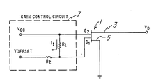
- the FIGURE is a circuit diagram of a constant phase gain control circuit connected to a dual gate FET in accordance with the present invention.
- FIG. 1 there is shown a prior art dual gate FET 1 having a drain electrode 3 coupled to a circuit output Vd.
- the other source electrode 5 thereof is coupled to reference voltage or ground.
- the FET also includes a first gate electrode G1 and a second gate electrode G2.
- a gain control circuit 7 is connected to the gate electrodes of the FET 1, the gain control circuit including a Voffset input, which is a constant d-c input voltage, coupled through a resistor R2 to the gate electrode G1, a Vgc input coupled to the gate electrode G2 and a resistor R1 coupled between the gate electrode G2 and the gate electrode G1.
- the values of the resistors are determined empirically as will be explained hereinbelow.
Landscapes
- Amplifiers (AREA)
- Control Of Amplification And Gain Control (AREA)
- Networks Using Active Elements (AREA)
Applications Claiming Priority (2)
| Application Number | Priority Date | Filing Date | Title |
|---|---|---|---|
| US943272 | 1986-12-17 | ||
| US06/943,272 US4870373A (en) | 1986-12-17 | 1986-12-17 | Constant phase gain control circuit |
Publications (2)
| Publication Number | Publication Date |
|---|---|
| EP0272106A2 true EP0272106A2 (fr) | 1988-06-22 |
| EP0272106A3 EP0272106A3 (fr) | 1990-10-10 |
Family
ID=25479350
Family Applications (1)
| Application Number | Title | Priority Date | Filing Date |
|---|---|---|---|
| EP19870311090 Withdrawn EP0272106A3 (fr) | 1986-12-17 | 1987-12-16 | Circuit de réglage de gain avec un déphasage constant |
Country Status (3)
| Country | Link |
|---|---|
| US (1) | US4870373A (fr) |
| EP (1) | EP0272106A3 (fr) |
| JP (1) | JPS63232608A (fr) |
Cited By (1)
| Publication number | Priority date | Publication date | Assignee | Title |
|---|---|---|---|---|
| FR2652461A1 (fr) * | 1989-09-26 | 1991-03-29 | Alcatel Espace | Attenuateur a transistor a effet de champ bigrille. |
Families Citing this family (2)
| Publication number | Priority date | Publication date | Assignee | Title |
|---|---|---|---|---|
| JP4269542B2 (ja) * | 2001-06-04 | 2009-05-27 | 日本電気株式会社 | トランジスタの動作点設定方法及びその回路、信号成分値変更方法並びにアクティブマトリクス型液晶表示装置 |
| US9531086B1 (en) * | 2016-01-06 | 2016-12-27 | International Business Machines Corporation | Dynamic phased array tapering without phase recalibration |
Family Cites Families (9)
| Publication number | Priority date | Publication date | Assignee | Title |
|---|---|---|---|---|
| US3480873A (en) * | 1967-12-11 | 1969-11-25 | Rca Corp | Gain control biasing circuits for field-effect transistors |
| JPS4841382A (fr) * | 1971-09-28 | 1973-06-16 | ||
| JPS5180743A (fr) * | 1975-01-13 | 1976-07-14 | Onkyo Kk | |
| DE2833056C3 (de) * | 1978-07-27 | 1984-02-16 | Texas Instruments Deutschland Gmbh, 8050 Freising | HF-Verstärker |
| DE2911514C2 (de) * | 1979-03-23 | 1982-07-15 | Texas Instruments Deutschland Gmbh, 8050 Freising | HF-Verstärkerschaltung |
| JPS58156208A (ja) * | 1982-03-11 | 1983-09-17 | Clarion Co Ltd | 自動リニアリテイ補正回路 |
| GB2117583B (en) * | 1982-03-31 | 1986-01-29 | Ferranti Plc | Gain control circuit |
| US4468631A (en) * | 1982-05-24 | 1984-08-28 | Rca Corporation | Amplitude control apparatus |
| JPS618965A (ja) * | 1984-06-22 | 1986-01-16 | Nec Kansai Ltd | 半導体装置の製造方法 |
-
1986
- 1986-12-17 US US06/943,272 patent/US4870373A/en not_active Expired - Lifetime
-
1987
- 1987-12-16 EP EP19870311090 patent/EP0272106A3/fr not_active Withdrawn
- 1987-12-17 JP JP62320057A patent/JPS63232608A/ja active Pending
Cited By (3)
| Publication number | Priority date | Publication date | Assignee | Title |
|---|---|---|---|---|
| FR2652461A1 (fr) * | 1989-09-26 | 1991-03-29 | Alcatel Espace | Attenuateur a transistor a effet de champ bigrille. |
| EP0420106A1 (fr) * | 1989-09-26 | 1991-04-03 | Alcatel Espace | Atténuateur à transistor à effet de champ bigrille |
| US5151669A (en) * | 1989-09-26 | 1992-09-29 | Alcatel Espace | Dual-gate fet attenuator controlled by a variable load circuit |
Also Published As
| Publication number | Publication date |
|---|---|
| EP0272106A3 (fr) | 1990-10-10 |
| JPS63232608A (ja) | 1988-09-28 |
| US4870373A (en) | 1989-09-26 |
Similar Documents
| Publication | Publication Date | Title |
|---|---|---|
| US5028879A (en) | Compensation of the gate loading loss for travelling wave power amplifiers | |
| US4875023A (en) | Variable attenuator having voltage variable FET resistor with chosen resistance-voltage relationship | |
| US4975604A (en) | Automatic return-loss optimization of a variable fet attenuator | |
| EP0606094A2 (fr) | Circuit intégré monolithique à micro-ondes | |
| US4525678A (en) | Monolithic low noise common-gate amplifier | |
| US6316997B1 (en) | CMOS amplifiers with multiple gain setting control | |
| US6188279B1 (en) | Low cost miniature broadband linearizer | |
| JP3594775B2 (ja) | 電力増幅器 | |
| US4870373A (en) | Constant phase gain control circuit | |
| US4908531A (en) | Monolithic active isolator | |
| US4912430A (en) | Current source as a microwave biasing element | |
| US6734712B2 (en) | Logarithmic amplifier | |
| Ayasli et al. | 2-20-GHz GaAs traveling-wave amplifier | |
| EP0250453B1 (fr) | Amplificateur en cascade dependant de l'impedance interne et pourvu d'une commande de gain variable de precision | |
| EP0367330B1 (fr) | Circuit amplificateur à amplification linéaire | |
| US6400222B1 (en) | Linearizer | |
| US6774416B2 (en) | Small area cascode FET structure operating at mm-wave frequencies | |
| JPH02279013A (ja) | アイソレータ回路からなる集積半導体装置 | |
| JP2771170B2 (ja) | 可変減衰装置 | |
| EP0101174B1 (fr) | Amplificateur monolithique à faible bruit à transistor à effet de champ avec montage à grille commune | |
| JP2959004B2 (ja) | 半導体集積回路 | |
| JPH0562844B2 (fr) | ||
| JPH03238910A (ja) | アッテネータ | |
| US5338989A (en) | Microwave integrated circuit | |
| US4890068A (en) | Open-loop current amplifiers having improved gain characteristics |
Legal Events
| Date | Code | Title | Description |
|---|---|---|---|
| PUAI | Public reference made under article 153(3) epc to a published international application that has entered the european phase |
Free format text: ORIGINAL CODE: 0009012 |
|
| AK | Designated contracting states |
Kind code of ref document: A2 Designated state(s): DE FR IT |
|
| PUAL | Search report despatched |
Free format text: ORIGINAL CODE: 0009013 |
|
| AK | Designated contracting states |
Kind code of ref document: A3 Designated state(s): DE FR IT |
|
| STAA | Information on the status of an ep patent application or granted ep patent |
Free format text: STATUS: THE APPLICATION IS DEEMED TO BE WITHDRAWN |
|
| 18D | Application deemed to be withdrawn |
Effective date: 19910411 |