EP0272885B1 - Dispositif semi-conducteur comportant une diode de décalage de niveau - Google Patents
Dispositif semi-conducteur comportant une diode de décalage de niveau Download PDFInfo
- Publication number
- EP0272885B1 EP0272885B1 EP87311148A EP87311148A EP0272885B1 EP 0272885 B1 EP0272885 B1 EP 0272885B1 EP 87311148 A EP87311148 A EP 87311148A EP 87311148 A EP87311148 A EP 87311148A EP 0272885 B1 EP0272885 B1 EP 0272885B1
- Authority
- EP
- European Patent Office
- Prior art keywords
- layer
- level shift
- diodes
- semiconductor device
- diode
- Prior art date
- Legal status (The legal status is an assumption and is not a legal conclusion. Google has not performed a legal analysis and makes no representation as to the accuracy of the status listed.)
- Expired - Lifetime
Links
Images



Classifications
-
- H—ELECTRICITY
- H10—SEMICONDUCTOR DEVICES; ELECTRIC SOLID-STATE DEVICES NOT OTHERWISE PROVIDED FOR
- H10D—INORGANIC ELECTRIC SEMICONDUCTOR DEVICES
- H10D8/00—Diodes
- H10D8/825—Diodes having bulk potential barriers, e.g. Camel diodes, planar doped barrier diodes or graded bandgap diodes
-
- H—ELECTRICITY
- H10—SEMICONDUCTOR DEVICES; ELECTRIC SOLID-STATE DEVICES NOT OTHERWISE PROVIDED FOR
- H10D—INORGANIC ELECTRIC SEMICONDUCTOR DEVICES
- H10D84/00—Integrated devices formed in or on semiconductor substrates that comprise only semiconducting layers, e.g. on Si wafers or on GaAs-on-Si wafers
- H10D84/01—Manufacture or treatment
-
- H—ELECTRICITY
- H10—SEMICONDUCTOR DEVICES; ELECTRIC SOLID-STATE DEVICES NOT OTHERWISE PROVIDED FOR
- H10D—INORGANIC ELECTRIC SEMICONDUCTOR DEVICES
- H10D84/00—Integrated devices formed in or on semiconductor substrates that comprise only semiconducting layers, e.g. on Si wafers or on GaAs-on-Si wafers
- H10D84/01—Manufacture or treatment
- H10D84/02—Manufacture or treatment characterised by using material-based technologies
- H10D84/05—Manufacture or treatment characterised by using material-based technologies using Group III-V technology
Definitions
- the present invention generally relates to semiconductor devices having level shift diodes with an arbitrary level shift quantity by utilizing a discontinuity in the energy band at a heterojunction between two semiconductors.
- a level shift diode is constructed by utilizing the fact that a forward voltage drop is approximately constant at a pn junction.
- the level shift diode is used to shift a voltage level by a predetermined value in a logic circuit and the like employing transistors.
- a voltage drop introduced by one pn junction is insufficient, a plurality of level shift diodes are connected in series according to the needs.
- a level shift quantity of a level shift diode utilizing a Schottky junction is a constant value which is approximately in a range of 0.6 V to 0.8 V per Schottky junction, because the Schottky barrier height is in the range of 0.6 V to 0.8 V regardless of the kind of metal formed on the GaAs layer.
- the Schottky junction is made by forming a metal layer on the GaAs substrate.
- the surface of the GaAs substrate is exposed to the air when forming the metal layer thereon.
- the surface of the GaAs substrate includes irregularities when compared to that of the silicon substrate, and for this reason, it is difficult to accurately control the level shift quantity of the Schottky diode because the Schottky diode is easily affected by a leakage current.
- a large area of the semiconductor device is occupied by the Schottky diodes for providing the desired level shift.
- the diode is a Schottky diode in series with the gate of the FET.
- US-A-4 353 081 discloses a semiconductor diode having a GaAs/AlGaAs heterojunction, employing a graded composition to provide control over the shape of the potential barrier. A series arrangement of such diodes is also disclosed, in accordance with the preamble of accompanying claim 1.
- a semiconductor device comprising a substrate and at least two level shift diodes provided on said substrate, said diodes having a stacked structure comprising:- a first layer of a first compound semiconductor having a first electron affinity; a second layer of a second compound semiconductor formed on said first layer and having a second electron affinity less than said first electron affinity, forming a first heterojunction between said first and second layers, said first and second compound semiconductors being any arbitrary combination of n-type and i-type semiconductors; a third layer comprising said first compound semiconductor with the first electron affinity and formed on said second layer; at least one fourth layer of similar composition to said second layer, formed on said third layer; a first electrode formed on said first layer; and a second electrode formed on said third layer; characterised in that:- at least one field effect transistor is provided on said substrate whereby at least a portion of said first layer (74a) is used in common with said field effect transistor as a layer of said field effect transistor and as a layer of said diodes,
- the level shift quantity it is possible to arbitrarily set the level shift quantity by stacking a plurality of heteroiunctions and by appropriately changing the composition of the compound semiconductor heterojunction forming layer constituting the heterojunction which generates a discontinuity in the energy band.
- the area of the level shift diodes on the semiconductor device is small compared to that of a Schottky diode.
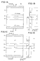
- FIG. 1A shows a level shift diode which is useful for explaining the semiconductor device according to the present invention.
- a level shift diode 10 comprises an n+-type gallium arsenide (GaAs) anode contact layer 11, an n-type GaAs heterojunction forming layer 12, an n-type (or i-type) aluminum gallium arsenide (AlGaAs) heterojunction forming layer 13, an n+-type AlGaAs cathode contact layer 14, an anode electrode 15, and a cathode electrode 16.
- GaAs gallium arsenide
- AlGaAs aluminum gallium arsenide
- FIG.1B shows an energy band diagram of the level shift diode 10.
- E c denotes the bottom of the conduction band
- ⁇ E a denotes the barrier height at the energy band gap produced by the difference in the electron affinities of the n-type GaAs heterojunction forming layer 12 and the n-type AlGaAs heterojunction forming layer 13.
- a barrier height E B becomes small and a current starts to flow when a positive voltage is applied to the anode electrode 15, a negative voltage is applied to the cathode electrode 16 and the two voltages are increased.
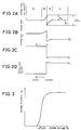
- FIGS.2A through 2C show the energy band diagram of the level shift diode 10 for different anode voltages V a
- FIG.3 shows the anode voltage V a versus anode current I a characteristic of the level shift diode 10.
- FIGS.2A through 2C and 3 those parts which are the same as those corresponding parts in FIGS.1A and 1B are designated by the same reference numerals and characters.
- the barrier height ⁇ E a is sufficiently high, and no anode current I a flows.
- FIG.2B shows the energy band diagram for the case where V a ⁇ ⁇ E a /e, where e denotes the electronic charge.
- the barrier height ⁇ E a decreases compared to the case shown in FIG.2A, and a slight anode current I a starts to flow.
- FIG.2C shows the energy band diagram for the case where V a ⁇ ⁇ E a /e.
- the barrier height ⁇ E a decreases even further from the case shown in FIG.2B, and a large anode current I a flows thereby reaching saturation.
- the level (voltage) shift quantity changes depending on the barrier height ⁇ E a at the heterojunction interface.
- the barrier height ⁇ E a can be varied by changing the composition of the n-type AlGaAs heterojunction forming layer 13 which is one of the semiconductor layers for forming the heterojunction interface, that is, by varying Al content x of Al x Ga 1-x As which constitutes the n-type AlGaAs heterojunction forming layer 13.
- the level shift quantity of the level shift diode 10 can be changed continuously by appropriately varying the Al content x of Al x Ga 1-x As. Furthermore, it is possible to more accurately control the level shift quantity compared to the Schottky diode.
- FIG.1C shows a level shift diode with p-type semiconductors in which the carriers are holes.
- FIG.1D is an energy band diagram of the level shift diode in FIG.1C.
- E v denotes the bottom of the valence band
- E barrier denotes the barrier height at the energy band gap produced by the difference in the energy level of the valence band for the holes.
- the energy level of E v in the first layer 12 is higher than that of the second layer 13 at the heterojunction.
- FIG.2D shows the energy band diagram for the case where V a ⁇ ⁇ E barrier /e. In this case, holes are injected from the anode to the cathode.
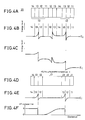
- FIG.4A shows another level shift diode which is useful for explaining the present invention.
- a level shift diode 20 essentially comprises two level shift diodes 10 which are connected in series.
- FIG.5 shows an anode voltage V a versus anode current I a characteristic of the level shift diode 20.
- FIGS.4A through 4C and 5 those parts which are the same as those corresponding parts in FIGS.1A and 1B are designated by the same reference numerals and characters.
- the two level shift diodes 10 constituting the level shift diode 20 are identical both in construction and characteristic.
- the two level shift diodes 10 may have the same construction but different barrier heights ⁇ E a .
- the Al content x of the Al x Ga 1-x As which constitutes the n-type AlGaAs heterojunction forming layer 13 of one of the two level shift diodes 10 may be different from that of the other of the two level shift diodes 10.
- the level (voltage) shift quantity of the level shift diode 20 it is easier to control the level (voltage) shift quantity of the level shift diode 20 to a desired value than simply controlling to the same value the Al content x of the Al x Ga 1-x As which constitutes the n-type AlGaAs heterojunction forming layer 13 of the two level shift diodes 10 having identical construction and characteristic.
- FIG.4D shows the level shift diode which has a Al x Ga 1-x As layer 17 with graded composition x in substitute of the layers 11 through 14 in FIG.4A.
- FIG.4E shows the energy band diagram of the level shift diode of FIG.4D in which the energy level of the conduction band in the layer 17 changes gradually.
- FIG.4F shows Al composition of FIGS.4D and 4E.
- FIG.6 is a circuit diagram of the device.
- the semiconductor device is a buffered field effect transistor logic (BFL) circuit comprising transistors Q1 through Q4 and a level shift diode D1.
- IN and OUT respectively denote input and output terminals, V DD denotes a positive power source voltage, and V SS denotes a negative power source voltage.
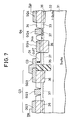
- FIG.7 shows an essential part of the device indicated by a phantom line in FIG.6.
- those parts which are the same as those corresponding parts in FIG.6 are designated by the same reference numerals and characters.
- the semiconductor device comprises a semiinsulating GaAs substrate 31, an undoped (intrinsic) GaAs active layer 32, an n+-type AlGaAs electron supplying layer 33, a level shift diode region 34, an element isolation region 35, alloyed regions 36, a two dimensional electron gas (2DEG) layer 37, source electrodes SQ3 and SQ4, drain electrodes DQ3 and DQ4, gate electrodes GQ3 and GQ4, and a cathode electrode CD of the level shift diode D1.
- High electron mobility transistors HEMTs are used for the transistors Q3 and Q4.
- FIG.8 shows on an enlarged scale the level shift diode region 34 shown in FIG.7 together with the n+-type AlGaAs electron supplying layer 33.
- the level shift diode region 34 comprises an n+-type GaAs layer 34A, an n-type GaAs layer 34B, an n-type AlGaAs layer 34C, an n+-type AlGaAs layer 34D, an n-type AlGaAs layer 34C, an n-type GaAs layer 34B, an n+-type GaAs layer 34A, an n-type GaAs layer 34B, an n-type AlGaAs layer 34C, and an n -type AlGaAs layer 34D.
- the n+-type AlGaAs electron supplying layer 33 and the level shift diode region 34 constitute the level shift diode D1 which is essentially the same as the level shift diode 20 described before in conjunction with FIGS.4A through 4C and 5.
- the drain electrode DQ4 functions as the anode electrode of the level shift diode D1.
- the level shift diode region 34 comprises highly doped layers, the level shift diode region 34 can also function satisfactorily as an electrode contact layer.
- the level shift diode D1 is connected between the source electrode SQ3 of the transistor Q3 and the drain electrode DQ4 of the transistor Q4, and the semiconductor device shown in FIG.7 is identical to the essential part of the BFL circuit indicated by the phantom lines in FIG.6.
- FIG.9 shows an essential part of a modification of the device in Fig. 6.
- those parts which are the same as those corresponding parts in FIGS.7 and 8 are designated by the same reference numerals, and a description thereof will be omitted.
- One n-type GaAs layer 34B and one n-type AlGaAs layer 34C respectively in the middle are omitted from the level shift diode region 34 shown in FIG.8.
- an alloyed region 39 is formed in the top n+-type AlGaAs layer 34D.
- these omitted layers 34B and 34C have little effect and are omitted in this modification for this reason.
- the illustration of the connection between the cathode electrode CD and the source electrode SQ3 is omitted in FIG.9.
- FIGS.7 through 9 and FIGS.11, 12, 14 and 15 which will be described later, the symbols of the diode and/or transistor are shown in the cross sectional view to facilitate the understanding thereof.
- FIG.10 is a circuit diagram of the second device.
- the semiconductor device is a Schottky diode field effect transistor logic (SDFL) circuit comprising transistors Q11 through Q13 and a level shift diode D2.
- IN and OUT respectively denote input and output terminals, V DD denotes a positive power source voltage, and -V SS denotes a negative power source voltage.
- SDFL Schottky diode field effect transistor logic
- FIG.11 shows an essential part of the second device.
- those parts which are the same as those corresponding parts in FIG.10 are designated by the same reference numerals and characters.
- the semiconductor device comprises a semiinsulating GaAs substrate 51, an undoped (intrinsic) GaAs active layer 52, an n+-type AlGaAs electron supplying layer 53, a GaAs layer 54, an element isolation region 55, alloyed regions 56, a two dimensional electron gas (2DEG) layer 57, a level shift diode region 58, source electrodes SQ11, SQ12 and SQ13, drain electrodes DQ11, DQ12 and DQ13, gate electrodes GQ11, GQ12 and GQ13, and a cathode electrode CD of the level shift diode D2.
- 2DEG two dimensional electron gas
- the GaAs layer 54 is made up of an n+-type GaAs layer 54a and an n-type GaAs layer 54b.
- the level shift diode region 58 comprises an AlGaAs layer 61, an GaAs layer 62 and an AlGaAs layer 63.
- HEMTs are used for the transistors Q11 through Q13.
- the AlGaAs layer 61 comprises an n-type AlGaAs layer 61a, an n+-type AlGaAs layer 61b and an n-type AlGaAs layer 61c.
- the GaAs layer 62 comprises an n-type GaAs layer 62a, an n+-type GaAs layer 62b and an n-type GaAs layer 62c.
- the AlGaAs layer 63 comprises an n-type-AlGaAs layer 63a and an n+-type AlGaAs layer 63b.
- the level shift diode D2 is connected between the cathode electrode CD and the drain electrode DQ11 of the transistor Q11, and the semiconductor device shown in FIG.11 is identical to the SDFL circuit shown in FIG. 10.
- FIG.13 is a circuit diagram of the embodiment.
- the semiconductor device is a field effect transistor logic with Schottky diode and coupling capacitor (FLSC) circuit comprising transistors Q21 and Q22, level shift diodes D3 and D4 and a resistor R.
- IN and OUT respectively denote input and output terminals
- V DD denotes a positive power source voltage
- -V SS denotes a negative power source voltage.
- FIG.14 shows an essential part of the embodiment.
- those parts which are the same as those corresponding parts in FIG.13 are designated by the same reference numerals and characters.
- the semiconductor device comprises a semiinsulating GaAs substrate 71, an undoped GaAs active layer 72, an n+-type AlGaAs electron supplying layer 73, a GaAs layer 74, an element isolation region 75, alloyed regions 76, a two dimensional electron gas (2DEG) layer 77, level shift diode regions 78 and 79, a source electrode SQ22, a drain electrode DQ22, a gate electrode GQ22, an anode electrode AD of the level shift diode D4, and a cathode electrode CD of the level shift diode D3.
- 2DEG two dimensional electron gas
- the GaAs layer 74 is made up of an n+-type GaAs layer 74a and n-type GaAs layer 74b.
- the level shift diode region 78 comprises an AlGaAs layer 81, a GaAs layer 82 and an AlGaAs layer 83.
- the level shift diode region 79 comprises the AlGaAs layer 81 and the GaAs layer 82.
- HEMTs are used for the transistors Q21 and Q22.
- the AlGaAs layer 81 comprises an n-type AlGaAs layer 81a, an n+-type AlGaAs layer 81b and an n-type AlGaAs layer 81c.
- the GaAs layer 82 comprises an n-type GaAs layer 82a, an n -type GaAs layer 82b and an n-type GaAs layer 82c.
- the AlGaAs layer 83 comprises an n-type AlGaAs layer 83a and an n+-type AlGaAs layer 83b.
- the level shift diodes D3 and D4 are connected in parallel, and the semiconductor device shown in FIG.13 is identical to the essential part of the FLSC circuit shown in FIG. 14.
- the level shift quantity of the level shift diode in the semiconductor device is accurately controlled to a desired value because the level shift diode utilizes the heterojunction.
- the level shift diode only occupies a small area on the semiconductor device compared to the conventional semiconductor using a Schottky diode.
- n+-type GaAs layer after a plurality of the n+-type GaAs layer, the n-type GaAs layer, the n-type AlGaAs layer and the n+-type AlGaAs layer are stacked, it is possible to form a plurality of level shift diodes on the same substrate by isolating level shift diode regions and removing a predetermined number of layers from arbitrary ones of the level shift diode regions. In this manner, it is possible to form level shift diodes coupled in opposite directions on the same substrate, by simply making the number of layers of the level shift diode regions different from each other.
- the level shift diode at least comprises a first layer made of a first compound semiconductor and a second layer made of a second compound semiconductor having an electron affinity smaller than that of the first compound semiconductor, where the first and second compound semiconductors are both made of n-type semiconductors.
- the first and second compound semiconductors may both be made of either one of n-type and i-type semiconductors.
- the first and second compound semiconductors may both be made of either one of p-type and i-type semiconductors. It will be readily apparent to those skilled in the art that the described embodiment may be modified to suit the case where the first and second compound semiconductors are both made of either one of p-type and i-type semiconductors, for example.
Landscapes
- Junction Field-Effect Transistors (AREA)
Claims (7)
- Dispositif semi-conducteur comprenant un substrat (71, 72, 73) et au moins deux diodes de décalage de niveau (D3, D4) placées sur ledit substrat, lesdites diodes ayant une structure empilée comprenant :
une première couche (74a, 74b) d'un premier semi-conducteur composé ayant une première affinité d'électrons ;
une seconde couche (81) d'un second semiconducteur composé formé sur ladite première couche et ayant une seconde affinité d'électrons inférieure à ladite première affinité d'électrons, formant une première jonction hétérogène entre lesdites première et seconde couches, lesdits premier et second semi-conducteurs composés étant une combinaison arbitraire de semi-conducteurs de type n et de type i ;
une troisième couche (82) comprenant ledit premier semi-conducteur composé avec la première affinité d'électrons et formé sur ladite seconde couche (81) ;
au moins une quatrième couche (83) de composition similaire à ladite seconde couche, formée sur ladite troisième couche ;
une première électrode formée sur ladite première couche (74a, 74b) ; et
une seconde électrode (AD) formée sur ladite troisième couche (82) ;
caractérisé en ce que :
au moins un transistor à effet de champ (Q22) est placé sur ledit substrat grâce auquel au moins une partie de ladite première couche (74a) est utilisée en commun avec ledit transistor à effet de champ comme couche dudit transistor à effet de champ et comme couche desdites diodes, et lesdites diodes (D3, D4) sont des diodes de décalage de niveau dans lesquelles ladite troisième couche (82) forme une seconde jonction hétérogène avec ladite seconde couche (81) ; et
lesdites couches de la seconde à la quatrième sont formées sélectivement sur une pluralité de positions mutuellement isolées sur ledit substrat, grâce auquel sur une première position une première diode (D4) desdites diodes de décalage de niveau (D3, D4) est formée qui comprend ladite seconde couche (81) et ladite troisième couche (82) et sur une seconde position une seconde diode (D3) desdites diodes de décalage de niveau (D3, D4) est formée qui comprend ladite seconde couche (81), ladite troisième couche (82) et ladite quatrième couche, lesdites diodes de décalage de niveau (D3, D4) ayant des directions de polarisation mutuellement opposées. - Dispositif semi-conducteur selon la revendication 1, dans lequel ledit premier semiconducteur composé est de l'arséniure de gallium (GaAs) et ledit second semi-conducteur composé est de l'arséniure de gallium aluminium (AlGaAs).
- Dispositif semi-conducteur selon la revendication 1, dans lequel ledit premier semiconducteur composé est de l'arséniure de gallium (GaAs) et ledit second semi-conducteur composé est de l'arséniure de gallium aluminium AlxGa1-xAs, lesdites diodes de décalage de niveau (D3, D4) ayant des valeurs de décalage de niveau déterminées par la teneur x en aluminium.
- Dispositif semi-conducteur selon l'une quelconque des revendications précédentes, dans lequel une composition dudit second semi-conducteur composé est sélectionnée de telle sorte que lesdites diodes de décalage de niveau (D3, D4) ont des valeurs de décalage de niveau prédéterminées.
- Dispositif semi-conducteur selon l'une quelconque des revendications précédentes, dans lequel lesdites couches de la première à la quatrième sont formées sur ladite seconde position sur ledit substrat de manière à former deux desdites secondes diodes de décalage de niveau (D3) reliées en série avec des directions de polarisation mutuellement similaires.
- Dispositif semi-conducteur selon l'une quelconque des revendications précédentes, dans lequel la séquence dans laquelle lesdites couches sont formées est la même pour toutes lesdites positions sur ledit substrat.
- Dispositif semi-conducteur selon l'une quelconque des revendications précédentes, dans lequel ledit transistor à effet de champ est un transistor à mobilité électronique élevée.
Applications Claiming Priority (2)
| Application Number | Priority Date | Filing Date | Title |
|---|---|---|---|
| JP61302866A JPS63156367A (ja) | 1986-12-20 | 1986-12-20 | レベル・シフト・ダイオ−ド |
| JP302866/86 | 1986-12-20 |
Publications (3)
| Publication Number | Publication Date |
|---|---|
| EP0272885A2 EP0272885A2 (fr) | 1988-06-29 |
| EP0272885A3 EP0272885A3 (en) | 1990-08-01 |
| EP0272885B1 true EP0272885B1 (fr) | 1994-09-07 |
Family
ID=17914040
Family Applications (1)
| Application Number | Title | Priority Date | Filing Date |
|---|---|---|---|
| EP87311148A Expired - Lifetime EP0272885B1 (fr) | 1986-12-20 | 1987-12-17 | Dispositif semi-conducteur comportant une diode de décalage de niveau |
Country Status (3)
| Country | Link |
|---|---|
| US (1) | US4963948A (fr) |
| EP (1) | EP0272885B1 (fr) |
| JP (1) | JPS63156367A (fr) |
Families Citing this family (17)
| Publication number | Priority date | Publication date | Assignee | Title |
|---|---|---|---|---|
| JPH07120807B2 (ja) * | 1986-12-20 | 1995-12-20 | 富士通株式会社 | 定電流半導体装置 |
| JP2513887B2 (ja) * | 1990-02-14 | 1996-07-03 | 株式会社東芝 | 半導体集積回路装置 |
| JPH0414314A (ja) * | 1990-05-08 | 1992-01-20 | Toshiba Corp | ソース電極結合形論理回路 |
| KR100356883B1 (ko) * | 1991-06-12 | 2003-01-08 | 텍사스 인스트루먼츠 인코포레이티드 | 프리차지트리거링방법,프리차지트리거드디지탈디바이스,프리차지트리거드펑션스테이지,및동기식파이프라인시스템 |
| US5398077A (en) * | 1992-05-19 | 1995-03-14 | Eastman Kodak Company | Method for adjusting the luminance of a color signal |
| EP0935294A1 (fr) * | 1998-02-06 | 1999-08-11 | Canare Electric Co., Ltd. | Dispositif à capacité variable comportant des couches à interference d'ondes quantiques |
| US20030015708A1 (en) * | 2001-07-23 | 2003-01-23 | Primit Parikh | Gallium nitride based diodes with low forward voltage and low reverse current operation |
| US7183575B2 (en) | 2002-02-19 | 2007-02-27 | Nissan Motor Co., Ltd. | High reverse voltage silicon carbide diode and method of manufacturing the same high reverse voltage silicon carbide diode |
| US7534633B2 (en) | 2004-07-02 | 2009-05-19 | Cree, Inc. | LED with substrate modifications for enhanced light extraction and method of making same |
| US8519437B2 (en) * | 2007-09-14 | 2013-08-27 | Cree, Inc. | Polarization doping in nitride based diodes |
| US9012937B2 (en) | 2007-10-10 | 2015-04-21 | Cree, Inc. | Multiple conversion material light emitting diode package and method of fabricating same |
| US9287469B2 (en) * | 2008-05-02 | 2016-03-15 | Cree, Inc. | Encapsulation for phosphor-converted white light emitting diode |
| JP5506258B2 (ja) | 2008-08-06 | 2014-05-28 | キヤノン株式会社 | 整流素子 |
| EP2157613B1 (fr) * | 2008-08-20 | 2019-10-09 | Ommic | Procédé d'intégration monolithique de RITD pseudomorphique et de transistor à base de matériaux III-V |
| US8415692B2 (en) | 2009-07-06 | 2013-04-09 | Cree, Inc. | LED packages with scattering particle regions |
| US8536615B1 (en) | 2009-12-16 | 2013-09-17 | Cree, Inc. | Semiconductor device structures with modulated and delta doping and related methods |
| US8604461B2 (en) | 2009-12-16 | 2013-12-10 | Cree, Inc. | Semiconductor device structures with modulated doping and related methods |
Family Cites Families (7)
| Publication number | Priority date | Publication date | Assignee | Title |
|---|---|---|---|---|
| DE3072175D1 (de) * | 1979-12-28 | 1990-04-26 | Fujitsu Ltd | Halbleitervorrichtungen mit heterouebergang. |
| US4353081A (en) * | 1980-01-29 | 1982-10-05 | Bell Telephone Laboratories, Incorporated | Graded bandgap rectifying semiconductor devices |
| JPS58170054A (ja) * | 1982-03-31 | 1983-10-06 | Fujitsu Ltd | 光複合半導体装置 |
| JPS6095973A (ja) * | 1983-10-31 | 1985-05-29 | Fujitsu Ltd | 半導体装置 |
| US4575924A (en) * | 1984-07-02 | 1986-03-18 | Texas Instruments Incorporated | Process for fabricating quantum-well devices utilizing etch and refill techniques |
| JPS61274369A (ja) * | 1985-05-22 | 1986-12-04 | Fujitsu Ltd | 電界効果型半導体装置 |
| JPH0614536B2 (ja) * | 1985-09-17 | 1994-02-23 | 株式会社東芝 | バイポ−ラ集積回路 |
-
1986
- 1986-12-20 JP JP61302866A patent/JPS63156367A/ja active Granted
-
1987
- 1987-12-17 EP EP87311148A patent/EP0272885B1/fr not_active Expired - Lifetime
-
1989
- 1989-08-22 US US07/398,281 patent/US4963948A/en not_active Expired - Lifetime
Also Published As
| Publication number | Publication date |
|---|---|
| EP0272885A3 (en) | 1990-08-01 |
| JPS63156367A (ja) | 1988-06-29 |
| EP0272885A2 (fr) | 1988-06-29 |
| US4963948A (en) | 1990-10-16 |
| JPH0587153B2 (fr) | 1993-12-15 |
Similar Documents
| Publication | Publication Date | Title |
|---|---|---|
| US4963948A (en) | Semiconductor device having level shift diode | |
| KR0175179B1 (ko) | 모놀리식 다기능 집적 회로 소자 제조 방법 | |
| US5705827A (en) | Tunnel transistor and method of manufacturing same | |
| US5077231A (en) | Method to integrate HBTs and FETs | |
| US5243207A (en) | Method to integrate HBTs and FETs | |
| US4300152A (en) | Complementary field-effect transistor integrated circuit device | |
| EP0144242A2 (fr) | Dispositif de circuit intégré à semi-conducteur composé | |
| US3955210A (en) | Elimination of SCR structure | |
| US6794734B2 (en) | Heterojunction P-I-N diode and method of making the same | |
| US20090026499A1 (en) | Semiconductor integrated circuit device and semiconductor switching device using thereof | |
| US5336909A (en) | Bipolar transistor with an improved collector structure | |
| GB1572190A (en) | Integrated circuits | |
| JPH0661441A (ja) | コンプリメンタリのトランジスタを有する半導体ディバイス | |
| US5329145A (en) | Heterojunction bipolar transistor and its integration method | |
| KR100283199B1 (ko) | 헤테로 접합 바이폴라 트랜지스터 및 그것을 사용한 반도체장치 | |
| US5293084A (en) | High speed logic circuit | |
| US5773873A (en) | Semiconductor device having multi-emitter structure | |
| US20020195620A1 (en) | Compound semiconductor device having heterojunction bipolar transister and other component integrated together and process for fabrication thereof | |
| US5563087A (en) | Method of fabricating InAs/GaSb/AlSb material system SRAM | |
| EP0092645B1 (fr) | Transistor et circuit comportant un transistor | |
| US5369043A (en) | Semiconductor circuit device and method for production thereof | |
| US5461245A (en) | Article comprising a bipolar transistor with floating base | |
| US5140399A (en) | Heterojunction bipolar transistor and the manufacturing method thereof | |
| KR940006690B1 (ko) | 반도체장치 | |
| EP0289343B1 (fr) | Transistors bipolaires à hétérojonction |
Legal Events
| Date | Code | Title | Description |
|---|---|---|---|
| PUAI | Public reference made under article 153(3) epc to a published international application that has entered the european phase |
Free format text: ORIGINAL CODE: 0009012 |
|
| AK | Designated contracting states |
Kind code of ref document: A2 Designated state(s): DE FR GB |
|
| PUAL | Search report despatched |
Free format text: ORIGINAL CODE: 0009013 |
|
| AK | Designated contracting states |
Kind code of ref document: A3 Designated state(s): DE FR GB |
|
| 17P | Request for examination filed |
Effective date: 19901227 |
|
| 17Q | First examination report despatched |
Effective date: 19920129 |
|
| RBV | Designated contracting states (corrected) |
Designated state(s): FR GB |
|
| REG | Reference to a national code |
Ref country code: DE Ref legal event code: 8566 |
|
| GRAA | (expected) grant |
Free format text: ORIGINAL CODE: 0009210 |
|
| AK | Designated contracting states |
Kind code of ref document: B1 Designated state(s): FR GB |
|
| ET | Fr: translation filed | ||
| PLBE | No opposition filed within time limit |
Free format text: ORIGINAL CODE: 0009261 |
|
| STAA | Information on the status of an ep patent application or granted ep patent |
Free format text: STATUS: NO OPPOSITION FILED WITHIN TIME LIMIT |
|
| 26N | No opposition filed | ||
| REG | Reference to a national code |
Ref country code: GB Ref legal event code: IF02 |
|
| PGFP | Annual fee paid to national office [announced via postgrant information from national office to epo] |
Ref country code: FR Payment date: 20031210 Year of fee payment: 17 |
|
| PGFP | Annual fee paid to national office [announced via postgrant information from national office to epo] |
Ref country code: GB Payment date: 20031217 Year of fee payment: 17 |
|
| PG25 | Lapsed in a contracting state [announced via postgrant information from national office to epo] |
Ref country code: GB Free format text: LAPSE BECAUSE OF NON-PAYMENT OF DUE FEES Effective date: 20041217 |
|
| GBPC | Gb: european patent ceased through non-payment of renewal fee |
Effective date: 20041217 |
|
| PG25 | Lapsed in a contracting state [announced via postgrant information from national office to epo] |
Ref country code: FR Free format text: LAPSE BECAUSE OF NON-PAYMENT OF DUE FEES Effective date: 20050831 |
|
| REG | Reference to a national code |
Ref country code: FR Ref legal event code: ST |