EP0273100A2 - Digitale Filterschaltung - Google Patents
Digitale Filterschaltung Download PDFInfo
- Publication number
- EP0273100A2 EP0273100A2 EP87110771A EP87110771A EP0273100A2 EP 0273100 A2 EP0273100 A2 EP 0273100A2 EP 87110771 A EP87110771 A EP 87110771A EP 87110771 A EP87110771 A EP 87110771A EP 0273100 A2 EP0273100 A2 EP 0273100A2
- Authority
- EP
- European Patent Office
- Prior art keywords
- digital
- digital filter
- filter circuit
- frequency
- pass
- Prior art date
- Legal status (The legal status is an assumption and is not a legal conclusion. Google has not performed a legal analysis and makes no representation as to the accuracy of the status listed.)
- Withdrawn
Links
Images


Classifications
-
- H—ELECTRICITY
- H03—ELECTRONIC CIRCUITRY
- H03H—IMPEDANCE NETWORKS, e.g. RESONANT CIRCUITS; RESONATORS
- H03H17/00—Networks using digital techniques
- H03H17/02—Frequency selective networks
- H03H17/0283—Filters characterised by the filter structure
- H03H17/0286—Combinations of filter structures
-
- H—ELECTRICITY
- H03—ELECTRONIC CIRCUITRY
- H03H—IMPEDANCE NETWORKS, e.g. RESONANT CIRCUITS; RESONATORS
- H03H17/00—Networks using digital techniques
- H03H17/02—Frequency selective networks
- H03H17/06—Non-recursive filters
Definitions
- the present invention relates to a digital filter circuit and more particularly to cascaded digital filters which operate at mutually different clock frequencies.
- a conventional digital filter circuit may be used for signal processing circuits such as audio circuits, video circuits and control circuits.
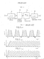
- a typical digital low-pass filter circuit for an audio circuit for example, an analog low-pass filter 41, a sample-holding circuit 42 and an A/D converter 43 are provided in a front stage, whereas a digital low-pass filter 40 is provided in a rear stage, as shown in FIG. 4.
- the analog low-pass filter 41 provided in front of the sample-holding circuit 42 removes a signal component whose frequency is higher than half of the sampling frequency so as to prevent aliasing.
- signal pass bands generally arise recurrently around the integer multiples of sampling frequency fs as shown in FIG. 5(A).
- the axis of the abscissa and the axis of the ordinate indicate the frequency f and the attenuated quantity L, respectively. Due to this characteristic, a desired low-pass filtering property generally cannot be achieved using only the digital low-pass filter 40.
- a low-pass filtering property as shown in FIG. 5(B) may be superposed with the analog low-pass filter 41 and provided in front of the sample-holding circuit 42 to prevent aliasing. As a result, the desired low-pass filtering property shown in FIG. 5(C) is achieved.
- the desired low-pass filtering property is thus achieved through the inclusion of the analog low-pass filter 41 in front of the sample-holding circuit 42 for the prevention of aliasing.
- a signal to be filtered by the circuit of FIG. 4 is an intermittent signal supplied from a rotary encoder or the like, there is no opportunity to transmit the signal through the analog low-pass filter 41 because the signal corresponds to an already sampled pseudo-digital signal. Consequently, the signal pass bands recurrently arise around higher frequencies as shown in FIG. 5(A) so that the desired low-pass filtering property cannot be achieved for the intermittent signal.
- a digital filter circuit which includes a plurality of digital filters which operate at mutually different clock frequencies and which are cascaded to each other.
- the clock frequencies are set so that the least common multiple thereof is equal to a high frequency at and above which the high-frequency component of a signal to be filtered by the digital filter circuit barely exists.
- the total frequency property of the cascaded digital filters is such that a second pass band of the frequency next higher than that of a first pass band for the DC component and so forth arises around the least common multiple of the clock frequencies.
- the relationship between the clock frequencies is adjusted to raise the second pass band to the high frequency at the end of the pass band at which the high-frequency component of the signal barely exists so that the desired low-pass filtering property is thus achieved.
- FIG. 1 shows a block diagram of the constitution of a digital low-pass filter circuit of an embodiment of the present invention.
- the circuit comprises a first digital low-pass filter 11 and a second digital low-pass filter 12 which are cascaded to each other between an input terminal I and an output terminal O.
- the first and the second digital low-pass filters 11 and 12 operate at different first and second clock frequencies fc1 and fc2, respectively.
- the first digital low-pass filter 11 comprises a buffer memory 21, one-clock-pulse delay circuits 22, 23, 24, 25 and 26, adders 27, 28, 29, 30 and 31, and coefficient means 32, 33 and 34, as shown by a block diagram in FIG. 2.
- the second digital low-pass filter 12 has the same constitution as the first digital low-pass filter 11 shown in FIG. 2 except that the second clock frequency fc2 is used instead of the first clock frequency fc1 for reading out the signal from the buffer memory and that the number of delay circuits and the coefficients of the coefficient means are different.
- the digital signal retained in the buffer memory 21 is then repeatedly read out at the first clock frequency fc1 so that the low-frequency component of the signal may be taken out through a digital low-pass filter section comprising the five cascaded one-clock-pulse delay circuits 22, 23, 24, 25 and 26, the adders 27, 28 and 29 for adding the delayed signals to each other, the coefficient means 32, 33 and 34 for multiplying the addition outputs of the adders by predetermined coefficients, and adders 30 and 31 for adding the outputs of the coefficient means to each other.
- the output of this digital low-pass filter section is then sent out from adder 31 via an output terminal O1.
- the filtering property of the first digital low-pass filter 11 is such that frequency pass bands recurrently arise around the integer multiples of the first clock frequency fc1, as shown in FIG. 3(A).
- the axis of the abscissa and the axis of the ordinate indicate the frequency f and the attenuated quantity L, respectively.
- the clock frequency fc2 for the second digital low-pass filter 12 may be set to be equal to one and a half times the clock frequency fc1 for the first digital low-pass filter 11.
- the filtering property of the second digital low-pass filter 12 is such that frequency pass bands recurrently arise around the integer multiples of the second clock frequency fc2, as shown in FIG. 3(B).
- the total filtering property of the digital low-pass filter circuit shown in FIG. 1 and comprising the first and the second digital low-pass filters 11 and 12 cascaded to each other consists of the superposition of the filtering properties of both the digital low-pass filters 11 and 12, as shown in FIG. 3(C).
- the relationship between the first and the second clock frequencies fc1 and fc2 can be adjusted in order to raise the second frequency pass band to a high frequency at and above which the high-frequency component of the signal to be filtered by the digital low-pass filter circuit barely exists.
- the total filtering property can be approximated to that of a desired low-pass filtering property by raising the second frequency pass band by a necessary quantity to the desired cutoff frequency for the pass band.
- the first and the second clock frequencies fc1 and fc2 are set at 1 kHz and 1.3 kHz, respectively.
- the second frequency pass band would then be raised to a high frequency of 13 kHz.
- the total filtering property can be approximated by setting the desired low-pass filtering cutoff (frequency multiple) by selecting the different clock frequencies to be of the necessary frequencies.
- the above-described embodiment is a digital low-pass filter circuit
- the present invention is not confined thereto, for it may be embodied as a digital band pass filter circuit, a band stop filter circuit or the like.
- every high-pass filter circuit does not have an infinitely high frequency pass band in reality, the circuit of the present invention substantially has a band pass filtering property. Consequently, the present invention can also be embodied as a high-pass filter circuit which substantially has a band pass filtering property.
Landscapes
- Physics & Mathematics (AREA)
- Engineering & Computer Science (AREA)
- Computer Hardware Design (AREA)
- Mathematical Physics (AREA)
- Analogue/Digital Conversion (AREA)
- Synchronisation In Digital Transmission Systems (AREA)
- Filters And Equalizers (AREA)
Applications Claiming Priority (2)
| Application Number | Priority Date | Filing Date | Title |
|---|---|---|---|
| JP30958786A JPH0744425B2 (ja) | 1986-12-29 | 1986-12-29 | デイジタル濾波回路 |
| JP309587/86 | 1986-12-29 |
Publications (2)
| Publication Number | Publication Date |
|---|---|
| EP0273100A2 true EP0273100A2 (de) | 1988-07-06 |
| EP0273100A3 EP0273100A3 (de) | 1989-11-23 |
Family
ID=17994828
Family Applications (1)
| Application Number | Title | Priority Date | Filing Date |
|---|---|---|---|
| EP87110771A Withdrawn EP0273100A3 (de) | 1986-12-29 | 1987-07-24 | Digitale Filterschaltung |
Country Status (2)
| Country | Link |
|---|---|
| EP (1) | EP0273100A3 (de) |
| JP (1) | JPH0744425B2 (de) |
Cited By (3)
| Publication number | Priority date | Publication date | Assignee | Title |
|---|---|---|---|---|
| US5111417A (en) * | 1988-08-30 | 1992-05-05 | International Business Machines Corp. | Digital filter sampling rate conversion method and device |
| GB2249680A (en) * | 1990-10-30 | 1992-05-13 | Secr Defence | Digital filters |
| US5867695A (en) * | 1992-10-16 | 1999-02-02 | International Business Machines Corp. | Method and system for reduced metastability between devices which communicate and operate at different clock frequencies |
Family Cites Families (2)
| Publication number | Priority date | Publication date | Assignee | Title |
|---|---|---|---|---|
| FR2273419B1 (de) * | 1973-01-25 | 1976-09-10 | Trt Telecom Radio Electr | |
| US3979701A (en) * | 1975-06-17 | 1976-09-07 | Communications Satellite Corporation (Comsat) | Non-recursive digital filter employing simple coefficients |
-
1986
- 1986-12-29 JP JP30958786A patent/JPH0744425B2/ja not_active Expired - Lifetime
-
1987
- 1987-07-24 EP EP87110771A patent/EP0273100A3/de not_active Withdrawn
Cited By (4)
| Publication number | Priority date | Publication date | Assignee | Title |
|---|---|---|---|---|
| US5111417A (en) * | 1988-08-30 | 1992-05-05 | International Business Machines Corp. | Digital filter sampling rate conversion method and device |
| GB2249680A (en) * | 1990-10-30 | 1992-05-13 | Secr Defence | Digital filters |
| GB2249680B (en) * | 1990-10-30 | 1994-09-07 | Secr Defence | Filters for digital information |
| US5867695A (en) * | 1992-10-16 | 1999-02-02 | International Business Machines Corp. | Method and system for reduced metastability between devices which communicate and operate at different clock frequencies |
Also Published As
| Publication number | Publication date |
|---|---|
| EP0273100A3 (de) | 1989-11-23 |
| JPS63167516A (ja) | 1988-07-11 |
| JPH0744425B2 (ja) | 1995-05-15 |
Similar Documents
| Publication | Publication Date | Title |
|---|---|---|
| US5398029A (en) | Sampling rate converter | |
| JPH0783233B2 (ja) | サンプリングされたデータ用バンド・パスろ波方法 | |
| EP1611679B1 (de) | Auf- und abwärtsabtastratenwandler | |
| AU9097391A (en) | A method to reduce the power consumation of a digital filter bank by reducing the number of multiplications | |
| WO1994023492A1 (en) | Decimation filter | |
| KR20040027371A (ko) | 데시메이션 필터 및 인터폴레이션 필터 | |
| EP0273100A2 (de) | Digitale Filterschaltung | |
| Lim et al. | Analysis and optimum design of the FFB | |
| JP4265119B2 (ja) | デジタルフィルタ | |
| US20030052804A1 (en) | Method for converting a plurality of signals from one of a digital and analogue form to the other form | |
| US5296822A (en) | Low pass filter circuit device and method having selectable cutoff frequency | |
| EP0565358A1 (de) | Linearer Phasenfilter mit umgekehrter Zeitbasis | |
| US5550764A (en) | Image filtering with an efficient implementation of high order decimation digital filters | |
| US6507300B1 (en) | Variable rate decimator | |
| WO1992009147A1 (en) | A method and arrangement for use in the elimination of echoes in a subscriber line circuit | |
| JPH1051269A (ja) | ローパスフィルタ | |
| Hamalainen | Optimization of multirate crossover filters | |
| Johansson | Multirate single-stage and multistage structures for high-speed recursive digital filtering | |
| JPS6229219A (ja) | アナログ信号の標本化回路 | |
| JPH01177708A (ja) | プログラマブルアナログフィルタ | |
| JPH0744426B2 (ja) | デイジタル濾波回路 | |
| JP3236440B2 (ja) | フィルタ回路装置 | |
| JPH057129A (ja) | デイジタル信号等化器 | |
| JPH08172338A (ja) | 半導体集積回路 | |
| JPH02172311A (ja) | 帯域通過フィルタ装置 |
Legal Events
| Date | Code | Title | Description |
|---|---|---|---|
| PUAI | Public reference made under article 153(3) epc to a published international application that has entered the european phase |
Free format text: ORIGINAL CODE: 0009012 |
|
| AK | Designated contracting states |
Kind code of ref document: A2 Designated state(s): DE FR GB |
|
| PUAL | Search report despatched |
Free format text: ORIGINAL CODE: 0009013 |
|
| RHK1 | Main classification (correction) |
Ipc: H03H 17/02 |
|
| AK | Designated contracting states |
Kind code of ref document: A3 Designated state(s): DE FR GB |
|
| 17P | Request for examination filed |
Effective date: 19900523 |
|
| 17Q | First examination report despatched |
Effective date: 19910227 |
|
| STAA | Information on the status of an ep patent application or granted ep patent |
Free format text: STATUS: THE APPLICATION IS DEEMED TO BE WITHDRAWN |
|
| 18D | Application deemed to be withdrawn |
Effective date: 19910910 |
|
| RIN1 | Information on inventor provided before grant (corrected) |
Inventor name: KUMASAKA, TORUNEC HOME ELECTRONICS LTD. |